Archive for the ‘Ponderings’ Category

What’s the Value of Hackable Hardware, Anyway?

Friday, December 11th, 2020

There is plenty of skepticism around the value of hackable products. Significantly, hackability is different from openness: cars are closed-source, yet support vibrant modding communities; gcc is one of the “real OG”s of open source, but few users find it easy to extend or enhance. Is it better to have a garden planted by the most knowledgeable botanists and maintained by experienced gardeners, or an open plot of land maintained by whoever has the interest and time?


Above left: Walled garden of Edzell Castle; above right: Thorncliffe Park community garden.

In the case of hardware products, consumer behavior consistently affirms a strong preference for well-curated gardens. Hardware is hard – not only is it difficult to design and validate, supply chains benefit from economies of scale and predictable user demand. The larger a captive audience, the more up-front money one can invest into developing a better hardware product. However, every decision to optimize comes with inherent trade-offs. For example, anytime symmetry is broken, one must optimize for either a right-handed or a left-handed version.


Above: touching the spot indicated by the red arrow would degrade antenna performance on an iPhone 4. This spot would naturally rest on the palm of a left-handed user. Image adapted from “iPhone 4” by marc.flores, licensed under CC BY 2.0.

Some may recall a decade ago when the iPhone 4 was launched, left-handed people noticed the phone would frequently drop calls. It turned out the iPhone 4 was designed with a critical antenna element that would fail when held naturally by a left-handed person. The late Steve Jobs responded to this problem by telling users to “just avoid holding it that way”. Even if he didn’t mean it, I couldn’t help but feel like he was saying the iPhone 4 was perfect and left-handers like me were just defective humans who should be sent to re-education camps on how to hold things.

Of course, as a hardware engineer, I can also sympathize with why Steve Jobs might have felt this way – clearly, a huge amount of effort and thought went into designing a technical masterpiece that was also of museum-quality construction. It’s frustrating to be told, after spending years and billions of dollars trying to build “the perfect product” that they somehow got it wrong because humans aren’t a homogeneous population. Rumors have it Apple spent tens of millions of dollars building micron-precision production jigs out of injection-molding grade tooling to ensure the iPhone4 was simply perfect in terms of production tolerances; duplicating all of those to make a mirror-image version for left-handers that make up 10% of the market size just made no business sense. It proved to be cheaper and easier, ultimately, to take full refunds or to give out rubber bumpers to the users who requested them.

I do think there is such a thing as “over-designing” a product. For example, contemporary “high concept” smartphone design is minimalist – phone companies have removed headphone jacks, hidden the front camera, and removed physical buttons. There is clearly no place for screws in this world; the love affair of smartphones and adhesives has proven to be … sticky. Adhesives, used in place of screws in modern smartphones, are so aggressive that removing them either requires additional equipment, such as a hot plate and solvents, or simply destroying the outer bezel by breaking the outer case off in pieces and replacing it with an entirely new bezel upon re-assembly. In other words, hacking a modern smartphone necessarily implies the destruction or damage of adhesive-bound parts.

With Precursor, I’m bringing screws back.

Precursor’s screws are unapologetic – I make no attempt to hide them or cover them with bits of tape or rubber inserts. Instead, I’ve sourced custom-made Torx T3 metric screws with a black oxide finish that compliments the overall color scheme of Precursor. Six of them line the front, as a direct invitation for users to remove them and see what’s inside. I’ve already received ample criticism for the decision to show screws as “primitive”, “ugly”, “out of touch with modern trends” — but in the end, I feel the visual clutter of these six screws is a small price to pay for the gain in hackability.

Of course, the anti-screw critics question the value of hackability. Surely, I am sacrificing mass-market appeal to enable a fringe market; if hackability was so important, wouldn’t Apple and Google already have incorporated it into their phones? Wouldn’t we see more good examples of hackability already?

This line of questioning is circular: you can’t get good examples of hacks until you have made hackable products wide-spread. However, the critics are correct, in a way: in order to bootstrap an ecosystem, we’re going to need some good examples of why hackability matters.

In the run-up to crowdfunding Precursor, I was contemplating a good demo hack for Precursor. Fortuitously, a fellow named Matt Campbell opened a GitHub issue requesting a text-to-speech option for blind users. This led me to ask what might be helpful in terms of a physical keyboard design to assist blind people. You can read the thread for yourself, but I’ll highlight that even the blind community itself is divided on whether or not there is such a thing as the “blind ghetto” — an epithet applied by some users who feel that blindness-specific products tend to lag behind modern smartphones, tablets, and laptops. However, given that most modern gadgets struggle to consider the needs of 10% of the population that’s left-handed, I’m readily sympathetic to the notion that gadgets make little to no concession to accommodate the even smaller number of blind users.

Matt was articulate in specifying his preferred design for a pocketable keyboard. He referred me to the “Braille ‘n Speak” (shown above) as an example of an existing braille keyboard. Basically, it takes the six dots that make up braille, and lines them up horizontally into three left and three right sets of buttons, adding a single button in the middle that functions as a space bar. Characters are entered by typing chords that correspond to the patterns of the six dots in the braille alphabet. Not being a braille user myself, I had to look up what the alphabet looked like. I made the guide below based on a snippet from Wikipedia to better understand how such a keyboard might be used.

Ironically, even though Matt had linked me to the picture of the Braille n’ Speak, it still took a while to sink in that a braille variant of Precursor did not need a display. I’m a bit ashamed to admit my first sketches involved trying to cram this set of switches into the existing keyboard area of the Precursor, without first removing the display entirely. I had to overcome my own prejudice about how the world should look and it took me time and empathy to understand this new perspective.

Once I had a better grasp of Matt’s request, I set about designing a customized braille variant. Precursor was designed for this style of hacking: the keyboard is a simple 2-layer PCB that’s cheap and easy to re-design, and the front bezel is also a PCB, which is a bit more expensive to redesign. Fortunately, I was able to amortize setup costs by bundling the braille front bezel variant with another variant that I had to fabricate anyways for the crowdfunding campaign. Beyond that, I also had to come up with some custom key caps to complement the switches.

The major challenge in designing any type of mobile-friendly keyboard is always a trade-off between the hand feel of the switches, versus thinness of the overall design. On one side of the spectrum, full-travel mechanical switches have a wonderful hand feel, but are thicker than a sausage. On the other side of the spectrum, dome switches and printed carbon ink patterns are thinner than a credit card, but can feel mushy and have a limited “sweet spot” — the region of a key switch with optimal tactile feedback and operational force curves. The generally well-regarded Thinkpad keyboards go with a middle-ground solution that’s a few millimeters thick, using a “scissor” mechanism to stabilize the key caps over a silicone dome switch, giving individual keys a bit of travel while ensuring that the “sweet spot” covers the entire key cap. Optimizing key switch mechanisms is hard: some may recall the controversy over Apple’s re-design of the MacBook’s keyboard to use a “butterfly” mechanism, which shaved a couple mm of thickness, but led to lawsuits over a defect where the keyboard allegedly stopped working when small bits of dust or other particles got trapped under it.

Given the short time frame and a shoestring budget, I decided to use an ultra-thin (0.35mm) tactile switch that I could buy off-the-shelf from Digikey and create custom key caps with small dimples to assist users in finding the relatively small sweet spots typical of such switches. I have sincere hopes this is a pretty good final solution; while it lacks a scissor mechanism to spread off-centered force, the simple mechanism meant I didn’t have to stick with a square key cap and could do something more comfortable and ergonomic to focus forces into the sweet spot. At the very least, the mechanism would be no worse than the current mechanism used in Precursor’s existing keyboard for sighted users, which is similarly a dome switch plus a hybrid-polymer key film.

Next, I had to figure out where to place the switches. To assist with this, I printed a 1:1 scale version of the Precursor case, dipped my fingertips in ink, and proceeded to tap on the printout in what felt like a natural fashion.

I then took the resulting ink spots and dimensioned their centers, to place the centroid of each key cap. I also asked my partner, who has smaller hands, to place her fingers over the spots and noted the differences in where her fingers lay to help shape the final key caps for different-sized hands.

Next, using the “master profile” discussed in the previous post on Precursor’s mechanical design, I translated this into a sketch to help create a set of key caps based on splines that matched the natural angle of fingers.

Above, you can see an early sketch of the key caps, showing the initial shape with dimples for centering the fingers.

Before moving ahead and spending a few hundred dollars to build a functional prototype, I decided to get Matt’s feedback on the design. We submitted the design to Shapeways and had a 3D print sent to Matt, which he graciously paid for. After receiving the plastic dummy, his feedback was that the center space bar should be a single key, instead of two separate keys, so I merged the two separate key caps of the space bar together into a single piece, while retaining two separate switches wired in parallel under the space bar. I felt this was a reasonable compromise that would allow for a “sweet spot” that serviced lefties as well as righties.

I then re-designed the keyboard PCB, which was a fairly simple task, because the braille keyboard consists of only eight switches. I just had to be careful to pick row/column pairs that would not conflict during chording and be sure to include the row/column pairs necessary to turn Precursor on after being put to sleep. I also redesigned the bezel; eliminating the display actually makes manufacturing a little bit easier because it also removes a beveling step in the manufacturing process. I kept the RF antenna in exactly the same location, as its design was already well-characterized and it takes a lot of effort to tune the antenna. Finally, I decided to manufacture the key switches out of aluminum. The switches have a lot of fine features and I needed a stiff material that could translate off-target force to the key switches to enlarge the sweet spot as much as possible.


Above: The prototype of Precursor with braille keyboard.

About three weeks later, all the parts for the braille keyboard had arrived. I decided to use purple anodization for the key switches which, combined with the organic key shapes, gives the final design a bit of a Wakanda-esque “Black Panther” aesthetic, especially when mounted in a brass case. The key switch feel is about in line with what I imagined, with the caveat that one of the switches feels a little less nice than the rest, but I think that’s due to a bad solder job on the switch itself. I haven’t had a chance to trace it down because…well, I’ve had to write a bunch of posts like this to fund Precursor. I have also been working with Xobs to refactor Xous in hopes of putting together enough code to send Matt a prototype he can evaluate without having to write gobs of embedded hardware driver code himself.

Above is a quick photo showing the alignment of fingers to keys. Naturally, it’s perfect for my hand because it was designed around it. I’m looking forward to hearing Matt’s opinion about the feel of the keys.

Above is a photo of the custom parts for the braille keyboard. At the top, you can see the custom bezel with key caps and the RF antenna matching circuitry on the top right. On the bottom, you can see the custom keyboard PCB mounted onto a Precursor motherboard. The keyboard PCB is mostly blank and, because of the small number of keys and the flexibility of the FPGA, there’s an option to mount more peripherals on the PCB.

Despite not being yet finalized, I hope this exercise is sufficient to demonstrate the potential value of hackable products. The original design scope for Precursor (née Betrusted) did not explicitly include a braille keyboard option, but thanks to modular design principles and the use of accessible construction materials, I was able to produce a prototype in about a month that has a similar fit and finish as the mainstream product.

As long as humans choose to embrace diversity, I think hackability will have value. A notional “perfect” product implies there’s such a thing as a “perfect” user. However, in reality, even the simple conundrum of left- or right-handedness challenges the existence of a singular “perfect” product for all of humanity. Fortunately, accommodating the wonderfully diverse, quirky, and interesting range of humanity implicates just a few simple engineering principles, such as embracing screws over adhesives, openness, and modularity. That we can’t hack our products isn’t a limitation of physics and engineering. Precursor demonstrates one can build something simultaneously secure and hackable, while being compact and pocketable. This suggests the relative lack of hackable products on the market isn’t a fundamental limitation. Maybe we just need a little more imagination, maybe we need to be a little more open-minded about aesthetics, and maybe companies need to be willing to take brave steps toward openness and inclusivity.

For Apple, true “courage to move on and do something new that betters all of us” was to remove the headphone jack, which resulted in locking users deeper into a walled-garden ecosystem. For hackers like myself, our “courage” is facing blunt criticisms for making “ugly” products with screws in order to facilitate mods, such as braille keyboards, in order to expand the definition of “all of us” beyond a set of privileged, “perfect” users.

I hope this braille keyboard is just the first example of many mods for Precursor that adapt the product for unique end-users, bucking the trend of gaslighting users to mold their behavior and preferences to fit the product. If you’ve got an itch to develop your own yet-to-be-seen feature in a mobile device, please visit our crowdfunding campaign page to learn more about Precursor. We’re close to being funded, but we’ve only a few days left in the campaign. After the campaign concludes on December 15th, the limited edition will no longer be available, and pricing of the standard model goes up. If you like what you see, please consider helping us to bring Precursor to life!

On Liberating My Smartwatch From Cloud Services

Saturday, July 25th, 2020

I’ve often said that if we convince ourselves that technology is magic, we risk becoming hostages to it. Just recently, I had a brush with this fate, but happily, I was saved by open source.

At the time of writing, Garmin is suffering from a massive ransomware attack. I also happen to be a user of the Garmin Instinct watch. I’m very happy with it, and in many ways, it’s magical how much capability is packed into such a tiny package.

I also happen to have a hobby of paddling the outrigger canoe:

I consider the GPS watch to be an indispensable piece of safety gear, especially for the boat’s steer, because it’s hard to judge your water speed when you’re more than a few hundred meters from land. If you get stuck in a bad current, without situational awareness you could end up swept out to sea or worse.

The water currents around Singapore can be extreme. When the tides change, the South China Sea eventually finds its way to the Andaman Sea through the Singapore Strait, causing treacherous flows of current that shift over time. Thus, after every paddle, I upload my GPS data to the Garmin Connect cloud and review the route, in part to note dangerous changes in the ebb-and-flow patterns of currents.

While it’s a clear and present privacy risk to upload such data to the Garmin cloud, we’re all familiar with the trade-off: there’s only 24 hours in the day to worry about things, and the service just worked so well.

Until yesterday.

We had just wrapped up a paddle with particularly unusual currents, and my paddling partner wanted to know our speeds at a few of the tricky spots. I went to retrieve the data and…well, I found out that Garmin was under attack.

Garmin was being held hostage, and transitively, so was access to my paddling data: a small facet of my life had become a hostage to technology.

A bunch of my paddling friends recommended I try Strava. The good news is Garmin allows data files to be retrieved off of the Instinct watch, for upload to third-party services. All you have to do is plug the watch into a regular USB port, and it shows up as a mass storage device.

The bad news is as I tried to create an account on Strava, all sorts of warning bells went off. The website is full of dark patterns, and when I clicked to deny Strava access to my health-related data, I was met with this tricky series dialog boxes:

Click “Decline”…

Click “Deny Permission”…

Click “OK”…

Three clicks to opt out, and if I wasn’t paying attention and just kept clicking the bottom box, I would have opted-in by accident. After this, I was greeted by a creepy list of people to follow (how do they know so much about me from just an email?), and then there’s a tricky dialog box that, if answered incorrectly, routes you to a spot to enter credit card information as part of your “free trial”.

Since Garmin at least made money by selling me a $200+ piece of hardware, collecting my health data is just icing on the cake; for Strava, my health data is the cake. It’s pretty clear to me that Strava made a pitch to its investors that they’ll make fat returns by monetizing my private data, including my health information.

This is a hard no for me. Instead of liberating myself from a hostage situation, going from Garmin to Strava would be like stepping out of the frying pan and directly into the fire.

So, even though this was a busy afternoon … I’m scheduled to paddle again the day after tomorrow, and it would be great to have my boat speed analytics before then. Plus, I was sufficiently miffed by the Strava experience that I couldn’t help but start searching around to see if I couldn’t cobble together my own privacy-protecting alternative.

I was very pleased to discovered an open-source utility called gpsbabel (thank you gpsbabel! I donated!) that can unpack Garmin’s semi-(?)proprietary “.FIT” file format into the interoperable “.GPX” format. From there, I was able to cobble together bits and pieces of XML parsing code and merge it with OpenStreetMaps via the Folium API to create custom maps of my data.

Even with getting “lost” on a detour of trying to use the Google Maps API that left an awful “for development only” watermark on all my map tiles, this only took an evening — it wasn’t the best possible use of my time all things considered, but it was mostly a matter of finding the right open-source pieces and gluing them together with Python (fwiw, Python is a great glue, but a terrible structural material. Do not build skyscrapers out of Python). The code quality is pretty crap, but Python allows that, and it gets the job done. Given those caveats, one could use it as a starting point for something better.

Now that I have full control over my data, I’m able to visualize it in ways that make sense to me. For example, I’ve plotted my speed as a heat map map over the course, with circles proportional to the speed at that moment, and a hover-text that shows my instantaneous speed and heart rate:

It’s exactly the data I need, in the format that I want; no more, and no less. Plus, the output is a single html file that I can share directly with nothing more than a simple link. No analytics, no cookies. Just the data I’ve chosen to share with you.

Here’s a snippet of the code that I use to plot the map data:

Like I said, not the best quality code, but it works, and it was quick to write.

Even better yet, I’m no longer uploading my position or fitness data to the cloud — there is a certain intangible satisfaction in “going dark” for yet another surveillance leakage point in my life, without any compromise in quality or convenience.

It’s also an interesting meta-story about how healthy and vibrant the open-source ecosystem is today. When the Garmin cloud fell, I was able to replace the most important functions of it in just an afternoon by cutting and pasting together various open source frameworks.

The point of open source is not to ritualistically compile our stuff from source. It’s the awareness that technology is not magic: that there is a trail of breadcrumbs any of us could follow to liberate our digital lives in case of a potential hostage situation. Should we so desire, open source empowers us to create and run our own essential tools and services.

Edits: added details on how to take data off the watch, and noted the watch’s price.

On Contact Tracing and Hardware Tokens

Monday, June 22nd, 2020

Early in the COVID-19 pandemic, I was tapped by the European Commission to develop a privacy-protecting contact tracing token, which you can read more about at the Simmel project home page. And very recently, Singapore has announced the deployment of a TraceTogether token. As part of their launch, I was invited to participate in a review of their solution. The urgency of COVID-19 and the essential challenges of building supply chains means we are now in the position of bolting wheels on a plane as it rolls down the runway. As with many issues involving privacy and technology, this is a complicated and nuanced situation that cannot be easily digested into a series of tweets. Thus, over the coming weeks I hope to offer you my insights in the form of short essays, which I will post here.

Since I was only able to spend an hour with the TraceTogether token so far, I’ll spend most of this essay setting up the background I’ll be using to evaluate the token.

Contact Tracing

The basic idea behind contact tracing is simple: if you get sick, identify your close contacts, and test them to see if they are also sick. If you do this fast enough, you can contain COVID-19, and most of society continues to function as normal.

However, from an implementation standpoint, there are some subtleties that I struggled to wrap my head around. Dr. Vivian Balakrishnan, the Minister-in-charge of the Smart Nation Initiative, briefly stated at our meeting on Friday that the Apple/Google Exposure Notification system did not reveal the “graph”. In order to help myself understand the epidemiological significance of extracting the contact graph, I drew some diagrams to illustrate contact tracing scenarios.

Let’s start by looking at a very simple contact tracing scenario.

In the diagram above, two individuals are shown, Person 1 and Person 2. We start Day 1 with Person 1 already infectious yet only mildly symptomatic. Person 1 comes in contact with Person 2 around mid-day. Person 2 then incubates the virus for a day, and becomes infectious late on Day 2. Person 2 may not have any symptoms at this time. At some future date, Person 2 infects two more people. In this simple example, it is easy to see that if we can isolate Person 2 early enough, we could prevent at least two future exposures to the virus.

Now let’s take a look at a more complicated COVID-19 spread scenario with no contact tracing. Let’s continue to assume Person 1 is a carrier with mild to no symptoms but is infectious: a so-called “super spreader”.

The above graphic depicts the timelines of 8 people over a span of five days with no contact tracing. Person 1 is ultimately responsible for the infection of several people over a period of a few days. Observe that the incubation periods are not identical for every individual; it will take a different amount of time for every person to incubate the virus and become infectious. Furthermore, the onset of symptoms is not strongly correlated with infectiousness.

Now let’s add contact tracing to this graph.

The graphic above illustrates the same scenario as before, but with the “platonic ideal” of contact tracing and isolation. In this case, Person 4 shows symptoms, seeks testing, and is confirmed positive early on Day 4; their contacts are isolated, and dozens of colleagues and friends are spared from future infection. Significantly, digging through the graph of contacts also allows one to discover a shared contact of Person 4 and Person 2, thus revealing that Person 1 is the originating asymptomatic carrier.

There is a subtle distinction between “contact tracing” and “contact notification”. Apple/Google’s “Exposure Notification” system only perform notifications to the immediate contacts of an infected person. The significance of this subtlety is hinted by the fact that the protocol was originally named a “Privacy Preserving Contact Tracing Protocol”, but renamed to the more accurate description of “Exposure Notification” in late April.

To better understand the limitations of exposure notification, let’s consider the same scenario as above, but instead of tracing out the entire graph, we only notify the immediate contacts of the first person to show definite symptoms – that is, Person 4.

With exposure notification, carriers with mild to no symptoms such as Person 1 would get misleading notifications that they were in contact with a person who tested positive for COVID-19, when in fact, it was actually the case that Person 1 gave COVID-19 to Person 4. In this case, Person 1 – who feels fine but is actually infectious – will continue about their daily life, except for the curiosity that everyone around them seems to be testing positive for COVID-19. As a result, some continued infections are unavoidable. Furthermore, Person 2 is a hidden node from Person 4, as Person 2 is not within Person 4’s set of immediate notification contacts.

In a nutshell, Exposure Notification alone cannot determine causality of an infection. A full contact “graph”, on the other hand, can discover carriers with mild to no symptoms. Furthermore, it has been well-established that a significant fraction of COVID-19 infections show mild or no symptoms for extended periods of time – these are not “rare” events. These individuals are infectious but are well enough to walk briskly through crowded metro stations and eat at hawker stalls. Thus, in the “local context” of Singapore, asymptomatic carriers can seed dozens of clusters in a matter of days if not hours, unlike less dense countries like the US, where infectious individuals may come in contact with only a handful of people on any given day.

The inability to quickly identify and isolate mildly symptomatic super-spreaders motivates the development of the local TraceTogether solution, which unlocks the potential for “full graph” contact tracing.

On Privacy and Contact Tracing

Of course, the privacy implications of full-graph contact tracing are profound. Also profound are the potential health risks and loss of life absent full-graph contact tracing. There’s also a proven solution for containing COVID-19 that involves no sacrifice of privacy: an extended Circuit-Breaker style lockdown. Of course, this comes at the price of the economy.

Of the three elements of privacy, health, or economy, it seems we can only pick two. There is a separate and important debate about which two we should prioritize, but that is beyond the context of this essay. For the purpose of this discussion, let’s assume contact tracing will be implemented. In this case, it is incumbent upon technologists like us to try and come up with a compromise that can mitigate the privacy impact while facilitating public policy.

Back in early April, Sean ‘xobs’ Cross and I were contacted by the European Commission’s NGI program via NLnet to propose a privacy-protecting contact tracing hardware token. The resulting proposal is called “Simmel”. While not perfect, the salient privacy features of Simmel include:

  1. Strong isolation of user data. By disallowing sensor fusion with the smartphone, there is zero risk of GPS or other geolocation data being leaked. It is also much harder to do metadata-based attacks against user privacy.
  2. Citizens are firmly in control. Users are the physical keeper of their contact data; no third-party servers are involved, until they volunteer their data to an authority by surrendering the physical token. This means in an extreme case, a user has the option of physically destroying their token to erase their history.
  3. Citizens can temporarily opt-out. By simply twisting the cap of the token, users can power the token down at any time, thus creating a gap in their trace data (note: this feature is not present on the first prototypes).
  4. Randomized broadcast data. This is a protocol-level feature which we recommend to defeat the ability for third parties (perhaps an advertising agency or a hostile government) from piggy backing on the protocol to aggregate user locations for commercial or strategic benefit.

Why a Hardware Token?

But why a hardware token? Isn’t an app just better in so many ways?

At our session on Friday, the TraceTogether token team stated that Singapore needs hardware tokens to better serve two groups: the underprivileged, and iPhone users. The underprivileged can’t afford to buy a smartphone; and iPhone users can only run Apple-approved protocols, such as their Exposure Notification service (which does not enable full contact tracing). In other words, iPhone users, like the underprivileged, also don’t own a smartphone; rather, they’ve bought a phone that can only be used for Apple-sanctioned activities.

Our Simmel proposal makes it clear that I’m a fan of a hardware token, but for reasons of privacy. It turns out that apps, and smartphones in general, are bad for user privacy. If you genuinely care about privacy, you would leave your smartphone at home. The table below helps to illustrate the point. A red X indicates a known plausible infraction of privacy for a given device scenario.

The tracing token (as proposed by Singapore) can reveal your location and identity to the government. Nominally, this happens at the point where you surrender your token to the health authorities. However, in theory, the government could deploy tens of thousands of TraceTogether receivers around the island to record the movement of your token in real-time. While this is problematic, it’s relevant to compare this against your smartphone, which typically broadcasts a range of unique, unencrypted IDs, ranging from the IMEI to the wifi MAC address. Because the smartphone’s identifiers are not anonymized by default, they are potentially usable by anyone – not just the government – to identify you and your approximate location. Thus, for better or for worse, the design of the TraceTogether token does not meaningfully change the status quo as far as “big infrastructure” attacks on individual privacy.

Significantly, the tracing token employs an anonymization scheme for the broadcast IDs, so it should not be able to reveal anything about your location or identity to third parties – only to the government. Contrast this to the SafeEntry ID card scanner, where you hand over your ID card to staff at SafeEntry kiosks. This is an arguably less secure solution, as the staff member has an opportunity to read your private details (which includes your home address) while scanning your ID card, hence the boxes are red under “location” and “identity”.

Going back to the smartphone, “typical apps” – say, Facebook, Pokemon Go, Grab, TikTok, Maps – are often installed with most permissions enabled. Such a phone actively and routinely discloses your location, media, phone calls, microphones, contacts, and NFC (used for contactless payment and content beaming) data to a wide variety of providers. Although each provider claims to “anonymize” your data, it has been well-established that so much data is being published that it is virtually a push of a button to de-anonymize that data. Furthermore, your data is subject to surveillance by several other governments, thanks to the broad power of governments around the world to lawfully extract data from local service providers. This is not to mention the ever-present risk of malicious actors, exploits, or deceptive UI techniques to convince, dupe, or coerce you to disclose your data.

Let’s say you’re quite paranoid, and you cleverly put your iPhone into airplane mode most of the time. Nothing to worry about, right? Wrong. For example, in airplane mode, the iPhone still runs its GPS receiver and NFC. An independent analysis I’ve made of the iPhone also reveals occasional, unexplained blips on the wifi interface.

To summarize, here are the core arguments for why a hardware token offers stronger privacy protections than an app:

No Sensor Fusion

The data revealed by a hardware token is strongly limited by its inability to perform “sensor fusion” with a smartphone-like sensor suite. And even though I was only able to spend an hour with the device, I can say with a high degree of confidence that the TraceTogether token has little to no capability beyond the requisite BLE radio. Why do I say this? Because physics and economics:

Physics: more radios and sensors would draw more power. Ever notice how your phone’s battery life is shorter if location services are on? If the token is to last several months on such a tiny battery, there simply is not enough power available to operate much more than the advertised BLE functions.
Economics: more electronics means more cost. The publicly disclosed tender offering places a cap on the value of parts at S$20, and it essentially has to be less than that because the producer must also bear their development cost out of the tender. There is little room for extraneous sensors or radios within that economic envelope.

Above: the battery used in the TraceTogether token. It has a capacity of 1000mAh. The battery in your smartphone has a capacity of around 3x of this, and requires daily charging.

The economics argument is weaker than the physics argument, because the government could always prepare a limited number of “special” tokens to track select individuals at an arbitrary cost. However, the physics argument still stands – no amount of money invested by the government can break the laws of physics. If Singapore could develop a mass-manufacturable battery that can power a smartphone sensor suite for months in that form factor – well, let’s just say the world would be a very different place.

Citizen Hegemony over Contact History

Assuming that the final TraceTogether token doesn’t provide a method to repurpose the Bluetooth Low-Energy (BLE) radio for data readout (and this is something we hope to confirm in a future hackathon), citizens have absolute hegemony over their contact history data, at least until they surrender it in a contact tracing event.

As a result the government is, perhaps inadvertently, empowering citizens to rebel against the TraceTogether system: one can always crush their token and “opt-out” of the system (but please remove the battery first, otherwise you may burn down your flat). Or perhaps more subtly, you can “forget your token at home”, or carry it in a metallized pouch to block its signal. The physical embodiment of the token also means that once the COVID-19 pandemic is under control, destroying the token definitively destroys the data within it – unlike an app, where too often uninstalling the app simply means an icon is removed from your screen, but some data is still retained as a file somewhere on the device.

In other words, a physical token means that an earnest conversation about privacy can continue in parallel with the collection of contact tracing data. So even if you are not sure about the benefit of TraceTogether today, carrying the token allows you to defer the final decision of whether to trust the government until the point where you are requested to surrender your token for contact trace extraction.

If the government gets caught scattering BLE receivers around the island, or an errant token is found containing suspicious circuitry, the government stands to lose not just the trust of the people, but also access to full-graph contact tracing as citizens and residents dispose of tokens en masse. This restores a certain balance of power, where the government can and will be held accountable to its social contract, even as we amass contact tracing data together as a whole.

Next Steps

When I was tapped to independently review the TraceTogether token, I told the government that I would hold no punches – and surprisingly, they still invited me to the introductory session last Friday.

This essay framed the context I will use to evaluate the token. “Exposure notification” is not sufficient to isolate mildly symptomatic carriers of COVID-19, whereas “full graph” contact tracing may be able to make some headway against this problem. The good news is that the introduction of a physically embodied hardware token presents a safer opportunity to continue the debate on privacy while simultaneously improving the collection of contact tracing data. Ultimately, deployment of a hardware token system relies upon the compliance of citizens, and thus it is up to our government to maintain or earn our trust to manage our nation’s best interests throughout this pandemic.

I look forward to future hackathons where we can really dig into what’s running inside the TraceTogether token. Until then, stay safe, stay home when you can, and when you must go outside, wear your mask!

PS: You should also check out Sean ‘xobs’ Cross’ teardown of the TraceTogether token!

Formlabs Form 3 Teardown

Tuesday, January 7th, 2020

It’s been my privilege to do teardowns on both the Formlabs Form 1 and Form 2. With the recent release of the Form 3, I was asked by Formlabs if I wanted to do another teardown, and of course I jumped on the opportunity. I always learn an immense amount while taking apart their machines, and it’s also been very satisfying to watch their engineering team grow and mature over the years.

Form 3 First Impressions

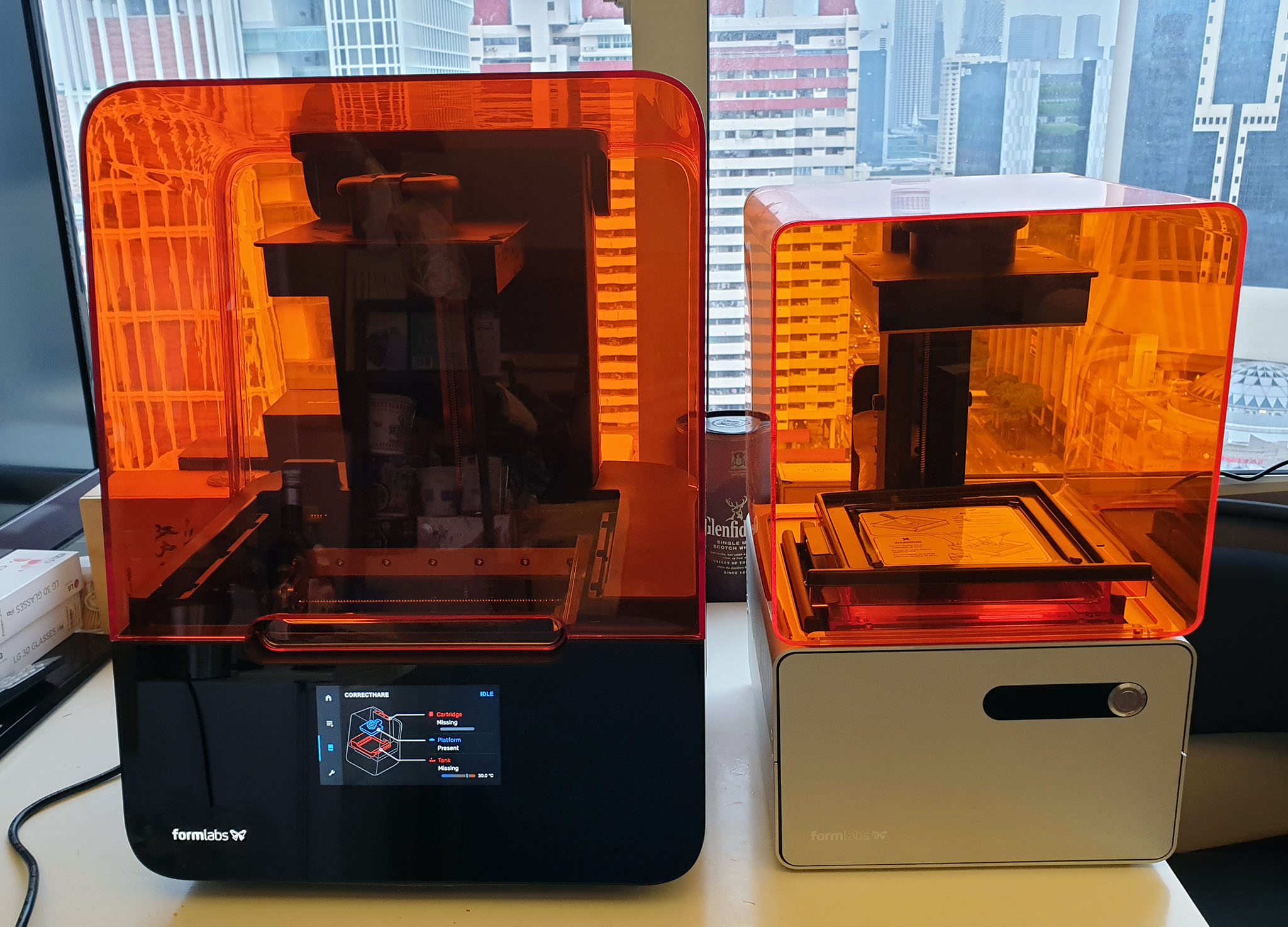
My first impression of the Form 3 was, “wow, this is a big machine”.

Above is a Form 3 next to a Form 1 for size comparison. The Form 3 build platform is a little larger than the Form 1, but it turns out there are a number of good reasons for the extra size, which we’ll get into later.

Before taking the whole machine apart, I decided I’d give it at least one test print. So, I went and downloaded a couple of popular-looking prints from the Internet and loaded them into the latest version of the Preform software. The design I had chosen was quite large, requiring over 18 hours to print in clear resin. This was not going to cut it for a quick test print! Fortunately, Formlabs had also sent me a sample of their “draft resin”, which advertises itself as a way to rough out quick, low-resolution prints. Indeed, migrating the design to the draft resin reduced the print time down to under 4 hours, which was a welcome relief for a quick test print.

The resin still yielded a part with reasonably crisp lines, although as expected the layers were quite visible. The main downside was that the part as printed was virtually impossible to remove from its support material. I suspect this might have been a user error, because I had changed the resin from clear to draft: I thought I had asked Preform to recompute the support material structure, but it seems that didn’t happen.

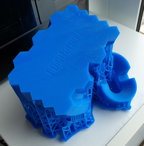
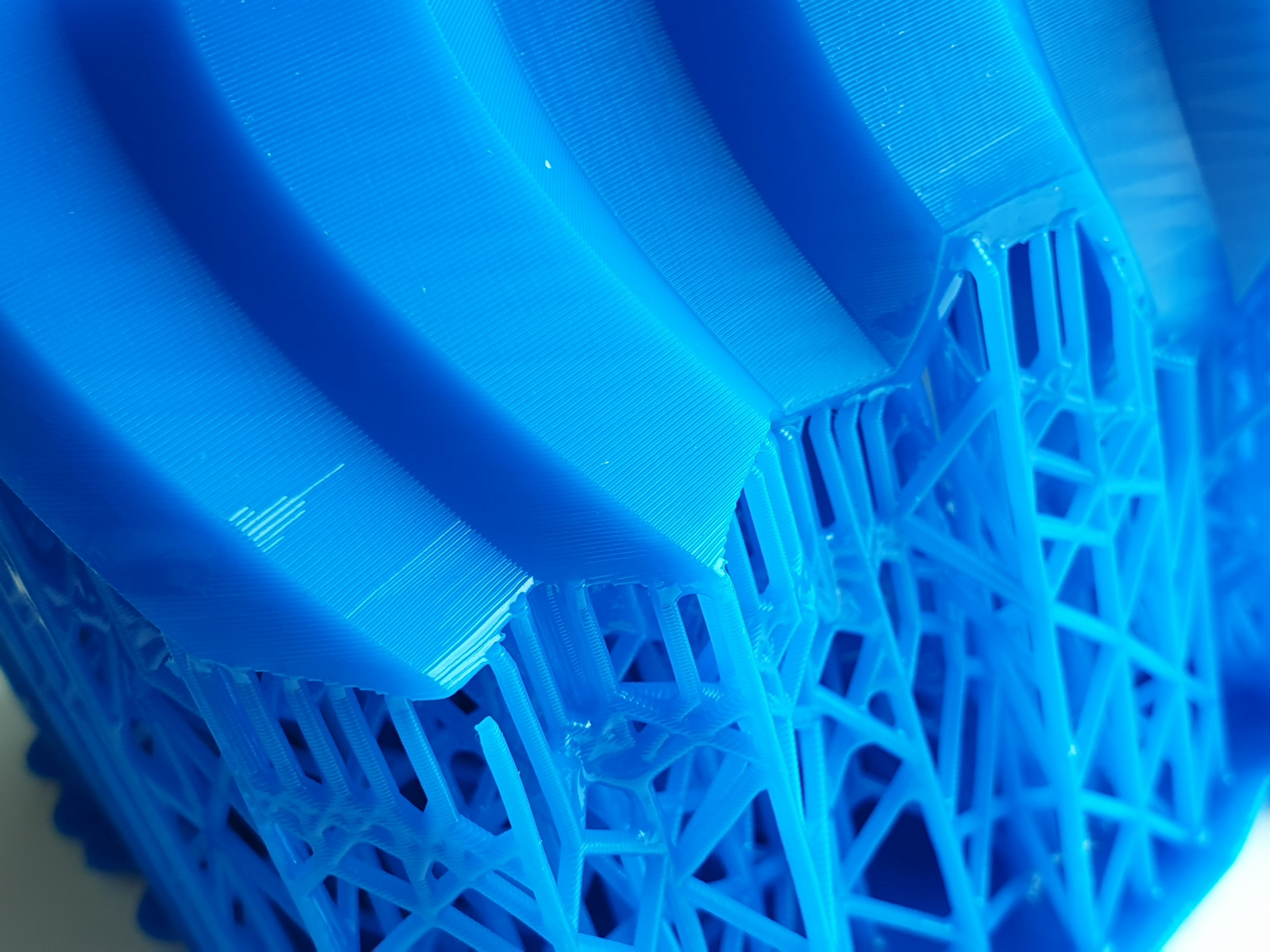
Above: a view of the test part, printed in draft resin.

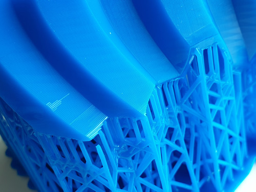
Above: close-up of the rather robust support material connection to the print.

Aside from woes trying to remove the part from the support material, the other issues I had with the draft resin is its strong smell, and its sensitivity to ambient light. Everyone in the office became quite aware that I was using the draft resin due to its strong odor, so once the print was finished I endeavored to bottle up as much of the resin as I could, thus limiting the nuisance odor to others in the office. However, as I was handling the resin, I could see the draft resin was quickly curing in the ambient light, so I had to work quickly and pour it back into the bottle as a thin crust of material formed. Its increased photosensitivity makes sense, given that it is tuned for fast printing and curing, but it does make it a bit trickier to handle.

Overall, I’d probably give the draft resin another try because the fast print times are appealing, but that’ll be for another day – on to the teardown!

Exterior Notes

Even without removing a single screw, there’s a couple of noteworthy observations to share about the Form 3’s construction. Let’s start with the front panel UI.

The Form 3 doubles down on the sleek, movie-set ready UI of the Form 2.

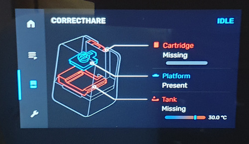
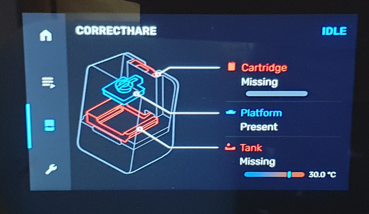
Above is an example screen from the Form 3’s integrated display. In addition to a graphical style that would be at home in Tony Stark’s lab, the image above shows off the enhanced introspection capabilities of the printer. The Form 3 is more aware of its accessories and environment than ever; for example, it now has the ability to report a missing build platform.

One problem that became immediately evident to me, however, was a lack of a way to put the Form 3 into standby. I searched through the UI for a soft-standby option, but couldn’t find it. Perhaps it’s there, but it’s just very well hidden. However, the lack of a “hard” button to turn the system on from standby is possibly indicative of a deliberate choice to eliminate standby as an option. For good print quality, it seems the resin must be pre-heated to 30C, a process that could take quite some time in facilities that are kept cold or not heated. By maintaining the resin temperature even when the printer is not in use, Formlabs can reduce the “first print of the day” time substantially. Fortunately, Formlabs came up with a clever way to recycle waste heat from the electronics to heat the resin; we’ll go into that in more detail later.

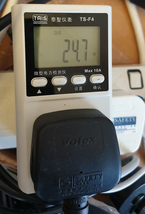
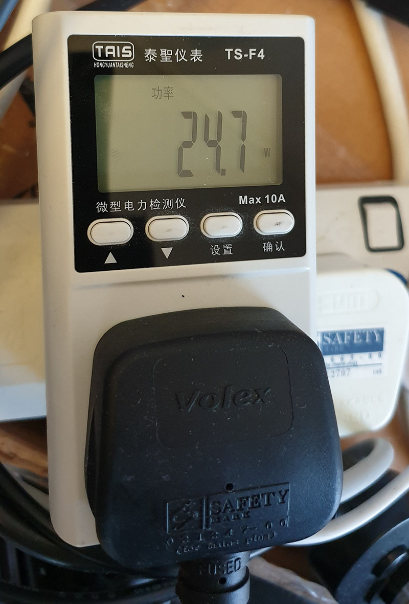
As an aside, ever since I got a smart power meter installed at home, I’ve been trying to eliminate ghost power in the household; by going through my home and systemically shutting down devices that were under-utilized or poorly designed, I’ve managed to cut my power bill by a third. So, I took one of my in-line meters and measured the Form 3’s idle power. It clocks in at around 25 watts, or about 18kWh/mo; in Singapore I pay about US$0.10/kWh, so that’s a $21.60/yr or about 2% of my overall electric bill. I’ve migrated servers and shut them down for less, so probably I’d opt to unplug my Form 3 when it’s not in use, especially since my office is always pretty warm and the heat-up time for the resin would be fairly short.

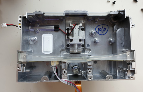
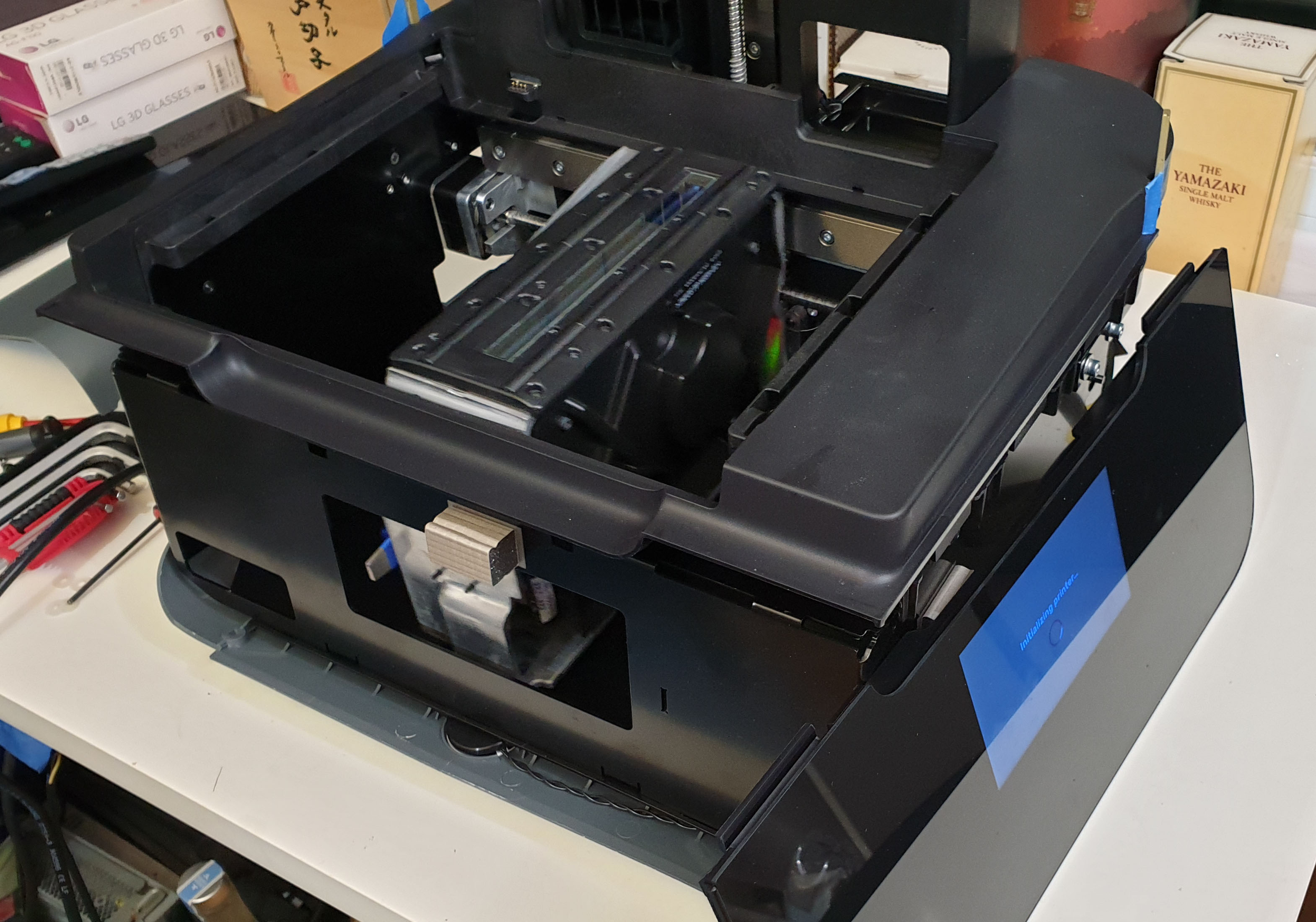
The other thing that set the Form 3 apart from its predecessors is that when I looked inside, there were no optics in sight. Where I had expected to be staring at a galvanometer or mirror assembly, there was nothing but an empty metal pan, a lead screw, and a rather-serious looking metal box on the right hand side. I knew at this point the Form 3 was no incremental improvement over the Form 2: it was a clean-sheet redesign of their printing architecture.

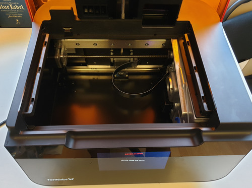
Above: A view into the Form 3 body while idle, revealing nothing but an empty metal box.

I had deliberately avoided exposing myself to any of the press materials on the Form 3 prior to doing the teardown, so that my initial impressions would not be biased. But later on, I came to learn that the serious-looking metal box on the right hand side is called the “Light Processing Unit”, or LPU.

Power cycling the Form 3 quickly revealed that the LPU moves left to right on the internal lead screw. I immediately liked this new design, because it means that you no longer fouled the optics if your build platform dripped while the resin tank was removed. It also meant that the optics were much better sealed and protected, which means that the Form 3 would be much more resistant to smog, fog, and dust than its predecessors.

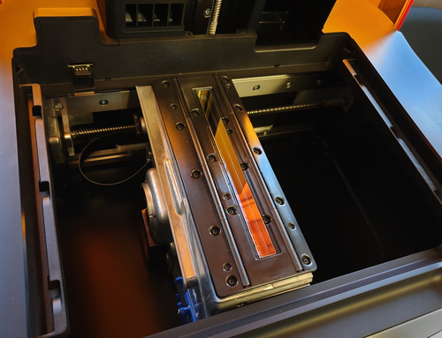
Power cycling the Form 3 causes it to exercise all its actuators as part of a self test, which gives you a nice, unobstructed view of the LPU outside of its stowage position, as shown above. Here, you can see that clearly, the galvanometer scans only in one dimension now, and that the optics look quite well sealed and protected.

▶️

Click the play button to hear the LPU scan

Because the LPU scans in one dimension, and the time it takes for the LPU to complete a scan is variable, the Form 3 makes a sort of “music” when it runs. I recorded a clip of what the LPU sounds like. It has a distinctive whah-whah sound as the servos vary the speed of the LPU as it scans across the print area. At the very conclusion of the short clip, you can hear the high-pitched whine of the LPU doing a “carriage return” across the entire print area. By analyzing the frequency of the sound coming from the LPU, you can infer the rough range of the line scanning rate for the LPU. For the sample I was printing, I get peaks at 23 Hz, 53 Hz, 298 Hz, followed by the carriage-return whine at around 5.2kHz.

Removing the Outer Shell

Taking off the outer panels reveal fabrication methodologies and design techniques that are more aligned with automotive or aerospace design schools than consumer electronics.

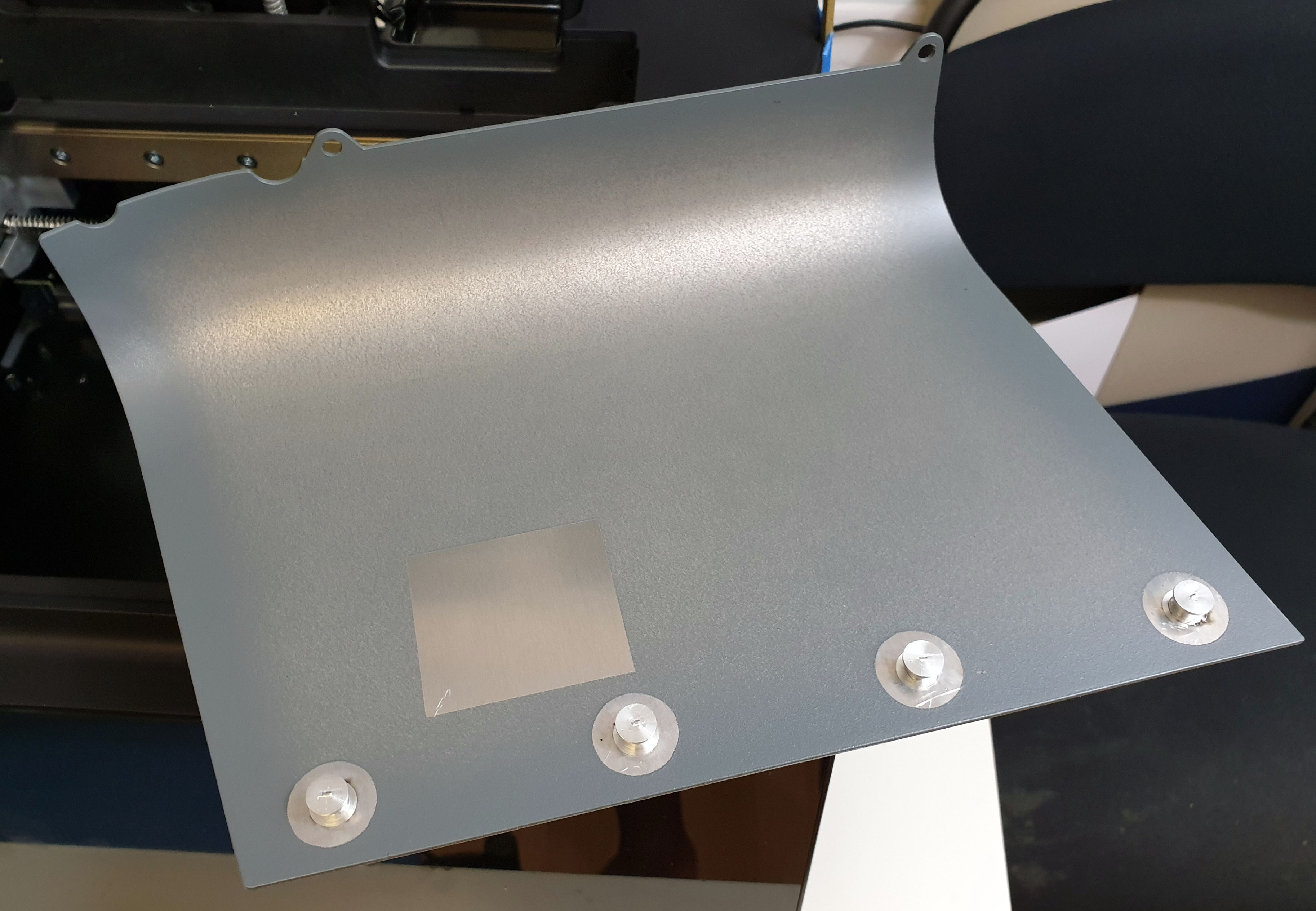
For example, the outer body panels of the Form 3 are made from shaped aluminum sheets that share more in common with the fender of a car than a 3D printer. 1.7mm thick sheet stock is bent into a compound 3D curve using some kind of stamping process, based on the work lines visible on the interior. The sheet then has keyhole fasteners added through a welding process (based on the heat-scoring around the fasteners) and the whole assembly is finally powder-coated.


Above: one of the aluminum “fenders” of the Form 3

This feels overall like a part I’d expect to see on a car or airplane, not on a 3D printer. However, the robustness of the body panels is probably commensurate with the weight of the Form 3 – at 17.5kg or 38.5lbs, it needs some pretty tough body panels to maintain tolerance and shape through shipping and handling.

A bit more wrangling, and the outer clear plastic shells come off. It’s worth noting the sheer size of these parts. They look to be largely molded or cast in one go, with some details like edge flanges glued on as a post-process. Getting a casting to work at this size with this quality is no small trick. There’s no marking on the part to indicate if it’s polycarbonate or acrylic, so I broke off a small corner and burned it. Based on the smell and how it burned, I’m guessing the orange outer case parts are probably cast acrylic.

With a pair of magnets taped to the rear edges of the case to defeat the safety interlocks, I’m able to run the printer with the covers off. Overall, it looks like the printer should be pretty easy to service for basic repairs and calibration in this state. But of course, we must go further…

Front Bezel

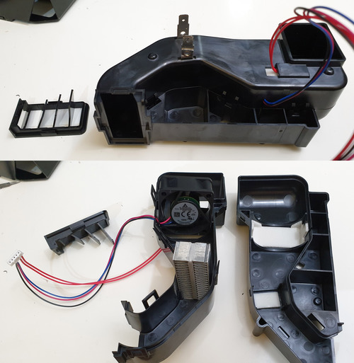
The front bezel of the Form 3 is constructed of a 2mm-thick glass [originally I had thought acrylic] sheet that’s been painted on the inside to create the rectangular opening for the screen. This creates a facade for the printer that recalls the design aesthetic of high-end mobile phones. This clear/painted sheet is then bonded to an ABS superstructure, featuring a robust structural thickness of around 3mm. The 16:9 LCD plus captouch screen is bonded into the clear hole in the acrylic. I’m guessing the resolution of the panel is probably 720p but no more than 1080p, given that the Lontium LT8918 LVDS-to-MIPI repeater embedded in the display’s drive FPC tops out at 1080p/60.

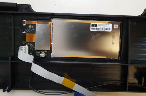
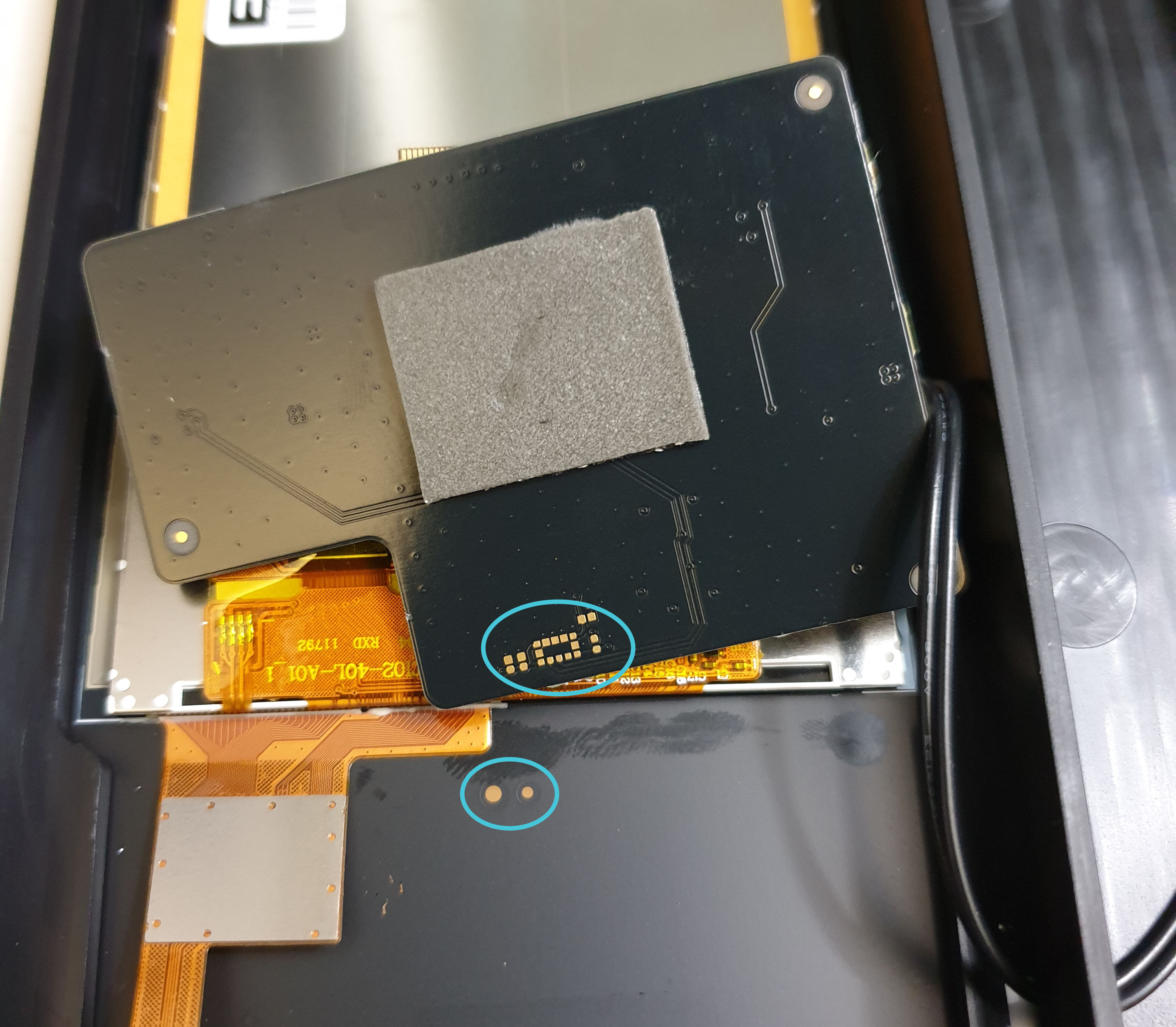
The LCD, touchscreen, and backlight are integrated with the “Display-o-Matic” board, which is held in place using a bit of double-sided tape. Peeling the board off its mounting reveals a small surprise. There’s two apertures cut into the paint next to the screen, along with a 12-LGA footprint that’s not populated. The wiring and empty footprint on the board would be apropos to an ST Microelectronics VL53L0X (or VL53L1X) proximity sensor. This neat little part can detect 1-D gestures up to 4 meters out using time-of-flight laser ranging. I imagine this might have been a candidate for the missing “on/off” switch on the Form 3, but for whatever reason it didn’t make the final cut.

Above: the aperture for the VL53L0X proximity sensor and correspnding empty land patterns on the Display-o-Matic PCB.

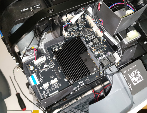
Main Circuit Cluster

The main circuit cluster for the Form 3 is located in the rear right of the printer. After pulling off the case, a set of PCBs comprising the main SoC module and driver electronics is clearly visible. Also note the “roll bar” that spans the rear of the printer – a lot of thought went into maintaining the dimensional stiffness of a fairly massive printer that also had to survive the abuse of a delivery courier.

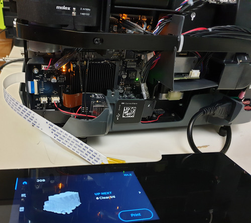
A pair of Molex 2.4/5GHz FPC antennae form a diversity pair for the wifi on the printer. This is a generally good “punt” on RF performance when you have the space to afford a remote antenna: rather than struggling to cram an antenna into a tiny spot, it’s a reasonable approach to simply use a long-ish cable and place freespace-optimized antennae far away from your ground planes, and just hope it all works out. I was expecting to find one antenna oriented horizontally, and the other vertically, to try and capture some polarization diversity, but RF is a complicated thing and maybe other case structures conspired to make two horizontal antennae the best combination for this design.

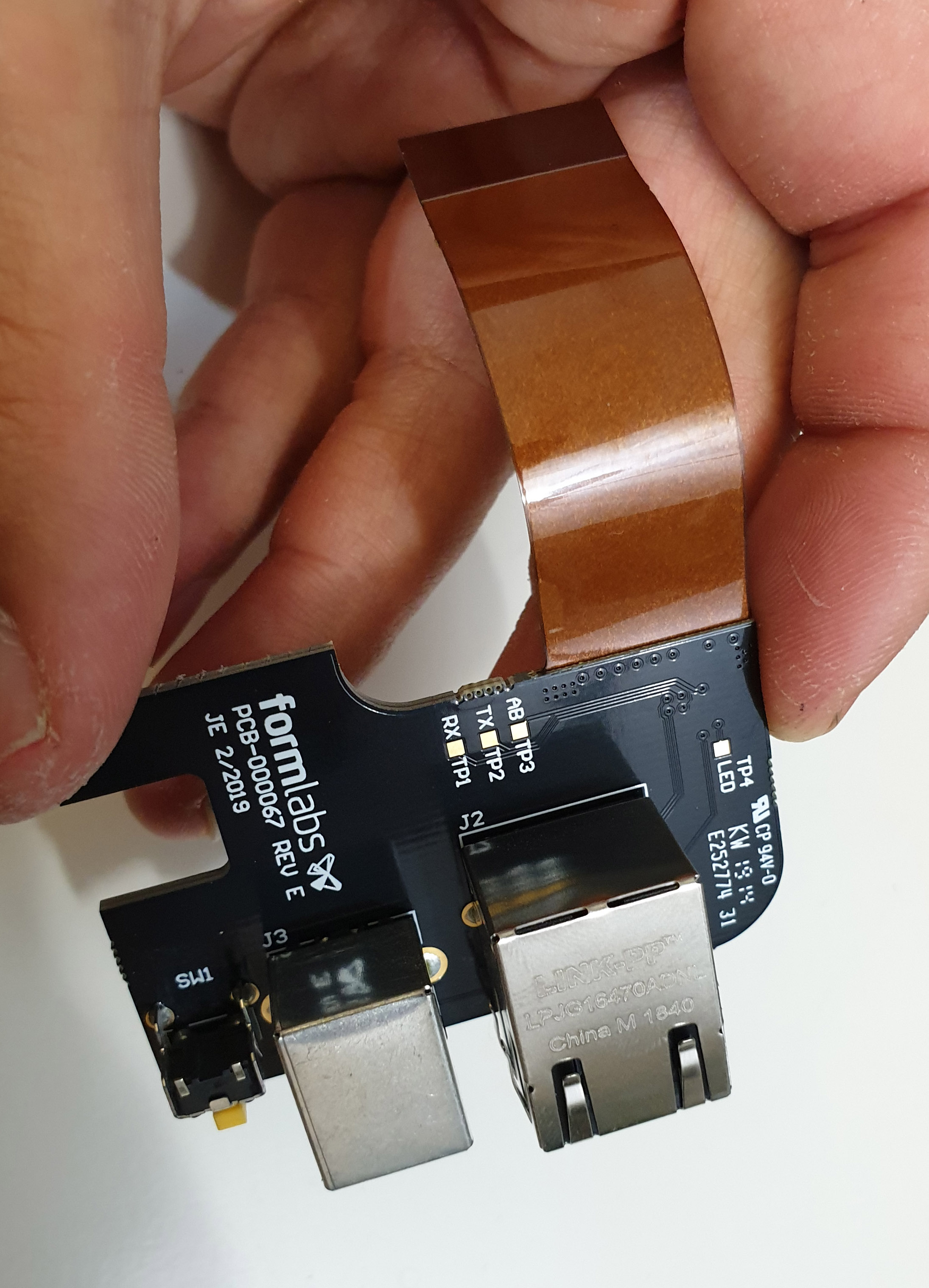
Next to the antennae was another surprise: the Ethernet and USB breakout. The I/O ports are located on a circuit board that mechanically “floats” relative to the main PCB. This probably a blend of design constraint plus concerns about how a circuit board might fare as the most rigid element bridging a flexible polymer case to a rigid steel core in a 17.5kg product that’s subject to drop-kicking by couriers.

That the I/O ports are on its own PCB isn’t so strange; it’s the construction of that PCB and connector that is remarkable.

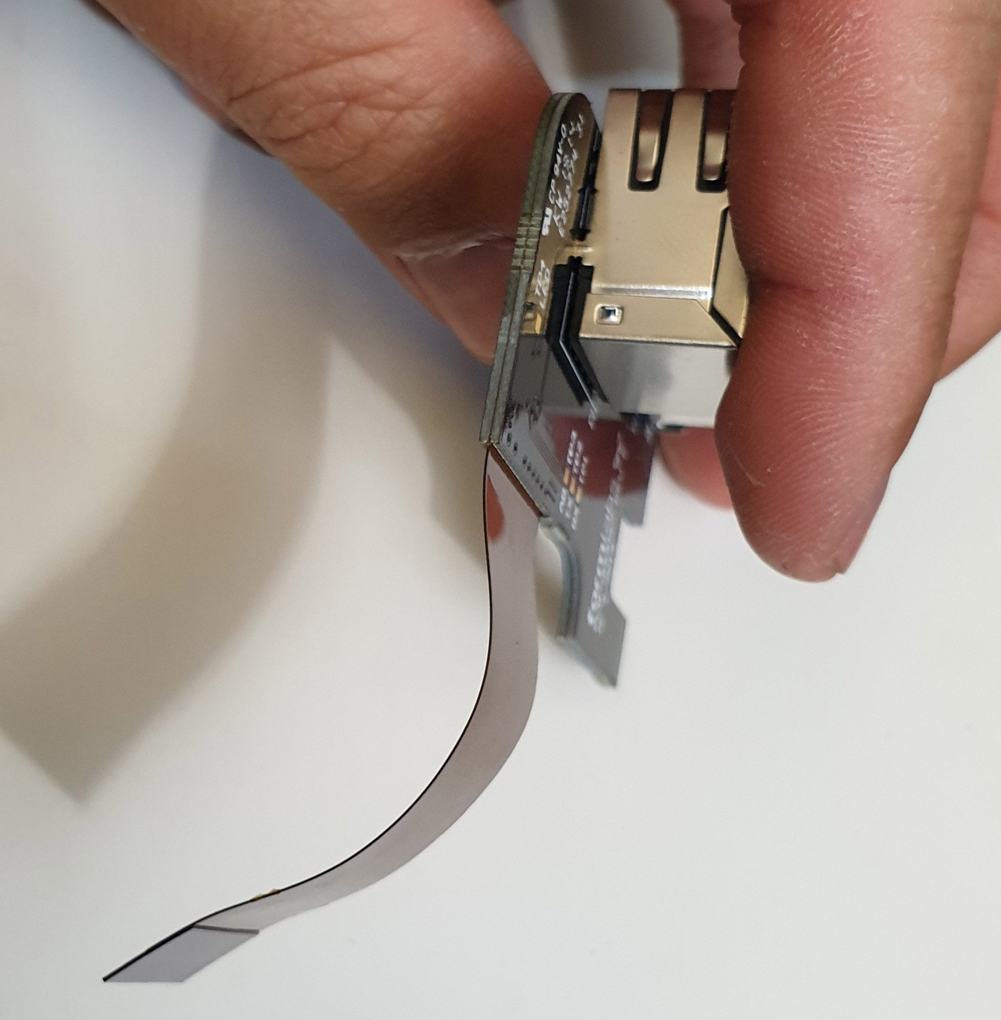
The breakout board is a rigi-flex PCB. This is perhaps one of the most expensive ways I can imagine implementing this, without a ton of benefit. Usually rigi-flex PCBs are reserved for designs that are extremely space-constrained, such that one cannot afford the space of a connector. While the USB2.0 speeds at 480Mbps are fast (and the Gigabit ethernet is even slower at 4x250Mbps diff pairs), it’s not so fast that it requires a rigi-flex PCB for impedance control; in fact, the opposing side is just a regular FPC that snaps into a rather unremarkable FPC connector (there are more exotic variants that would be invoked if signal integrity was really an issue). The flex portion does look like they’ve embedded a special solid conductor material for the reference plane, but normally one would just build exactly that – a flex cable with a reference plane that otherwise goes into two plain old FPC connectors.

Perhaps for some bizarre reason they couldn’t meet compliance on the USB connection and instead of re-spinning all of the main electronics boards they bought margin by using a Cadillac solution in one portion of the signal chain. However, I think it’s more likely that they are contemplating a more extensive use of rigi-flex technology in future iterations, but because there are relatively few reliable suppliers for this type of PCB, they are using this throw-away board as a “walk before you run” approach to learn how to work with a new and potentially difficult technology.

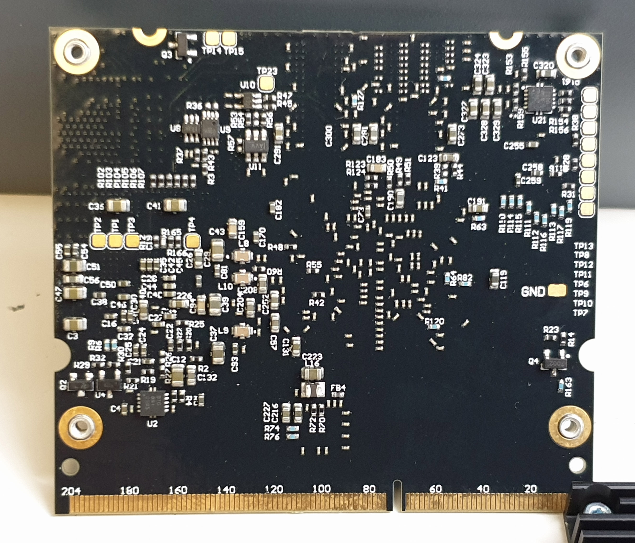
Turning from the I/O connectors to the main board, we see that like the Form 2, the Form 3 splits the system into a System-on-Module (SOM) plugged into a larger breakout board. Given the clearly extensive R&D budget poured into developing the Form 3, I don’t think the SOM solution was chosen because they couldn’t afford to build their own module; in fact, the SOM does bear a Formlabs logo, and uses a silkscreen font consistent with Altium, the design tool used for all the other boards. Unlike their other boards, this PCB lacks the designer’s initials and a cute code name.

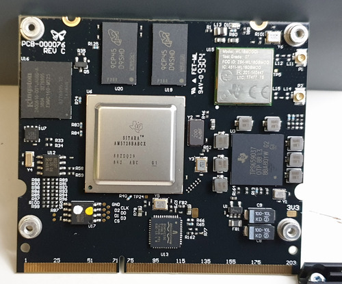
My best guess is that this is somewhere in between a full-custom Formlabs design and an off the shelf OEM module. The position of the components are quite similar to those found on the Compulab CL-SOM-AM57x module, so probably Formlabs either licensed the design or paid CompuLab to produce and qualify a custom version of the SOM exclusively for Formlabs. For a further discussion of the trade-offs of going SOM vs fully integrated into a single PCB, check out my prior teardown of the Form 2. The TL;DR is that it doesn’t make economic sense to combine the two into a single board because the fine trace widths and impedance control needed to route the DDR memory bus on the CPU is wasted on the much larger bulk of the control PCB, along with other ancillary benefits of being able to modularize and split up the rather complex supply chain behind building the SOM itself.

The control breakout board once again relies on an STM32 CPU to do the real-time servo control, and Trinamic motor drivers. Thus from the perspective of the drive electronics and CPU, the Form 3 represents an evolutionary upgrade from the Form 2. However, this is about the only aspect of the Form 3 that is evolutionary when compared to the Form 2.

A Shout-Out to the Power Supply

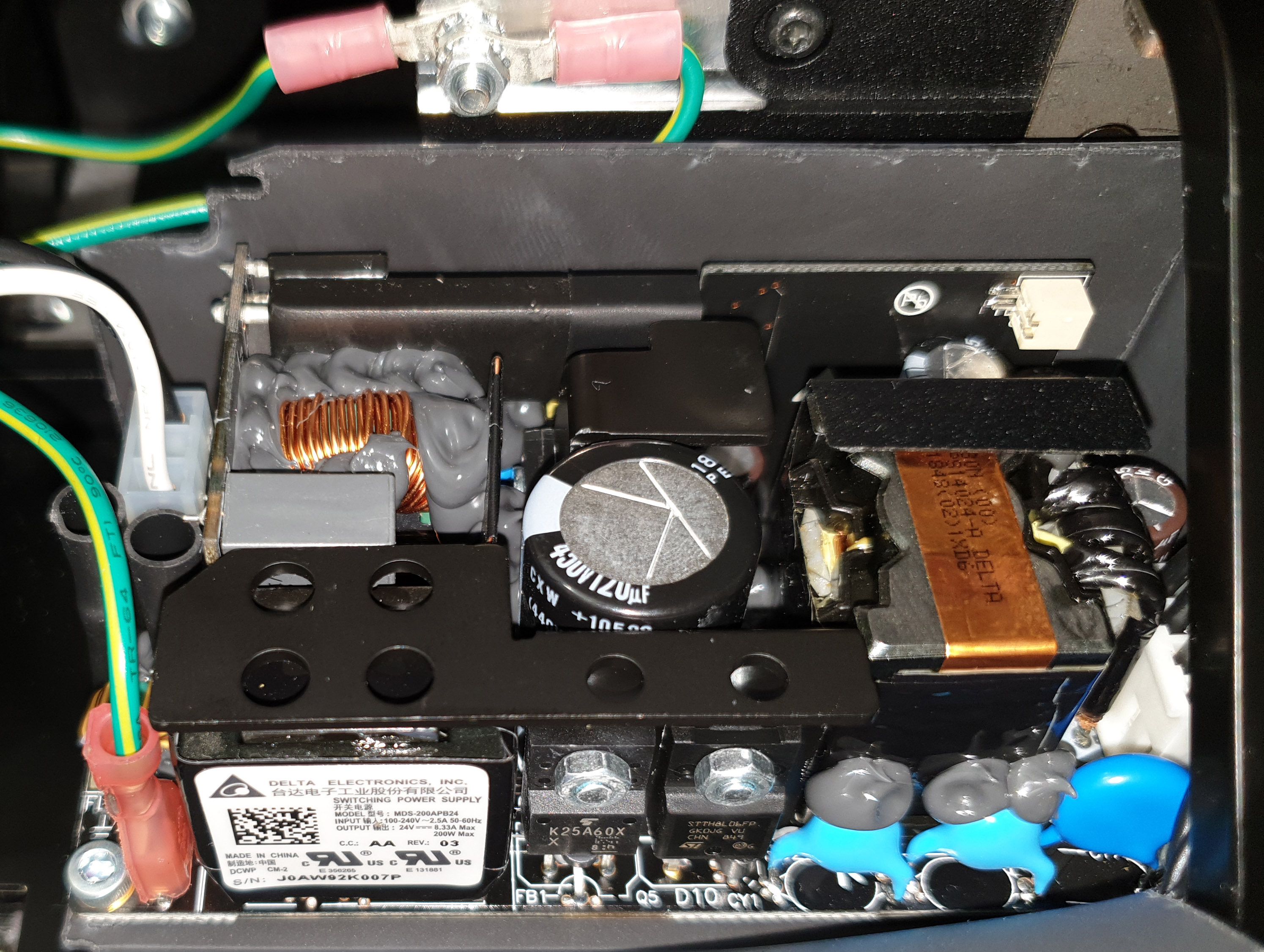
The power supply: so humble, yet so under-appreciated. Its deceptively simple purpose – turning gunky AC line voltage into a seemingly inexhaustable pool of electrons with a constant potential – belies its complexity and bedrock role in a system. I appreciate the incorporation of a compact, solid, 200W, 24V @ 8.33A power supply in the Form 3, made by a reputable manufacturer.

Measuring Resin

The Form 2 had no real way of knowing how much resin was left in a cartridge, and it also used this wild projected capacitive liquid level sensor for detecting the amount of resin in the tank. When I saw it, I thought “wow, this has got to be some black magic”.

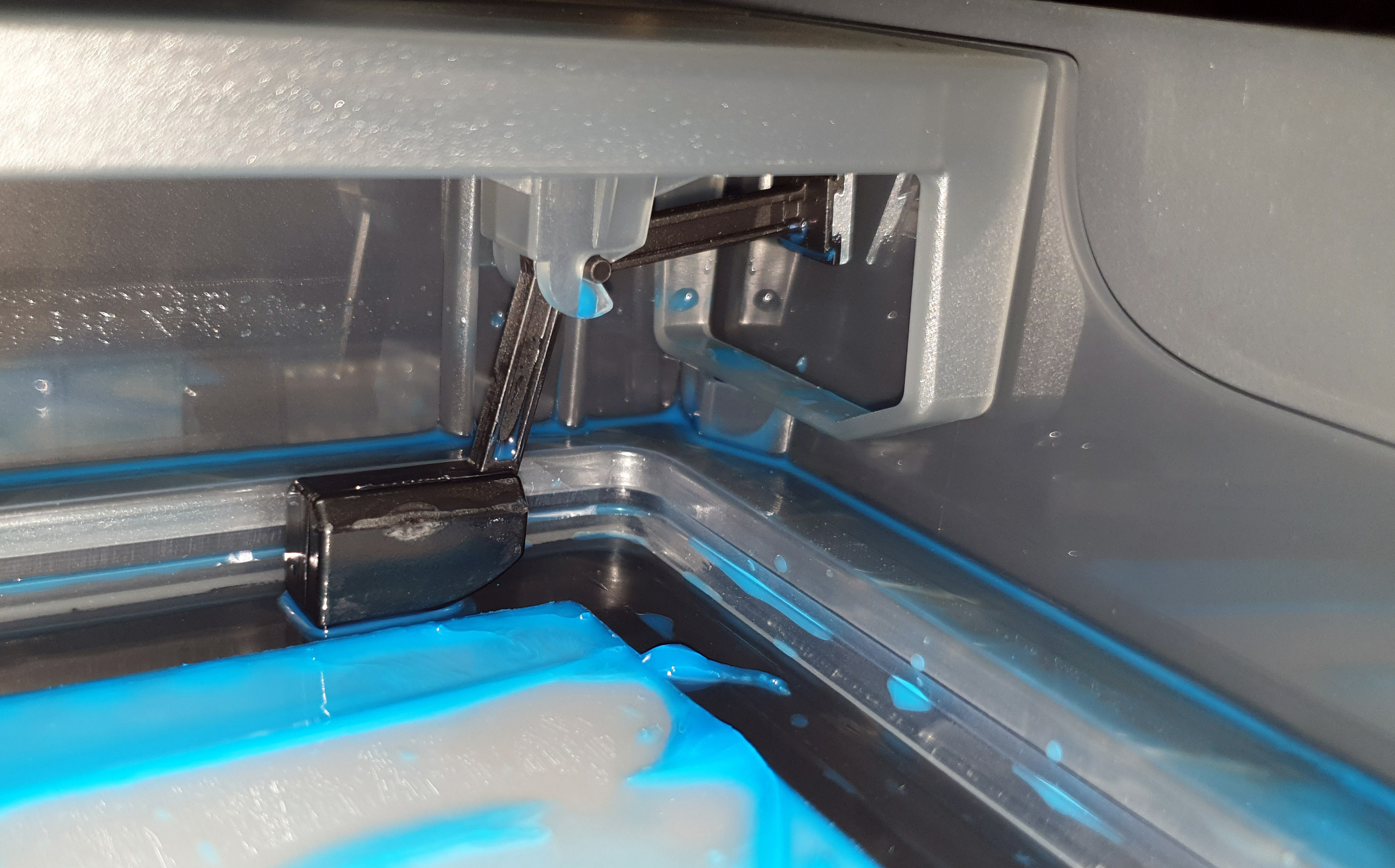
The Form 3 moves away from using a capacitive sensor – which I imagine is pretty sensitive to stray fields, humidity, and the varying material properties of the resin itself – to a mechanical float inside the tank.

One end of the float sits in the resin pool, while the other swings a small piece of metal up and down. My initial thought is that this bit of metal would be a magnet of some sort whose field is picked up by a hall effect sensor, except this introduces the problem of putting calibrated magnets into the resin tray.

It turns out they didn’t use a magnet. Instead, this bit of metal is just a lump of conductive material, and the position of the metal is sensed using an LDC1612 “inductance-to-digital” converter. This chip features a 28(!) bit ADC which claims sub-micron position sensing and a potential range of greater than 20cm. I didn’t even know these were a thing, but for what they are looking to do, it’s definitely a good chip for the job. I imagine with this system, there should be little ambiguity about the level of resin in the tank regardless of the environmental or dielectric properties of the resin. Variations in density might change the position of the float, but I imagine the float is so much more bouyant than the resin, so this variable would be a very minor factor.

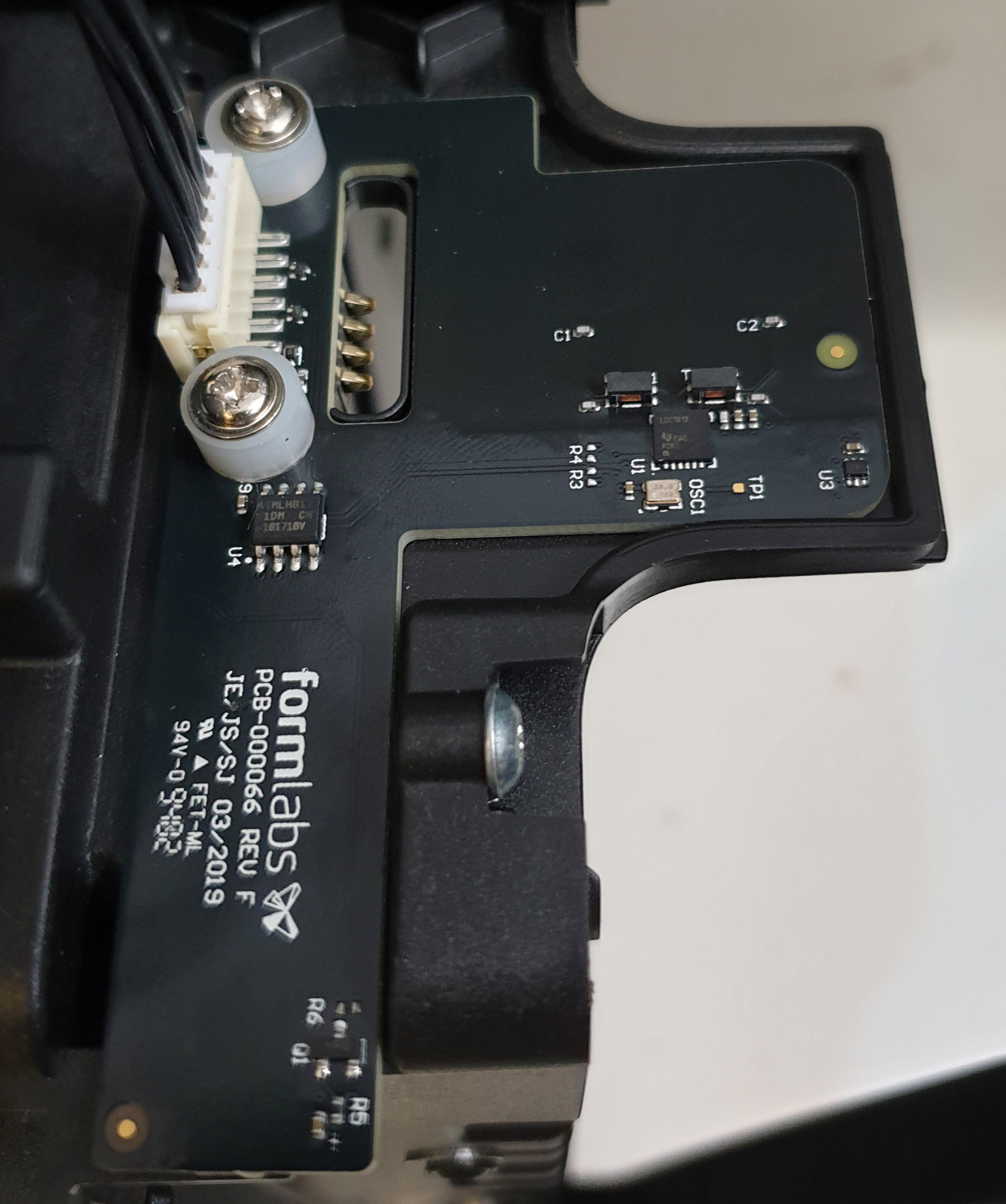
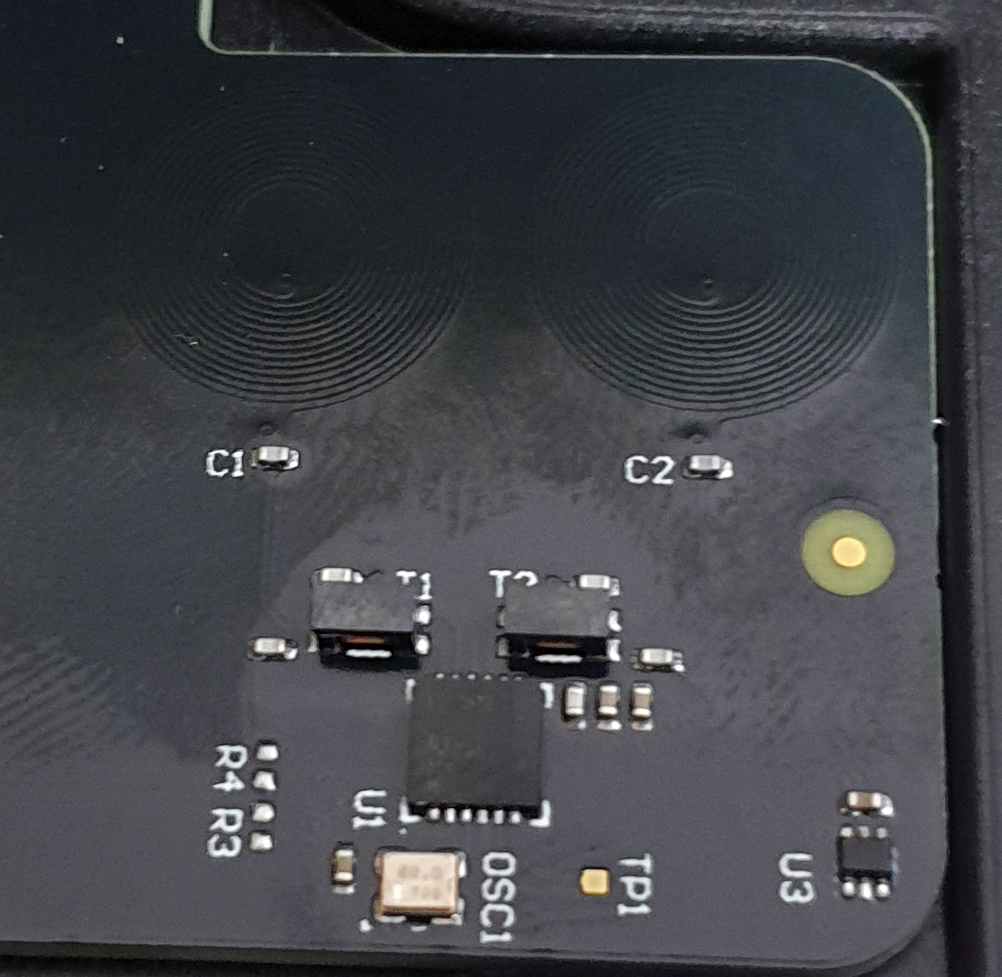
The LDC1612 and its companion spiral PCB traces sit on a small daughtercard adjacent to the resin tank.

While the LDC1612 lets the Form 3 know how much resin is in the tank, but it still doesn’t answer the question of how much resin is left in the cartridge. The Form 3’s resin cartridge format is identical to the Form 2 (down to the camelback-style “bitevalve” and shampoo-cap air vent), so it seems modifying the cartridge was out of question. Perhaps they could have gone for some sort of capacitive liquid-level sensing strip running down the length of the device, but as mentioned above, capacitive sensors are fussy and subject to all sorts of false readings, screening problems and interference.

The Form 3’s solution to this problem is to incorporate a load cell into the resin cartridge mounting that weighs the resin cartridge in real-time. That’s right, there is a miniature digital scale inside every Form 3!

This is what the underside of the “digital scale” looks like. The top metal plate is where the resin tank sits, and the load cell is the silvery metal bar with a pair of overlapping holes drilled out of it on the right. The load-bearing connection for the top metal plate is the left hand side of the load cell, while the right hand side of the load cell is solidly screwed into the bottom metal plate. You can squeeze the two plates and see the top plate deflect ever so slightly. Load cells are extremely sensitive; this is exactly the sensor used in most precision digital scales. Accuracy and repeatability down to 10’s of milligrams is pretty easy to achieve with a load cell, so I imagine this works quite nicely to measure the amount of resin left in the tank. Just be sure not to rest any objects on top of your resin cartridge, or else you’ll throw off the reading!
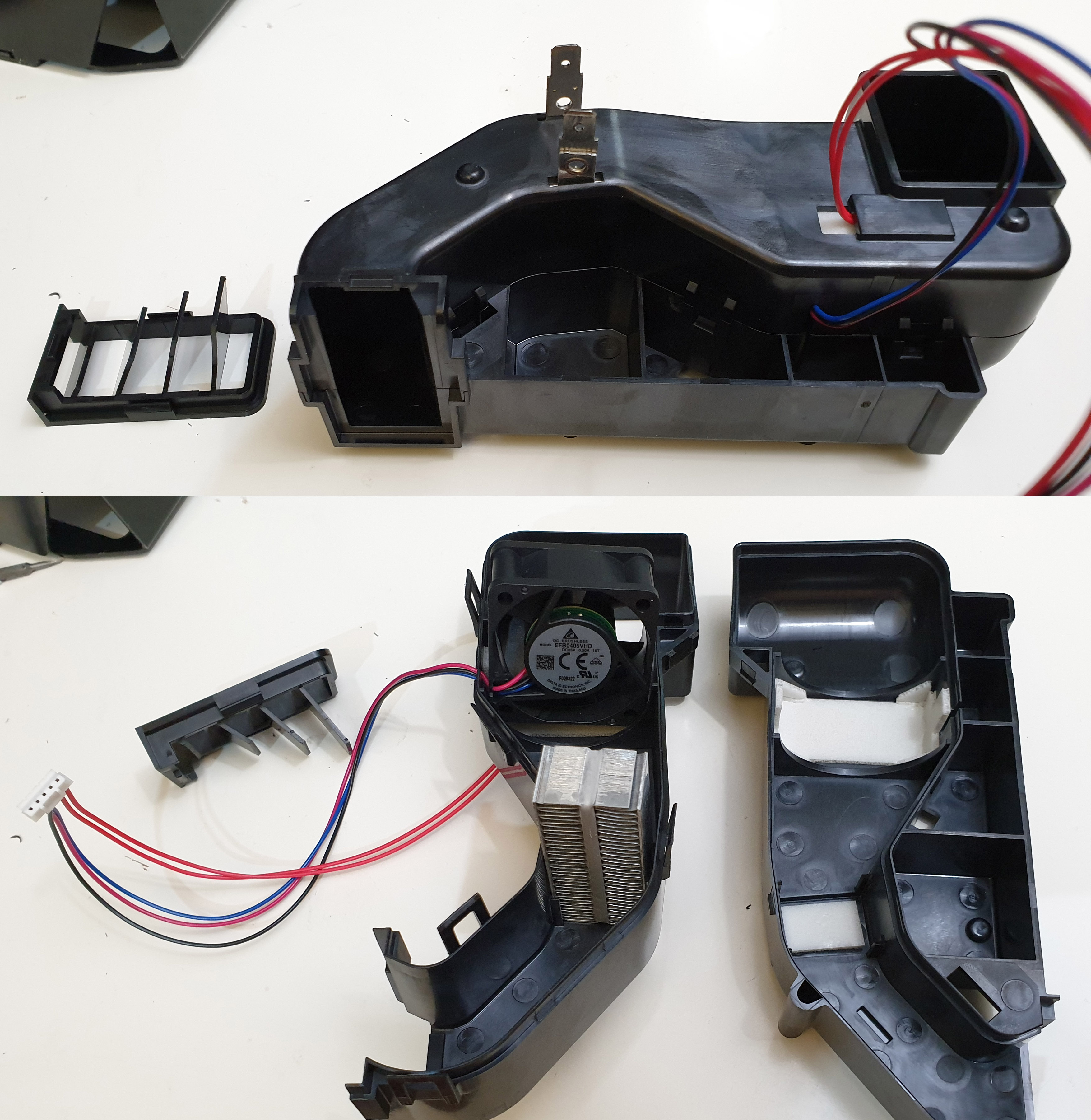
Heating the Resin

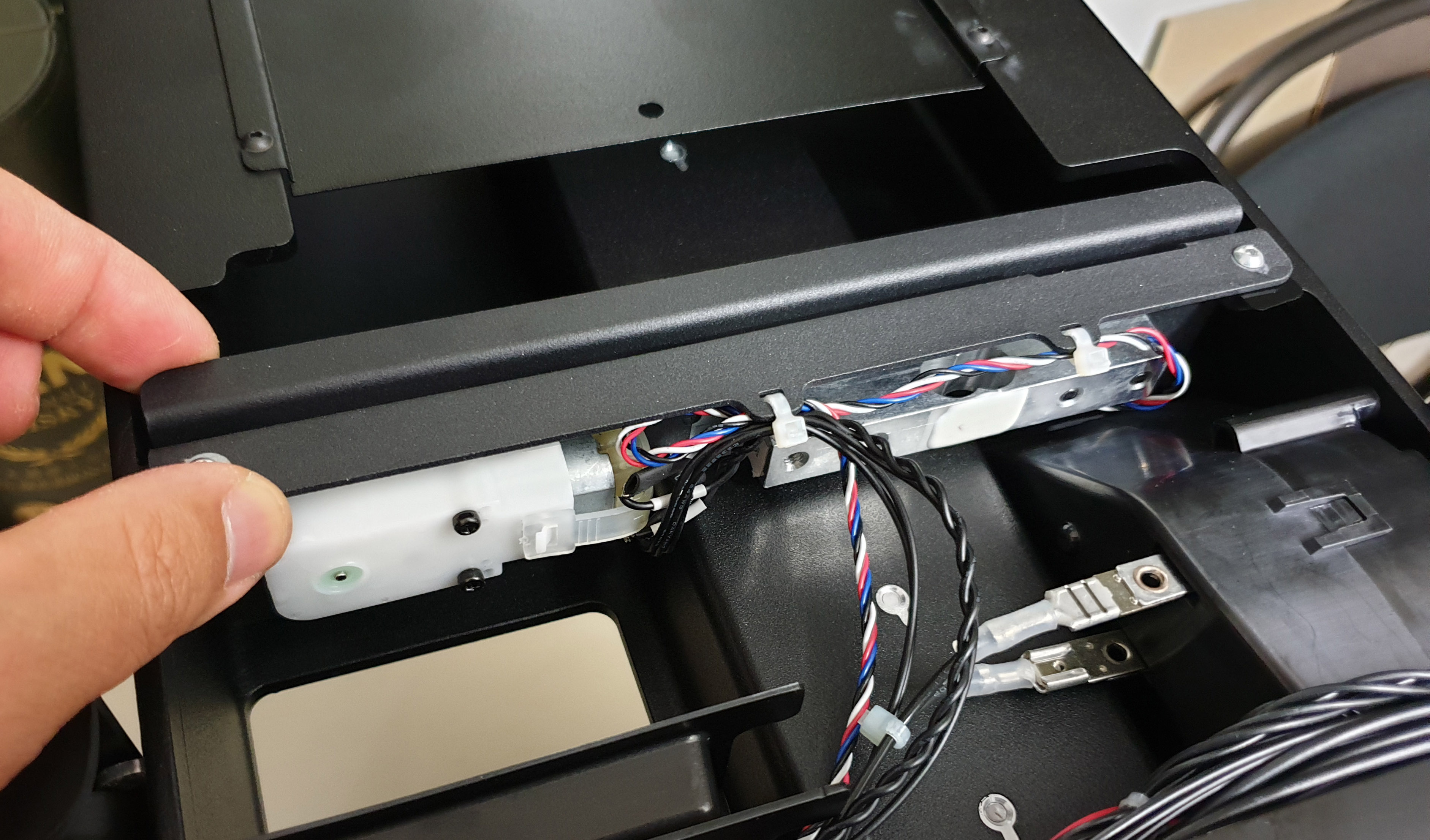
In addition to measuring the resin levels, the Form 3 also needs to heat it. It seems the resin works best at slightly above normal room temperature, around 30C; and unless you live in Singapore, you’re going to need something to heat up the resin. The Form 2 used a nifty PCB-turned-heater around the resin tank. The Form 3 abandons this and incorporates basically a hair dryer inside the printer to heat the resin.

The hairdryer – erm resin heater – exhausts through a set of louvers to the left of the printer’s spine. The air is heated by a 120W, 24V heating element. I imagine they may not run it at a full 120W, but I do have to wonder how much of the Form 3 power supply’s 200W rating is budgeted to this one part alone. The “hairdryer” draws air that is pre-heated by the internal electronics of the Form 3, which may explain why the printer lacks an on/off button: assuming they had a goal of keeping the resin warm at all times, shutting down the main electronics just to turn it on again and then burn a 100+ watts to heat up your resin in a hurry doesn’t make much sense and is a bad user experience. I do like the elegance of recycling the waste heat of the electronics for a functional purpose; it makes me feel a little less bad that there is no way to put the printer into an apparent sleep mode.

The LPU

Now it’s time to get into the main act! The Light Processing Unit, or LPU, is the new “engine” of the Form 3. It’s the solid looking metal box that parks on the right hand side of the Form 3 when it’s idle, and scans back and forth across the print area during printing.

The LPU is a huge departure from the architecture of the previous Form 1 and 2 printers. The original Form printers used two galvanometers in series to create a 2-D laser scanning pattern. The total moving mass in this architecture is quite small. The theory behind the galvo-only design was that by relying just on the mesoscopic mass of the galvanometers, you can scan a laser to arbitrary points on a build stage, without being constrained by the physics of moving a macroscopic object like a print head: with a mechanical bandwidth on the order of 10kHz, a laser dot’s position can be shifted in a fraction of a millisecond. This also cuts back on large, heavy stepper motors, yielding a more compact design, and in some ways probably made the overall printer more forgiving of mechanical tolerances. The alignment features for all the critical optics could be machined into a single block, and any optics-to-build-stage alignment could theoretically be calibrated and “computed out” post-assembly.

However, in practice, anyone who has watched a Form print using a clear resin has probably noticed that the laser scan pattern rarely took advantage of the ability to take arbitrary paths. Most of the time, it scans across the build platform, with a final, quick step that traces the outlines of every build slice.

So why change the design? Although galvanometers can be expensive, having done a couple tear-downs of them I’m of the belief their high price is mostly reflective of their modest volumes, and not any fundamental material cost. After all, every mechanical hard drive shipped contains a voice coil capable of exquisite positioning resolution, and they don’t cost thousands of dollars. So it’s probably not a cost issue.

Other downsides of the original galvo-only construction include the laser beam taking an increasingly eccentric oval shape the further it gets off-axis, causing print resolution to be non-uniform across the build platform, and the active optics area being equivalent to the entire area under the build platform, meaning that resin drips and dust on the glass can lead to printing defects. The LPU architecture should, presumably, solve this problem.

Probably the biggest hint as to why the change is the introduction of the Form 3L: it roughly doubles the size of the build platform, while maintaining throughput by slaving two LPU’s in parallel. While it may be possible to tile 2-D galvanometer setups to increase the build platform size without reducing throughput, it would require stitching together the respective light fields of multiple galvanometers, which may be subject to drift over time. However, with the LPU, you could in theory create an arbitrarily long build platform in one axis, and then plug in more LPUs in parallel to improve your printing speed. Because they are all connected to the same mechanical leadscrew, their tolerances should drift together, leading to a robust and repeatable parallel printing architecture. The LPU architecture is extremely attractive if your company has a long-term vision of making 3D printing a mass production-capable process: it gives you more knobs to turn to give customers willing to pay a lot up front to improve their build throughput and/or latency. One could even imagine doubling the width of the build area by placing a second, opposite lead screw and interdigitating the LPUs.

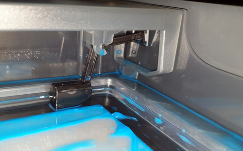
It’s also worth mentioning that the introduction of the LPU has lead to a significant redesign of the resin tank. Instead of a silicone-based “peel” system, they have gone to a compound material system that gives them a flexible membrane during the “pull” step between layers, and a rigid platform by tensioning a hefty clear plastic sheet during the “print” phase. My gut tells me that this new platform also gives them a scaling path to larger build volumes, but I don’t know enough about the physics of what happens at the interface of the resin and the build stage to know for sure the trade-offs there.

The LPU also incorporates a number of other improvements that I think will have a huge impact on the Form 3’s overall performance and reliability:

• Because the galvo only needs to scan in 1 dimension, they are able to use a parabolic mirror to correct for the angle of the beam relative to the build platform. In other words, they are able to maintain a perpendicular, circular beam spot regardless of the build platform location, eliminating the loss of resolution toward the edges that a 2-D scanning system would suffer.
• The entire LPU is environmentally sealed. My Form 1 printer definitely suffered from a build-up of tiny particulates on the mirrors, and I’m dreading the day I have to clean the optics on my Form 2. While in theory they could have sealed the galvanometers of the Form 2, there’s still the huge build mirror and platform window to deal with. The LPU now has a single optical surface that looks trivial to wipe down with a quality lens cloth.
• The LPU can be “parked” during shipping and maintenance. This means zero risk of resin dripping on sensitive optical surfaces.
• The LPU is a separate, value-add module from the rest of the printer, allowing Formlabs to invest more heavily in the development of a critical component. It also opens up the possibility that Formlabs could OEM the LPU to low-cost manufacturers, allowing them to create a price-differentiated line of printers with less risk to their flagship brand name, while retaining a huge amount of control over the ecosystem.

The main downsides of the LPU, I imagine, are its sheer size and mass, and what appears to be an extremely tight mechanical tolerance spec for the alignment of the LPU relative to the build platform, both of which drive the overall size and mass of the system, presumably also driving up costs. Also, if you’re thinking ahead to the “millions” volumes of printers, my gut says the LPU is going to have a higher cost floor than a 2D galvo system. When you get to the point where tooling and R&D is fully amortized, and production yields are “chasing 9’s” (e.g. 99.9…%), you’re now talking about cost in terms of sheer bulk and mass of materials. It’s also more difficult in general to get good tolerance on large assemblies than small ones, so overall the LPU looks like a bet on quality, build volume scalability, and faster print times, at the expense of the overall potential cost floor.

OK, enough yammering, let’s get hammering!

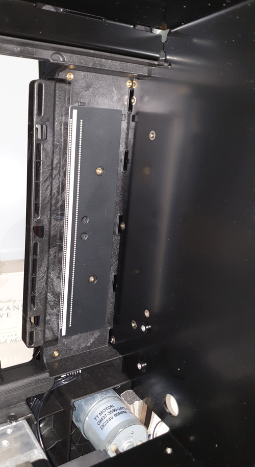
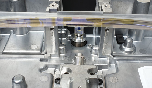
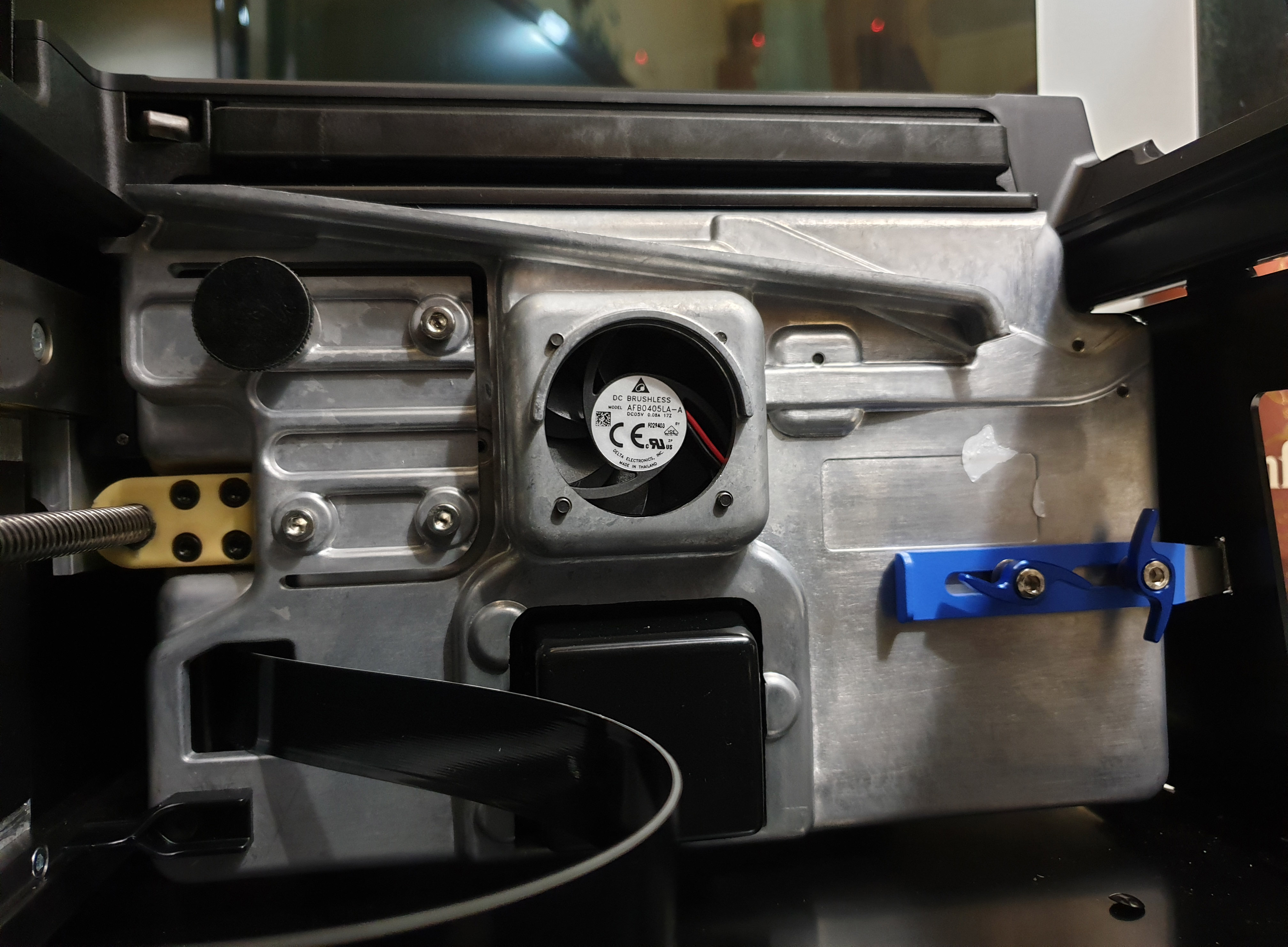
This is a view of the LPU as-mounted in the printer, from the inside of the printer. On the left, you can see the lead screw responsible for shuttling the LPU back and forth. Just next to that you can see an array of three large silver screws and one large black thumb screw, all mounted on a cantilever-type apparatus. These seem to be used to do a final, critical alignment step of the LPU, presumably to get it to be perfectly perpendicular once all mechanical tolerances are accounted for. On the right hand side, there’s a blue anodized latching mechanism. I’m not sure what it’s for – my Form 3 arrived in a special shipping case, but perhaps on consumer units it’s meant to secure the LPU during shipping, and/or it’s used to assist with servicing and alignment. In the middle-bottom, you can see the protective cover for the galvonometer assembly, and of course the cooling fan for the overall LPU is smack dab in the middle.

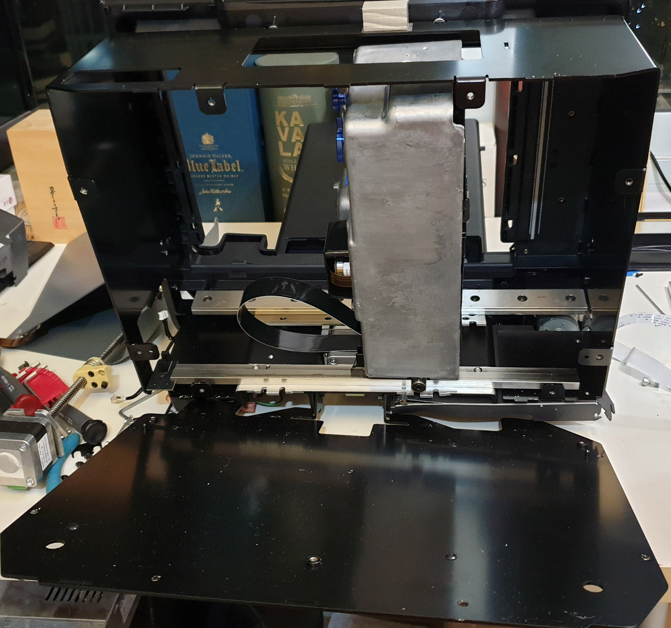
I had to struggle a bit to extract the LPU. Eventually I figured out that the bottom plate of the printer can be detached, giving easy access to the LPU and its attached linear carriage.

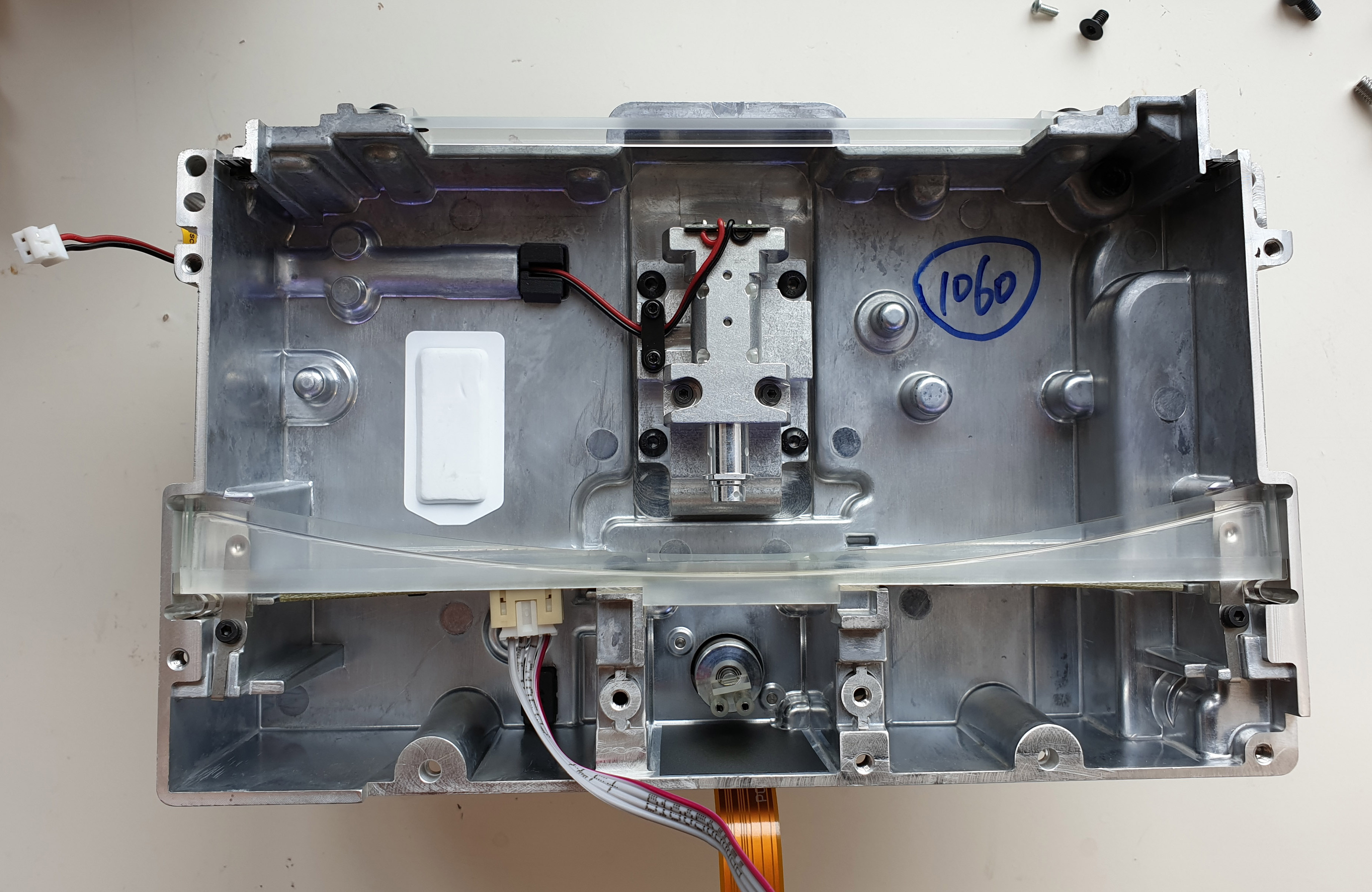
The inside view of the Form 3 from the bottom-up also reveals the details of the calibration standard placed near the LPU’s parking spot. The calibration standard looks like it covers the entire build area, and it looks like it contains sufficient information to correct for both X and Y offsets, and the reflective-vs-matte coating presumably helps to correct for laser amplitude drift due to laser aging as well. I was a little surprised that the second dot pattern wasn’t a vernier of the first to increase the effective spatial resolution of the calibration pattern, but presumably this is sufficient to do the job. You can also see the hefty 24V motor used to pull the tensioning film on the resin tank, and the texture of the plastic body betrays the fact that the polymer is glass-filled for improved rigidity under these heavy loads.

There seems to be no graceful way to pull the LPU out without also bringing its linear carriage along for the ride, so I took both parts out as a single block. It’s a pretty hefty piece, weighing in at 2.5kg (5.6lb) inclusive of the carriage. Fortunately, the bulk of the mass is supported by a circular bearing on a rail beneath the carriage, and the actual absolute rate of acceleration required for the block isn’t so high as it is intended to scan in a smooth motion across the build surface.

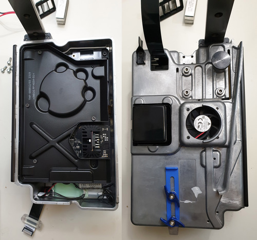
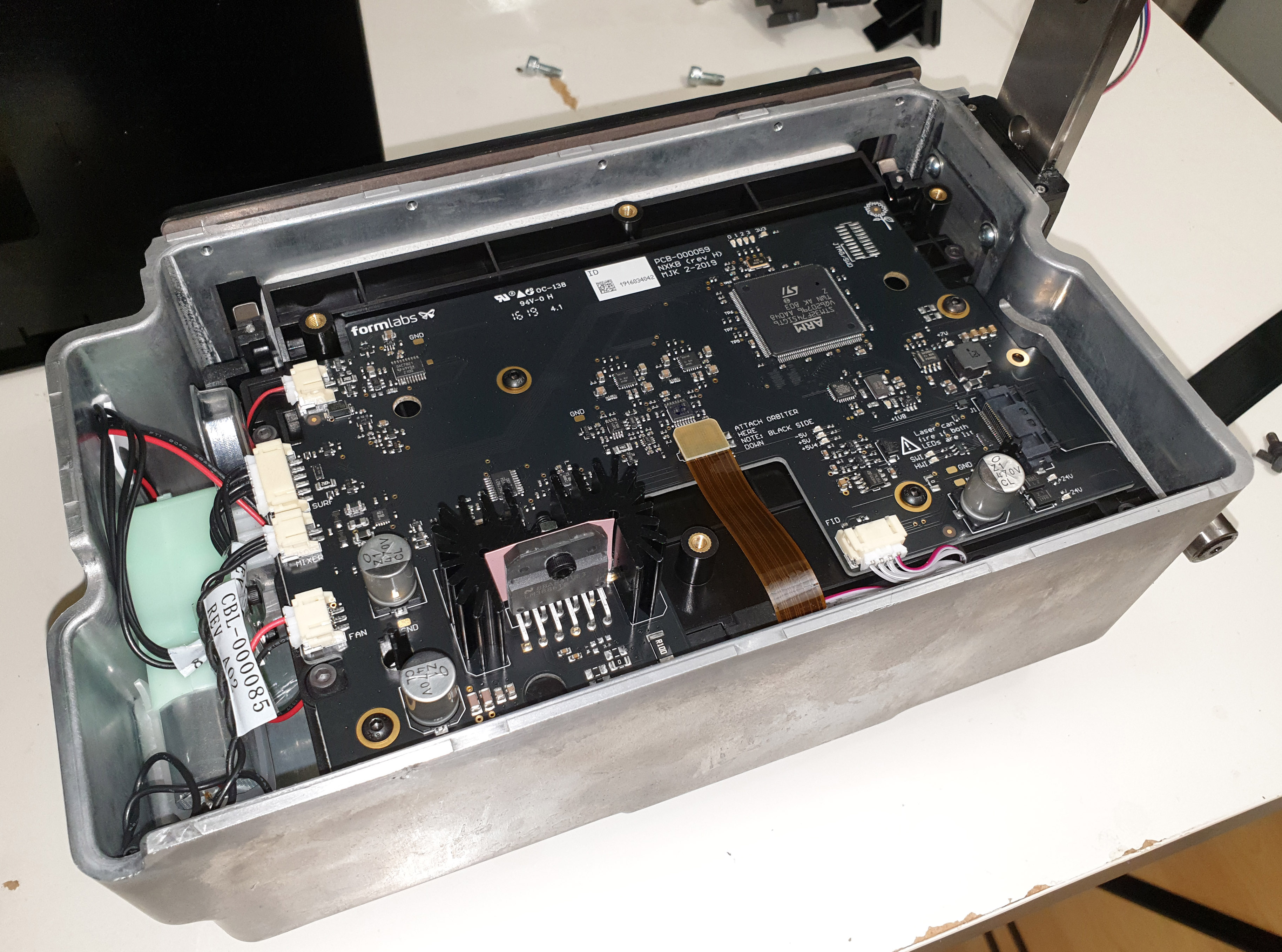
Above is the LPU plus its linear carriage, now freed of the body of the Form 3. The die cast aluminum case of the LPU is reminiscent of an automotive ECU; I wouldn’t be surprised if a tour through the factory producing these cases revealed car parts rolling down a parallel line to the Form 3’s LPU case.

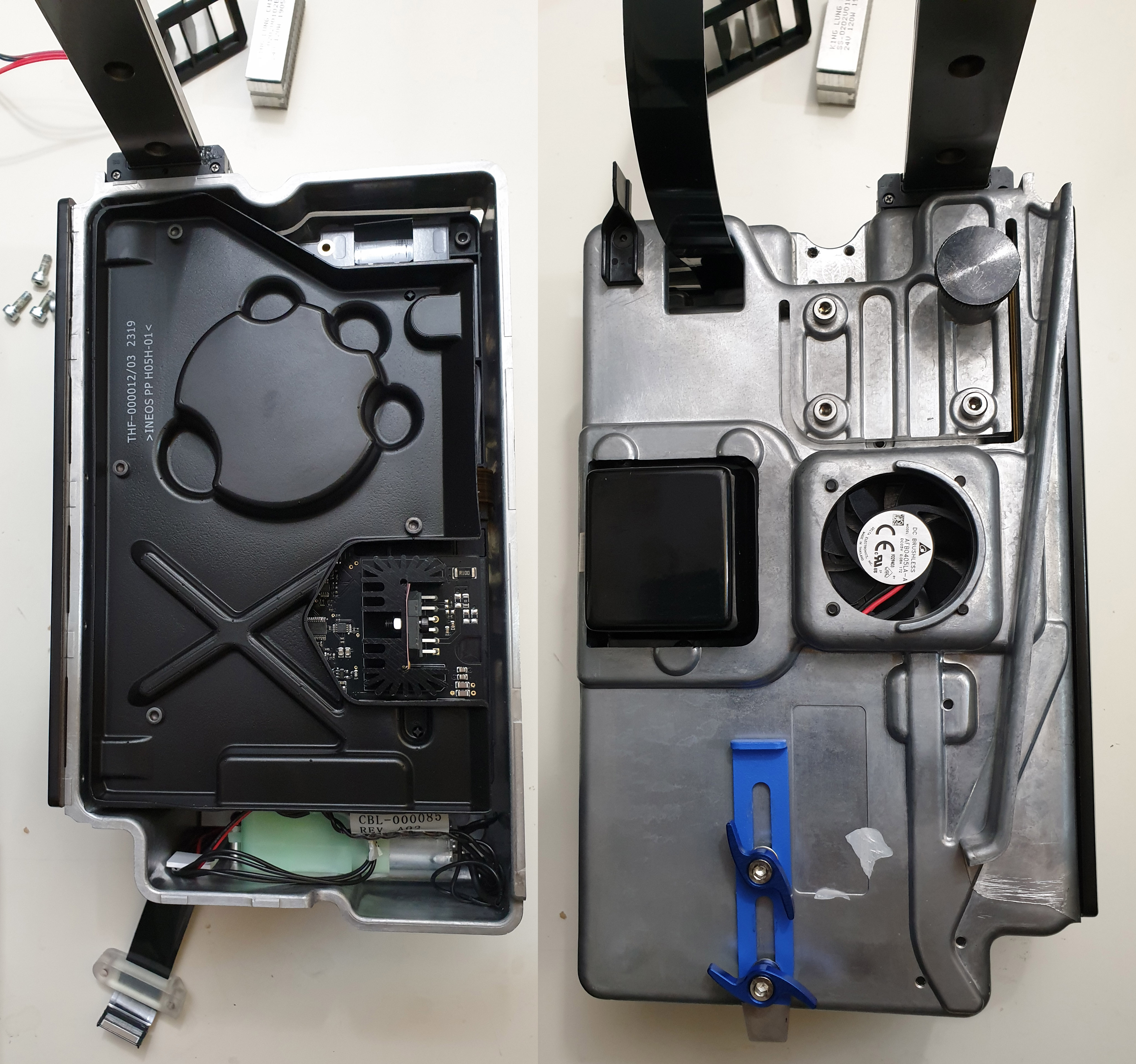
Removing the black polypropylene protective cover reveals the electronics baked into the LPU. There’s an STM32F745 Cortex-M7 with FPU, hinting that perhaps the LPU does substantial real-time processing internally to condition signals. An SMSC 332x USB PHY indicates that the LPU presents itself to the host system as a high-speed USB device; this should greatly simplify software integration for systems that incorporate multiple, parallel LPUs.

Aside from a smattering of analog signal conditioning and motor drivers, the board is fairly bare; mass is presumably not a huge concern, otherwise I’d imagine much of the rather dense FR-4 material would have been optimized out. I also appreciated the bit of aerospace humor on the board: next to the flex connector going to the galvanometer are the words “ATTACH ORBITER HERE / NOTE: BLACK SIDE DOWN”. These are the words printed on the struts which attached the Space Shuttle to the Shuttle Carrier Aircraft – a bit of NASA humor from back in the day.

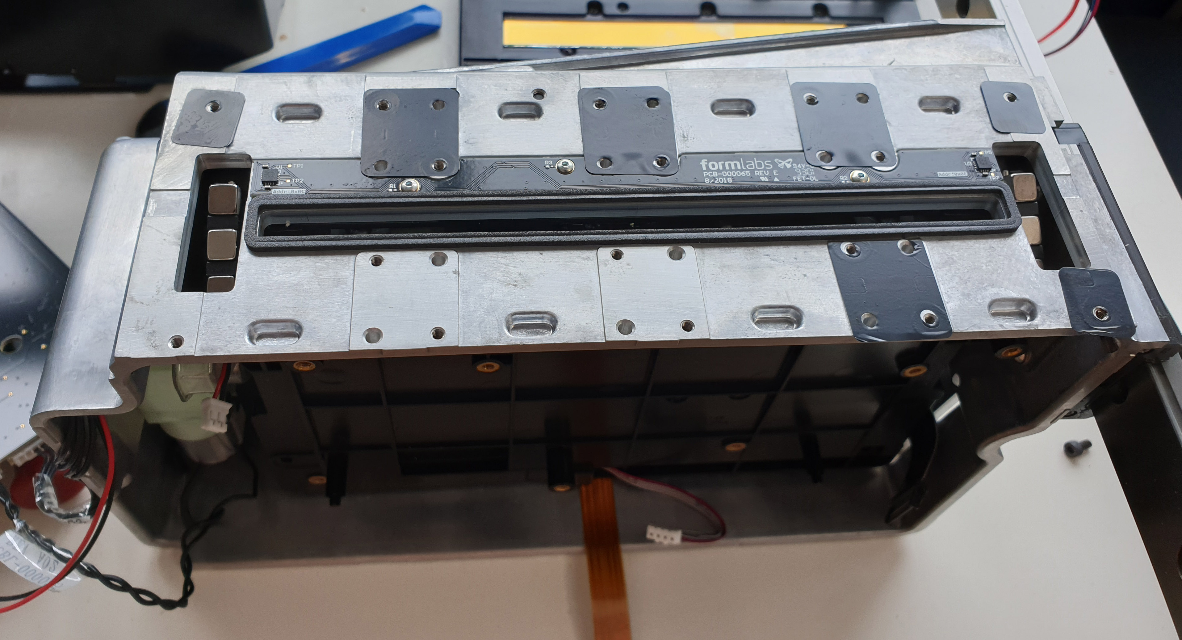
Removing the mechanical interface between the LPU and the resin tank reveals a set of 2×3 high-strength magnets mounted on rotating arms that are used to pull the resin stir bar inside the tank, along with a pair of MLX90393 3-axis hall-effect sensors providing feedback on the position of the magnets.

Pulling the electronics assembly out of the LPU housing is a bit of a trick. As noted previously, the optics assembly is fully-sealed. Extracting the optical unit for inspection thus required cutting through a foam tape seal between the exterior glass plate and the interior sterile environment.

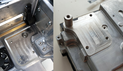
Thus freed, we can see some detail on the cantilever mount for the LPU core optics module. Clearly, there is some concern about the tolerance of the LPU relative to chassis, with extra CNC post-processing applied to clean up any extra tolerances plus some sort of mechanism to trim out the last few microns of alignment. I haven’t seen anything quite like this before, but imagine this is a structure I would have learned about if I had formally studied mechanics in college.

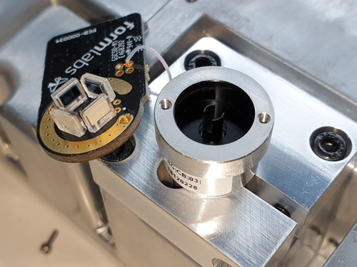
Finally, we arrive at the optics engine of the LPU. Removing the outer cover reveals a handsome optics package. The parabolic mirror is centrally prominent; immediately above it is the heat-sinked laser. Beneath the parabolic mirror is the galvanometer. Light fires from the laser, into the galvanometer, reflecting off a flat mirror (looks like a clear piece of glass, but presumably coated to optimally reflect the near-UV laser wavelength) down onto the parabolic mirror, and from there out the exit aperture to the resin tank. The white patch in the mid-left is a “getter” that helps maintain the environment within the environmentally sealed optical unit should any small amounts of contaminant make their way in.

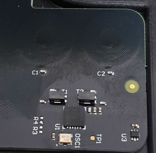
There’s an incredibly subtle detail in the LPU that really made me do a double-take. There is a PCB inside that is the “Laser Scattering Detector” assembly. It contains six photodiodes that are used in conjunction with the calibration standard to provide feedback on the laser. The PCB isn’t flat – it’s ever so slightly curved. I’ve provided a shot of the PCB in the above photo, and highlighted the area to look for on the right hand side, so you can compare it to that on the left. If you look carefully, the board actually bends slightly toward the viewer in this image.

I scratched my head on this a bit – getting a PCB to bend at such an accurate curvature isn’t something that can be done in the PCB manufacturing process easily. It turns out the trick is that the mounting bosses for the PCB are slightly canted, so that once screwed into the bosses the PCB takes the shape of the desired curve. This is a pretty clever trick! Which lead me to wonder why they went through such trouble to curve the PCB. The sensors themselves are pretty large-area; I don’t think the curvature was added to increase the efficiency of light collection. My best guess is that because the laser beam fires perpendicularly onto the calibration standard, the scattered light would come straight back onto the photodetectors, which themselves are perpendicular to the beam, and thus may reflect light back onto the calibration standard. Bending the PCB at a slight angle would mean that any residual light reflected off of the dector assembly would be reflected into the aluminum body of the LPU, thus reducing the self-reflection signal of the detector assembly.

Above is a detail shot showing the galvanometer, laser, and parabolic mirror assembly, with the scattering light detector PCB removed so that all these components are clearly in view.

Finally, we get to the galvanometer. The galvo retains many of the features of the Form 2’s – the quadrature-based sensing and notched shaft. The most obvious improvements are a much smaller light source, perhaps to better approximate a “point” light source, with less interference from a surrounding LED housing, and the incorporation of some amplification electronics on the PCB, presumably to reduce the effect of noise pick-up as the cables snake their way around the system.

Epilogue

Well, that’s it for the Form 3 teardown – from the exterior shell down to the lone galvanometer. I’ve had the privilege of court-side seats to observe the growth of Formlabs. There’s a saying along the lines of “the last 20% takes 80% of the effort”. Based on what I’ve seen of the Form series, that should be amended to “the last 20% takes 80% of the effort – and then you get to start on the product you meant to make in the first place”. It dovetails nicely into the observation that products don’t hit their stride until the third version (remember Windows 3.x?). From three grad students fresh out of the MIT Media Lab to a billion-dollar company, Formlabs and the Form series of printers have come a long way. I’d count myself as one of the bigger skeptics of 3D printing as a mass-production technology, but I hadn’t considered an approach like the LPU. I feel like the LPU embodies an audacious vision of the future of 3D printing that was not obvious to me as an observer about nine years ago. I’m excited to see where this all goes from here!

Can We Build Trustable Hardware?

Friday, December 27th, 2019

Why Open Hardware on Its Own Doesn’t Solve the Trust Problem

A few years ago, Sean ‘xobs’ Cross and I built an open-source laptop, Novena, from the circuit boards up, and shared our designs with the world. I’m a strong proponent of open hardware, because sharing knowledge is sharing power. One thing we didn’t anticipate was how much the press wanted to frame our open hardware adventure as a more trustable computer. If anything, the process of building Novena made me acutely aware of how little we could trust anything. As we vetted each part for openness and documentation, it became clear that you can’t boot any modern computer without several closed-source firmware blobs running between power-on and the first instruction of your code. Critics on the Internet suggested we should have built our own CPU and SSD if we really wanted to make something we could trust.

I chewed on that suggestion quite a bit. I used to be in the chip business, so the idea of building an open-source SoC from the ground-up wasn’t so crazy. However, the more I thought about it, the more I realized that this, too was short-sighted. In the process of making chips, I’ve also edited masks for chips; chips are surprisingly malleable, even post tape-out. I’ve also spent a decade wrangling supply chains, dealing with fakes, shoddy workmanship, undisclosed part substitutions – there are so many opportunities and motivations to swap out “good” chips for “bad” ones. Even if a factory could push out a perfectly vetted computer, you’ve got couriers, customs officials, and warehouse workers who can tamper the machine before it reaches the user. Finally, with today’s highly integrated e-commerce systems, injecting malicious hardware into the supply chain can be as easy as buying a product, tampering with it, packaging it into its original box and returning it to the seller so that it can be passed on to an unsuspecting victim.

If you want to learn more about tampering with hardware, check out my presentation at Bluehat.il 2019.

Based on these experiences, I’ve concluded that open hardware is precisely as trustworthy as closed hardware. Which is to say, I have no inherent reason to trust either at all. While open hardware has the opportunity to empower users to innovate and embody a more correct and transparent design intent than closed hardware, at the end of the day any hardware of sufficient complexity is not practical to verify, whether open or closed. Even if we published the complete mask set for a modern billion-transistor CPU, this “source code” is meaningless without a practical method to verify an equivalence between the mask set and the chip in your possession down to a near-atomic level without simultaneously destroying the CPU.

So why, then, is it that we feel we can trust open source software more than closed source software? After all, the Linux kernel is pushing over 25 million lines of code, and its list of contributors include corporations not typically associated with words like “privacy” or “trust”.

The key, it turns out, is that software has a mechanism for the near-perfect transfer of trust, allowing users to delegate the hard task of auditing programs to experts, and having that effort be translated to the user’s own copy of the program with mathematical precision. Thanks to this, we don’t have to worry about the “supply chain” for our programs; we don’t have to trust the cloud to trust our software.

Software developers manage source code using tools such as Git (above, cloud on left), which use Merkle trees to track changes. These hash trees link code to their development history, making it difficult to surreptitiously insert malicious code after it has been reviewed. Builds are then hashed and signed (above, key in the middle-top), and projects that support reproducible builds enable any third-party auditor to download, build, and confirm (above, green check marks) that the program a user is downloading matches the intent of the developers.

There’s a lot going on in the previous paragraph, but the key take-away is that the trust transfer mechanism in software relies on a thing called a “hash”. If you already know what a hash is, you can skip the next paragraph; otherwise read on.

A hash turns an arbitrarily large file into a much shorter set of symbols: for example, the file on the left is turned into “🐱🐭🐼🐻” (cat-mouse-panda-bear). These symbols have two important properties: even the tiniest change in the original file leads to an enormous change in the shorter set of symbols; and knowledge of the shorter set of symbols tells you virtually nothing about the original file. It’s the first property that really matters for the transfer of trust: basically, a hash is a quick and reliable way to identify small changes in large sets of data. As an example, the file on the right has one digit changed — can you find it? — but the hash has dramatically changed into “🍑🐍🍕🍪” (peach-snake-pizza-cookie).

Because computer source code is also just a string of 1’s and 0’s, we can also use hash functions on computer source code, too. This allows us to quickly spot changes in code bases. When multiple developers work together, every contribution gets hashed with the previous contribution’s hashes, creating a tree of hashes. Any attempt to rewrite a contribution after it’s been committed to the tree is going to change the hash of everything from that point forward.

This is why we don’t have to review every one of the 25+ million lines of source inside the Linux kernel individually – we can trust a team of experts to review the code and sleep well knowing that their knowledge and expertise can be transferred into the exact copy of the program running on our very own computers, thanks to the power of hashing.

Because hashes are easy to compute, programs can be verified right before they are run. This is known as closing the “Time-of-Check vs Time-of-Use” (TOCTOU) gap. The smaller the gap between when the program is checked versus when it is run, the less opportunity there is for malicious actors to tamper with the code.

Now consider the analogous picture for open source in the context of hardware, shown above. If it looks complicated, that’s because it is: there are a lot of hands that touch your hardware before it gets to you!

Git can ensure that the original design files haven’t been tampered with, and openness can help ensure that a “best effort” has been made to build and test a device that is trustworthy. However, there are still numerous actors in the supply chain that can tamper with the hardware, and there is no “hardware hash function” that enables us to draw an equivalence between the intent of the developer, and the exact instance of hardware in any user’s possession. The best we can do to check a modern silicon chip is to destructively digest and delayer it for inspection in a SEM, or employ a building-sized microscope to perform ptychographic imaging.

It’s like the Heisenberg Uncertainty Principle, but for hardware: you can’t simultaneously be sure of a computer’s construction without disturbing its function. In other words, for hardware the time of check is decoupled from the time of use, creating opportunities for tampering by malicious actors.

Of course, we entirely rely upon hardware to faithfully compute the hashes and signatures necessary for the perfect trust transfer of trust in software. Tamper with the hardware, and all of a sudden all these clever maths are for naught: a malicious piece of hardware could forge the results of a hash computation, thus allowing bad code to appear identical to good code.

Three Principles for Building Trustable Hardware

So where does this leave us? Do we throw up our hands in despair? Is there any solution to the hardware verification problem?

I’ve pondered this problem for many years, and distilled my thoughts into three core principles:

1. Complexity is the enemy of verification. Without tools like hashes, Merkel trees and digital signatures to transfer trust between developers and users, we are left in a situation where we are reduced to relying on our own two eyes to assess the correct construction of our hardware. Using tools and apps to automate verification merely shifts the trust problem, as one can only trust the result of a verification tool if the tool itself can be verified. Thus, there is an exponential spiral in the cost and difficulty to verify a piece of hardware the further we drift from relying on our innate human senses. Ideally, the hardware is either trivially verifiable by a non-technical user, or with the technical help of a “trustable” acquaintance, e.g. someone within two degrees of separation in the social network.

2. Verify entire systems, not just components. Verifying the CPU does little good when the keyboard and display contain backdoors. Thus, our perimeter of verification must extend from the point of user interface all the way down to the silicon that carries out the secret computations. While open source secure chip efforts such as Keystone and OpenTitan are laudable and valuable elements of a trustable hardware ecosystem, they are ultimately insufficient by themselves for protecting a user’s private matters.

3. Empower end-users to verify and seal their hardware. Delegating verification and key generation to a central authority leaves users exposed to a wide range of supply chain attacks. Therefore, end users require sufficient documentation to verify that their hardware is correctly constructed. Once verified and provisioned with keys, the hardware also needs to be sealed, so that users do not need to conduct an exhaustive re-verification every time the device happens to leave their immediate person. In general, the better the seal, the longer the device may be left unattended without risk of secret material being physically extracted.

Unfortunately, the first and second principles conspire against everything we have come to expect of electronics and computers today. Since their inception, computer makers have been in an arms race to pack more features and more complexity into ever smaller packages. As a result, it is practically impossible to verify modern hardware, whether open or closed source. Instead, if trustworthiness is the top priority, one must pick a limited set of functions, and design the minimum viable verifiable product around that.

The Simplicity of Betrusted

In order to ground the conversation in something concrete, we (Sean ‘xobs’ Cross, Tom Mable, and I) have started a project called “Betrusted” that aims to translate these principles into a practically verifiable, and thus trustable, device. In line with the first principle, we simplify the device by limiting its function to secure text and voice chat, second-factor authentication, and the storage of digital currency.

This means Betrusted can’t browse the web; it has no “app store”; it won’t hail rides for you; and it can’t help you navigate a city. However, it will be able to keep your private conversations private, give you a solid second factor for authentication, and perhaps provide a safe spot to store digital currency.

In line with the second principle, we have curated a set of peripherals for Betrusted that extend the perimeter of trust to the user’s eyes and fingertips. This sets Betrusted apart from open source chip-only secure enclave projects.

Verifiable I/O

For example, the input surface for Betrusted is a physical keyboard. Physical keyboards have the benefit of being made of nothing but switches and wires, and are thus trivial to verify.

Betrusted’s keyboard is designed to be pulled out and inspected by simply holding it up to a light, and we support different languages by allowing users to change out the keyboard membrane.

The output surface for Betrusted is a black and white LCD with a high pixel density of 200ppi, approaching the performance of ePaper or print media, and is likely sufficient for most text chat, authentication, and banking applications. This display’s on-glass circuits are entirely constructed of transistors large enough to be 100% inspected using a bright light and a USB microscope. Below is an example of what one region of the display looks like through such a microscope at 50x magnification.

The meta-point about the simplicity of this display’s construction is that there are few places to hide effective back doors. This display is more trustable not just because we can observe every transistor; more importantly, we probably don’t have to, as there just aren’t enough transistors available to mount an attack.

Contrast this to the more sophisticated color displays, which rely on a fleck of silicon with millions of transistors implementing a frame buffer and command interface, and this controller chip is closed-source. Even if such a chip were open, verification would require a destructive method involving delayering and a SEM. Thus, the inspectability and simplicity of the LCD used in Betrusted is fairly unique in the world of displays.

Verifiable CPU

The CPU is, of course, the most problematic piece. I’ve put some thought into methods for the non-destructive inspection of chips. While it may be possible, I estimate it would cost tens of millions of dollars and a couple years to execute a proof of concept system. Unfortunately, funding such an effort would entail chasing venture capital, which would probably lead to a solution that’s closed-source. While this may be an opportunity to get rich selling services and licensing patented technology to governments and corporations, I am concerned that it may not effectively empower everyday people.

The TL;DR is that the near-term compromise solution is to use an FPGA. We rely on logic placement randomization to mitigate the threat of fixed silicon backdoors, and we rely on bitstream introspection to facilitate trust transfer from designers to user. If you don’t care about the technical details, skip to the next section.

The FPGA we plan to use for Betrusted’s CPU is the Spartan-7 FPGA from Xilinx’s “7-Series”, because its -1L model bests the Lattice ECP5 FPGA by a factor of 2-4x in power consumption. This is the difference between an “all-day” battery life for the Betrusted device, versus a “dead by noon” scenario. The downside of this approach is that the Spartan-7 FPGA is a closed source piece of silicon that currently relies on a proprietary compiler. However, there have been some compelling developments that help mitigate the threat of malicious implants or modifications within the silicon or FPGA toolchain. These are:

• The Symbiflow project is developing a F/OSS toolchain for 7-Series FPGA development, which may eventually eliminate any dependence upon opaque vendor toolchains to compile code for the devices.
Prjxray is documenting the bitstream format for 7-Series FPGAs. The results of this work-in-progress indicate that even if we can’t understand exactly what every bit does, we can at least detect novel features being activated. That is, the activation of a previously undisclosed back door or feature of the FPGA would not go unnoticed.
• The placement of logic with an FPGA can be trivially randomized by incorporating a random seed in the source code. This means it is not practically useful for an adversary to backdoor a few logic cells within an FPGA. A broadly effective silicon-level attack on an FPGA would lead to gross size changes in the silicon die that can be readily quantified non-destructively through X-rays. The efficacy of this mitigation is analogous to ASLR: it’s not bulletproof, but it’s cheap to execute with a significant payout in complicating potential attacks.

The ability to inspect compiled bitstreams in particular brings the CPU problem back to a software-like situation, where we can effectively transfer elements of trust from designers to the hardware level using mathematical tools. Thus, while detailed verification of an FPGA’s construction at the transistor-level is impractical (but still probably easier than a general-purpose CPU due to its regular structure), the combination of the FPGA’s non-determinism in logic and routing placement, new tools that will enable bitstream inspection, and the prospect of 100% F/OSS solutions to compile designs significantly raises the bar for trust transfer and verification of an FPGA-based CPU.


Above: a highlighted signal within an FPGA design tool, illustrating the notion that design intent can be correlated to hardware blocks within an FPGA.

One may argue that in fact, FPGAs may be the gold standard for verifiable and trustworthy hardware until a viable non-destructive method is developed for the verification of custom silicon. After all, even if the mask-level design for a chip is open sourced, how is one to divine that the chip in their possession faithfully implements every design feature?

The system described so far touches upon the first principle of simplicity, and the second principle of UI-to-silicon verification. It turns out that the 7-Series FPGA may also be able to meet the third principle, user-sealing of devices after inspection and acceptance.

Sealing Secrets within Betrusted

Transparency is great for verification, but users also need to be able to seal the hardware to protect their secrets. In an ideal work flow, users would:

1. Receive a Betrusted device

2. Confirm its correct construction through a combination of visual inspection and FPGA bitstream randomization and introspection, and

3. Provision their Betrusted device with secret keys and seal it.

Ideally, the keys are generated entirely within the Betrusted device itself, and once sealed it should be “difficult” for an adversary with direct physical possession of the device to extract or tamper with these keys.

We believe key generation and self-sealing should be achievable with a 7-series Xilinx device. This is made possible in part by leveraging the bitstream encryption features built into the FPGA hardware by Xilinx. At the time of writing, we are fairly close to understanding enough of the encryption formats and fuse burning mechanisms to provide a fully self-hosted, F/OSS solution for key generation and sealing.

As for how good the seal is, the answer is a bit technical. The TL;DR is that it should not be possible for someone to borrow a Betrusted device for a few hours and extract the keys, and any attempt to do so should leave the hardware permanently altered in obvious ways. The more nuanced answer is that the 7-series devices from Xilinx are quite popular, and have received extensive scrutiny over its lifetime by the broader security community. The best known attacks against the 256-bit CBC AES + SHA-256 HMAC used in these devices leverages hardware side channels to leak information between AES rounds. This attack requires unfettered access to the hardware and about 24 hours to collect data from 1.6 million chosen ciphertexts. While improvement is desirable, keep in mind that a decap-and-image operation to extract keys via physical inspection using a FIB takes around the same amount of time to execute. In other words, the absolute limit on how much one can protect secrets within hardware is probably driven more by physical tamper resistance measures than strictly cryptographic measures.

Furthermore, now that the principle of the side-channel attack has been disclosed, we can apply simple mitigations to frustrate this attack, such as gluing shut or removing the external configuration and debug interfaces necessary to present chosen ciphertexts to the FPGA. Users can also opt to use volatile SRAM-based encryption keys, which are immediately lost upon interruption of battery power, making attempts to remove the FPGA or modify the circuit board significantly riskier. This of course comes at the expense of accidental loss of the key should backup power be interrupted.

At the very least, with a 7-series device, a user will be well-aware that their device has been physically compromised, which is a good start; and in a limiting sense, all you can ever hope for from a tamper-protection standpoint.

You can learn more about the Betrusted project at our github page, https://betrusted.io. We think of Betrusted as more of a “hardware/software distro”, rather than as a product per se. We expect that it will be forked to fit the various specific needs and user scenarios of our diverse digital ecosystem. Whether or not we make completed Betrusted reference devices for sale will depend upon the feedback of the community; we’ve received widely varying opinions on the real demand for a device like this.

Trusting Betrusted vs Using Betrusted

I personally regard Betrusted as more of an evolution toward — rather than an end to — the quest for verifiable, trustworthy hardware. I’ve struggled for years to distill the reasons why openness is insufficient to solve trust problems in hardware into a succinct set of principles. I’m also sure these principles will continue to evolve as we develop a better and more sophisticated understanding of the use cases, their threat models, and the tools available to address them.

My personal motivation for Betrusted was to have private conversations with my non-technical friends. So, another huge hurdle in all of this will of course be user acceptance: would you ever care enough to take the time to verify your hardware? Verifying hardware takes effort, iPhones are just so convenient, Apple has a pretty compelling privacy pitch…and “anyways, good people like me have nothing to hide…right?” Perhaps our quixotic attempt to build a truly verifiable, trustworthy communications device may be received by everyday users as nothing more than a quirky curio.

Even so, I hope that by at least starting the conversation about the problem and spelling it out in concrete terms, we’re laying the framework for others to move the goal posts toward a safer, more private, and more trustworthy digital future.

The Betrusted team would like to extend a special thanks to the NLnet foundation for sponsoring our efforts.