The ware for March 2011 is shown below. Click on the image for a much larger version.

Despite the cropping and sanitizing of this image, I suspect this will still be guessed very quickly…
This entry was posted on Sunday, April 3rd, 2011 at 4:58 am and is filed under Hacking. You can follow any responses to this entry through the RSS 2.0 feed.
Both comments and pings are currently closed.
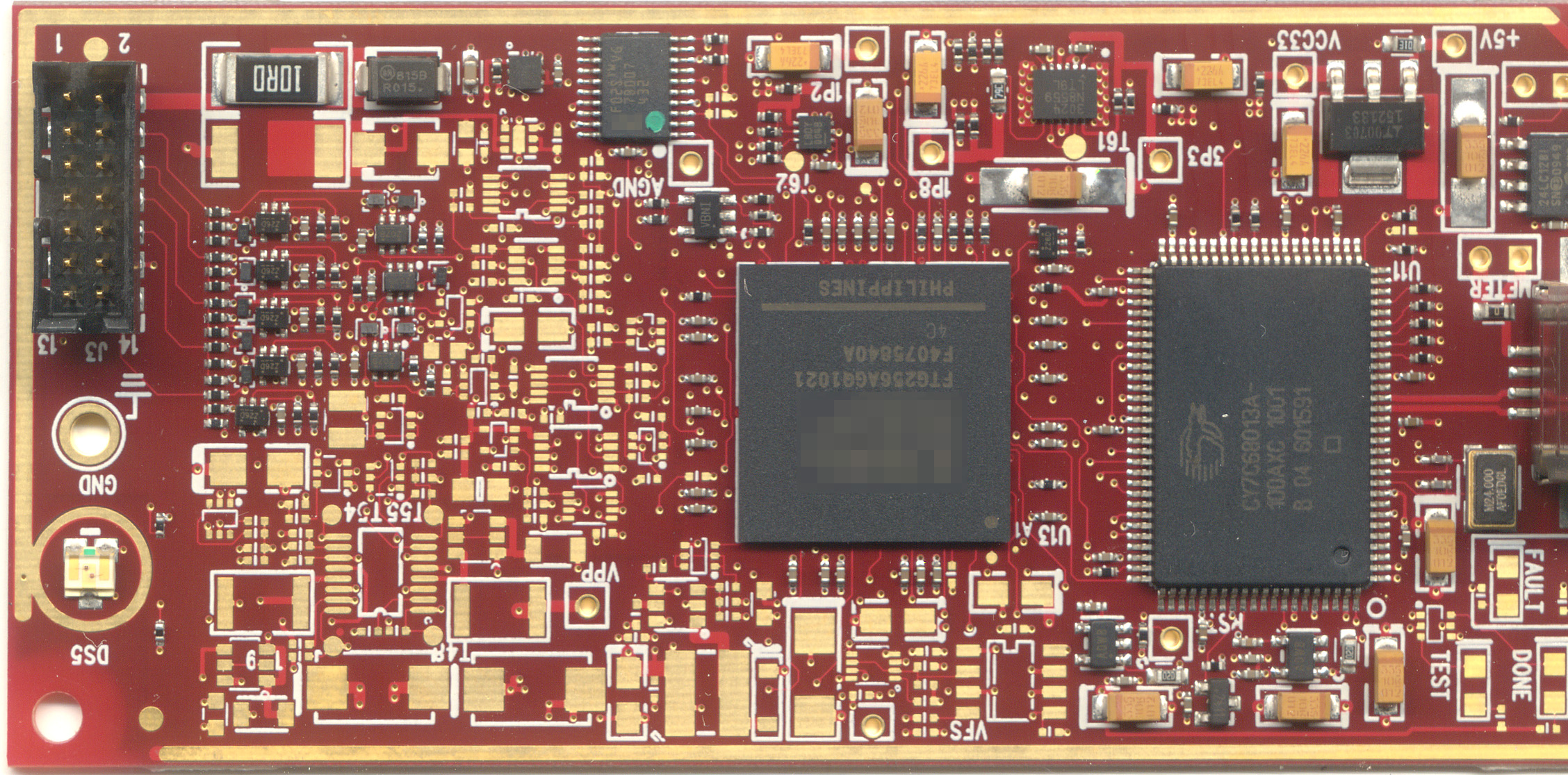
The ‘4C’ at the bottom of the BGA chip looks like it might be an FPGA speed marking, and the chip on the right is a USB transceiver according to the part marking (associated with a just-out-of-shot USB port on the far right).
I think it’s some sort of USB-based FPGA development board. A wild guess would be an older Opal Kelly one, based on your recommendation of them.
The BGA package in the centre is an Xilnix FPGA and the other large package is a Cypress USB controller.
My guess is that it’s a USB JTAG adapter.
To further that guess, the only external IO appears to be a USB type connector and what seems to be a JTAG header.
There seems to be some sort of level-shifting or protection for the 5 signal lines connected to the 7×2 connector, which would make sense for a JTAG adapter.
There is quite a large number of un-populated pads which is curious, possibly this is a base model device? The large 10R resistor also stands out as interesting.
That first big chip looks like an FPGA or CPLD (FTG256 is a Xilinx package designation, I believe), the other one is a Cypress USB controller chip (EZ-USB FX2LP). It looks familiar, but I just can’t place it.
Assuming I’ve read the datasheet right, the FTG256 package is 15x15mm, so the board looks around 4cm wide. If I had to guess, might it be a Xilinx Platform Cable USB board?
yes, indeed – i’ve not been able to find any schematics of such cable, but physical aspect and pinout match with some “Xilinx PUSB latform Cable II”, and according to XUP’s programmers (http://inisyn.org/src/xup/), that programmer architecture would match with what xilinx uses usually.
The 14 pin connector, looking like arm JTAG iface, it’s array of buffers, the cypress EZ-USB FX2 USB chip, and the Xilinx (spartan-3a?) package at the center makes me think about some sort of regular high speed JTAG emulator design.
The non populated printouts and the pcb look makes think of some commercial product, available in a couple of different version. but a first look at the pinout of the connector does not really match with standard JTAG connector… so it could basically be any kind of chip programmer / emulator…
BUT – after a quick scan of various vendor jtag pinouts, it could simply be a xilinx one, (http://www.jtagtest.com/pinouts/xilinx), so, let’s guess it’s a jtag programmer for xilinx chips..
It’s a DS300 Platform Cable USB by Xilinx
Datasheet here: http://xilinx.com/support/documentation/data_sheets/ds300.pdf
Full image here: http://www.mikrocontroller.net/attachment/55837/DLC10.jpg
Judging by the form-factor, Cypress chip, Xilinx Spartan FPGA, and the location of the header and LED, I’d say this is a Xilinx Platform Cable I or II.
I second PiX, it’s the platform USB II pod from Xilinx. I recognized the red PCB. The chip with the green dot is an XCF02 Platform Flash chip to configure the Xilinx FPGA. The Cypress MCU and USB connector give away the USB connectivity. There’s a lot more protection on the JTAG I/O than would be normal on a programming port for a typical FPGA design. The dual-color LED in the right location also gives away the fact that it’s a Xilinx cable. Of course, the link PiX posted pretty much nails it.
But seriously, I wonder what’s with all those unpopulated components…
It’s nicely made, with gold-flashed pads, and designed for manufacturability: some of the capacitor pads are long, to accomodate different size components, allowing substitution. Looks like one of the Cypress USB capable CPUs, with nice wide traces to the data leads. I’m amused by the 0-ohm resistor across the “meter” contacts. I guess that’s to measure current draw in some variant. There are several power buses, and a reference to “AGND”, which implies that it may not be a fully digital design. I suspect the 10-ohm resistor and associated wide trace is for current draw measurement, which would work with an analog section. The drivers for the Berg connector imply it’s driving something, and needs extra oomph, protection, or both. I’m guessing some sort of ISP device designed to check for various board faults and report back on them. Obviously a base model, with lots of optional circuitry unpopulated.
Having opened one of these less than a week ago, I recognized it instantly. As others have stated, it is a Platform Cable USB II from Xilinx. I wish I would have logged in Sunday.
Also, for those wondering about unpopulated components, there are schematics downloadable from xilinx.com.
I’ve never opened mine up, but yeah, given the placement of the header and LED I knew what it was almost immediately.
As several people mentioned, it’s curious that there are so many unpopulated components. I wonder what kind of features are enabled when the missing components are placed.
Xilinx “Platform Cable USB II”
Model: DLC10 / Part No.: HW-USB-II-G
http://www.xilinx.com/products/devkits/HW-USB-II-G.htm
(apparently this is exactly the product shown in the image posted by PiX: http://www.mikrocontroller.net/attachment/55837/DLC10.jpg and appears an exact match to the Ware.)
So the question is: if there is only one version of the DLC10 available, why are 60% of the components absent?