Akiba is providing a running commentary of the MIT Media Lab IAP China immersion experience. If you’re curious about it, check it out. So far he has day 1 and day 2 up.
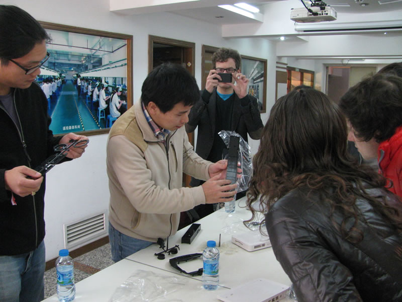
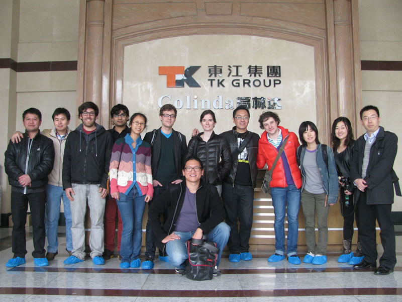
Above is a photo of Colman Lee, a mechanical designer from AQS, lecturing the students about some of the more subtle aspects of mold and tool design. AQS is my go-to manufacturing services partner / general problem solving crew, and they helped with many of the local arrangements for the trip. Below is a group photo at Colinda, our first stop on the tour where we got to take a look inside the Onyx Geiger counter injection molding tool.
Good read from Akiba, would love to join this trip :)
I have been into all the big and small factory in China and it never stop amazed me with how much technology they have far ahead from other country hidden in a dull looking factory. The outsourcing practice really make China the go to place for all those thing.
Which is a heaven for people who love seeing their product come together :)
As expected, very nice read accompanied by pictures saying a thousand words. Your blog and Akiba’s complement each other synergetically.
I have a question for anyone reading this blog: Where can I found a good resource for learning how to repair products with LCD connected via elastomer “zebra” strips. Those are featured in a lot of products, some of them high-end (like Fluke multimeters), but it was impossible to me to reliably repair those contacts, despite trying some tricks from the Internet like boiling the strips or rubbing them with denaturated alcohol. Would like to know how are they professionally installed on the assembly line, how are they aligned, are unused rolls of strips can be bought in small quantities anywhere ? Is there a better way to repair those contacts ?
No alignment but up/down; just have more striping than the pads have s.t. your signal does not short across pads. You can read maker spec or chat up their fabs, but they’re just striped conductors and the LCD driver is wagging 7-16V (some to make up for side resistance worst-case.) It could be graphite, it could be epitaxial tin; but the focus was on the conductor layer, so the other layers mostly don’t. Avoiding contamination or having spare is all there is to it; did boiling in DI water ever work? Saltwater and lightly cleaned edges FTW? Those elastomers could have hardened up or failed internally, so new materiel beats test beyond segment contact (usually better than naked SnO(x) (which slooowly oxidizes) so no use cleaning the display contacts beyond particulates most times.
Hey, where’s the obsessive onshoring meme with Akiba? Isn’t the dream to be dating a maid-cafe girl who has multiple PhDs in rocket science and an obsessively brought-to-compliance Traditional Japanese Multichip Packaging Fab from the 1300s? (Nobunaga the CMP licensee…surely you heard.)
[…] Updates from the Tour in China (Bunnie Huang) — my dream geek tourism trip: going around Chinese factories and bazaars with MIT geeks. […]
[…] written a brief summary of his activities so far on his manufacturing tour of China with the MIT Media Lab. Our mutual friend Akiba, who’s also along on the trip, has some nice […]
You are assuming that manufacturing has to be done in China. How about asking the question of what is most cost effective. For a counter perspective check out the article The Insourcing Boom by Charles Fishman. It discusses how GE is moving appliance mfg back to US and is saving money.
http://www.theatlantic.com/magazine/archive/2012/12/the-insourcing-boom/309166/
You’re assuming that’s my assumption. The lessons learned by the students can be applied anywhere in the world. In fact, after they are done here, they are expected to take their learning back to Cambridge and apply it to their research.
The course is in China because Shenzhen just happens to be one of the few places in the world where you can tour hundreds of world-class factory facilities within a one-hour car ride from the city center, and it also has the largest electronics component market to boot. It would be very hard and expensive to teach a class with so much hands-on access anywhere else.
B,
Great articles, the Shenzhen tour looks awesome. I want to go next time! I really like how you tackled the BOM and DFM aspects of manufacturing in China.
Andrew
Good info. Lucky me I discovered your site by chance (stumbleupon). I’ve saved as a favorite for later!