In January, I had the fortune of being a keynote speaker at LCA2013. One of the tchotchkes I received from the conference organizers was a little USB memory stick.
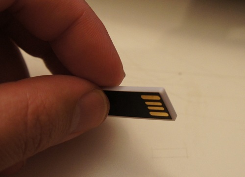

I thought it was a neat coincidence that I was in a factory that manufactured exactly such memory sticks about a week before the conference. In fact, I managed to score a rare treat: the factory owner gave me a sheet of raw chip-on-flex, prior to bonding and encapsulation, to take home.
The USB sticks start life as bare FLASH memory chips. Prior to mounting on PCBs, the chips are screened for capacity and functionality. Below is a photo of the workstation where this happens:
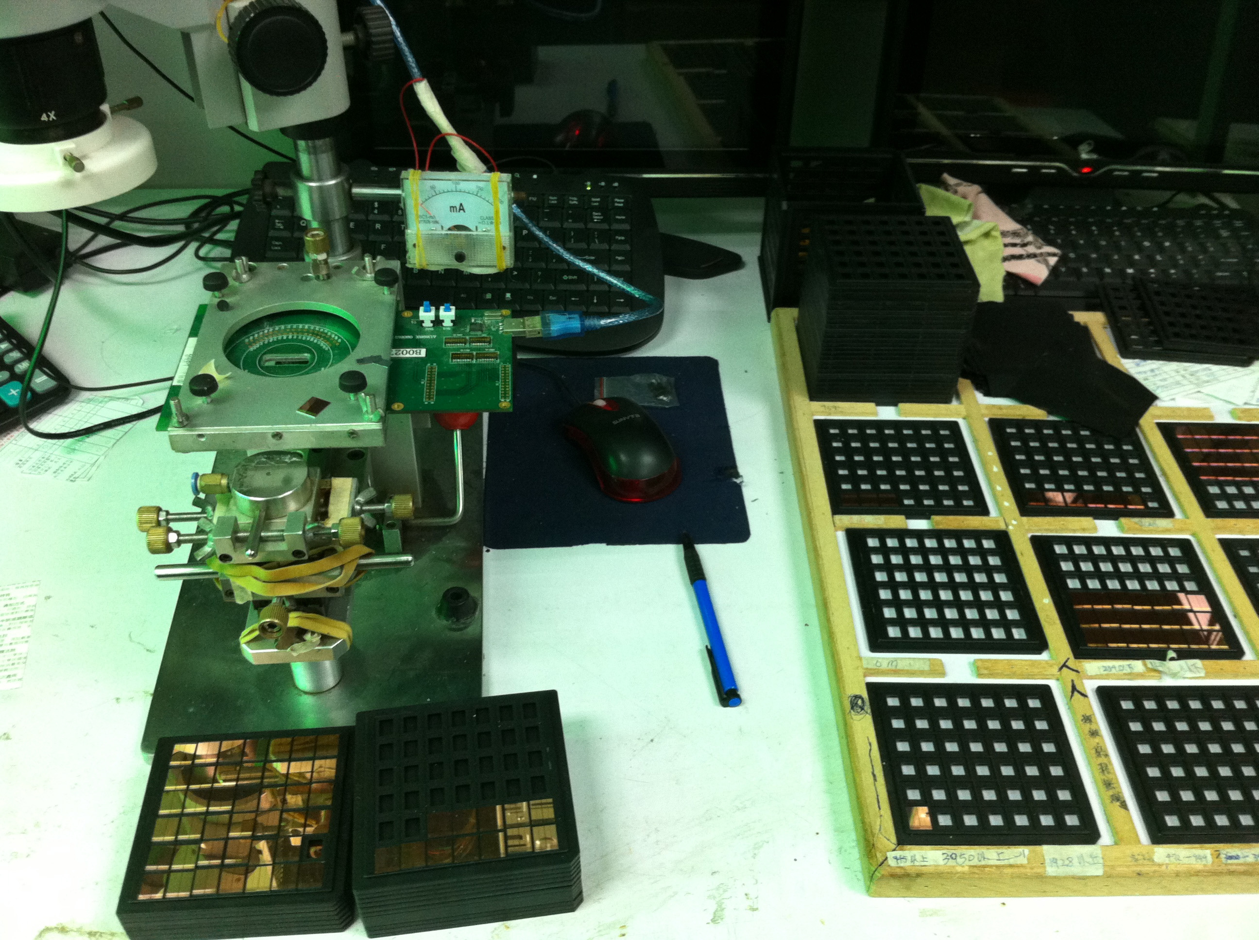
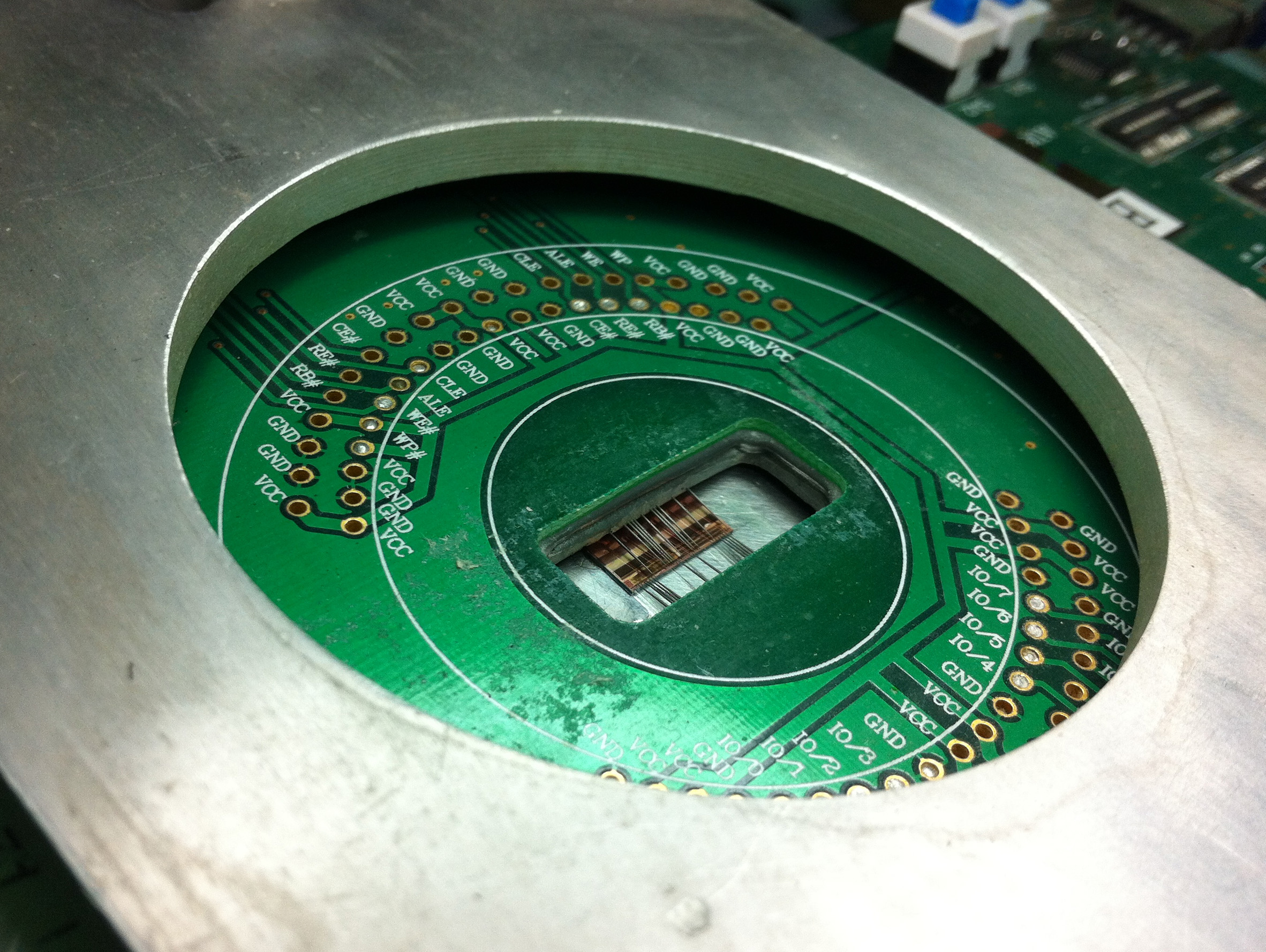
In the image, you can see stacks of bare-die FLASH chips, awaiting screening with a probe card. I love the analog current meter and the use of rubber bands to hold it all together. The probe card has tiny needles on it that touch down on microscopic (less than 100-micron square) contacts on the chip surfaces. Below is what a probe card looks like.
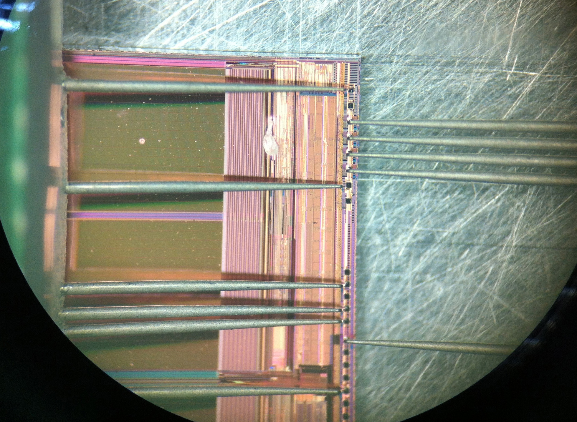
Below is an image through the microscope on the micro-probing station, showing the needles touching down on the square pads at the edge of the FLASH chip’s surface.
Interestingly, this all happens in an absolutely non-clean-room environment. Workers are pretty much handling chips with tweezers and hand suction vises, and mounting the devices into these jigs by hand.
Once the chips are screened for functionality, they are placed by hand onto a PCB. This is not an unusual practice, pretty much every value-oriented wirebonding facility I’ve visited relies on the manual placement of bare die. The photo below shows a controller IC being placed on a panel of PCBs. The bare die are in the right hand side of the photo, sitting in the beige colored waffle pack.

The lady is using some sort of tool made out of hand-cut bamboo. I still haven’t figured out exactly how they work, but every time I’ve seen this process they are using what looks like a modified chopstick to place the chips on the board. My best guess is that the bamboo sticks have just the right surface energy to adhere to the silicon die, such that silicon will stick to the tip of the bamboo rod. A dot of glue is pre-applied to the bare boards, so when the operator touches the die down onto the glue, the surface tension of the glue pulls the die off of the bamboo stick.
It’s trippy to think that the chips inside my USB stick were handled using modified chopsticks.

The chips are then wirebonded to the board using an automated bonding machine which uses image recognition to find the location of the bond pads (this is part of the reason they can get away with manual die placement).
The first half of the video above starts out with the operator pulling off and replacing a mis-bonded wire by hand, and re-feeding the wire into the machine. Given that these wires are thinner than a strand of hair, and that the bonding pads are microscopic, this is no mean feat of manual dexterity.
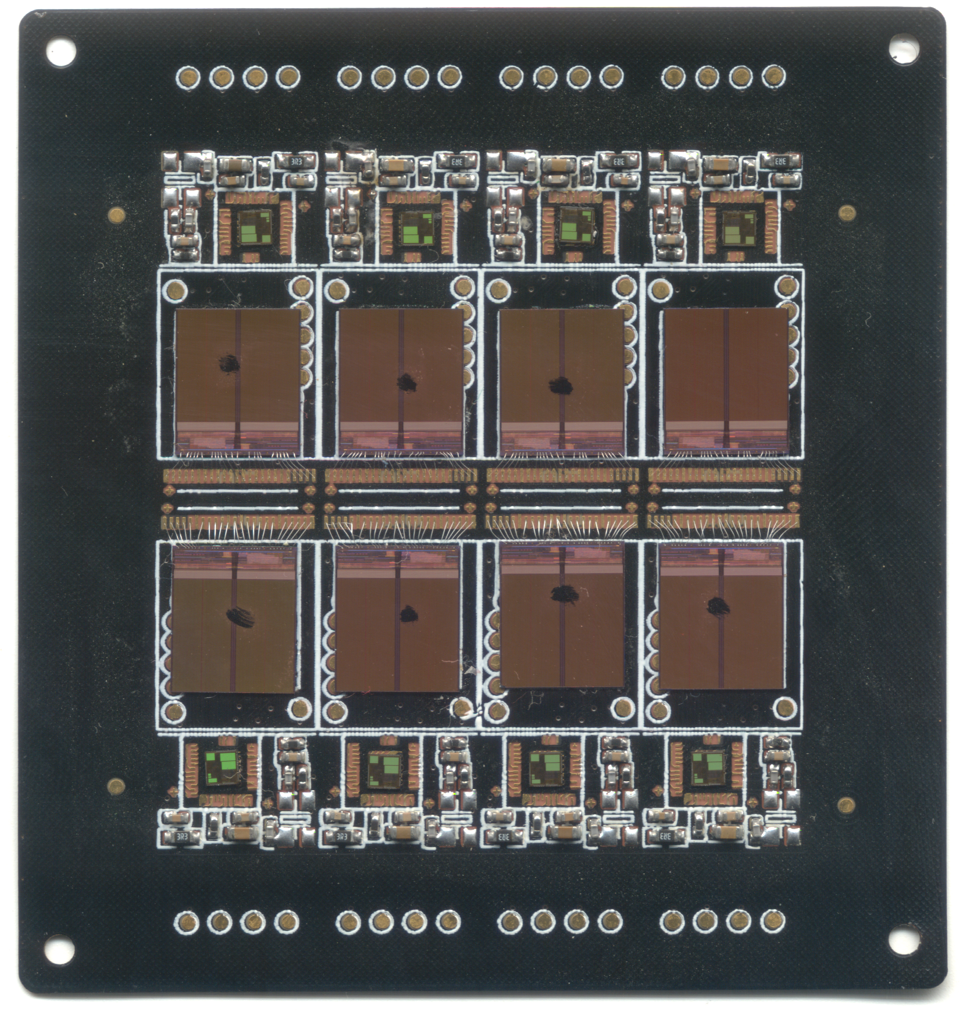
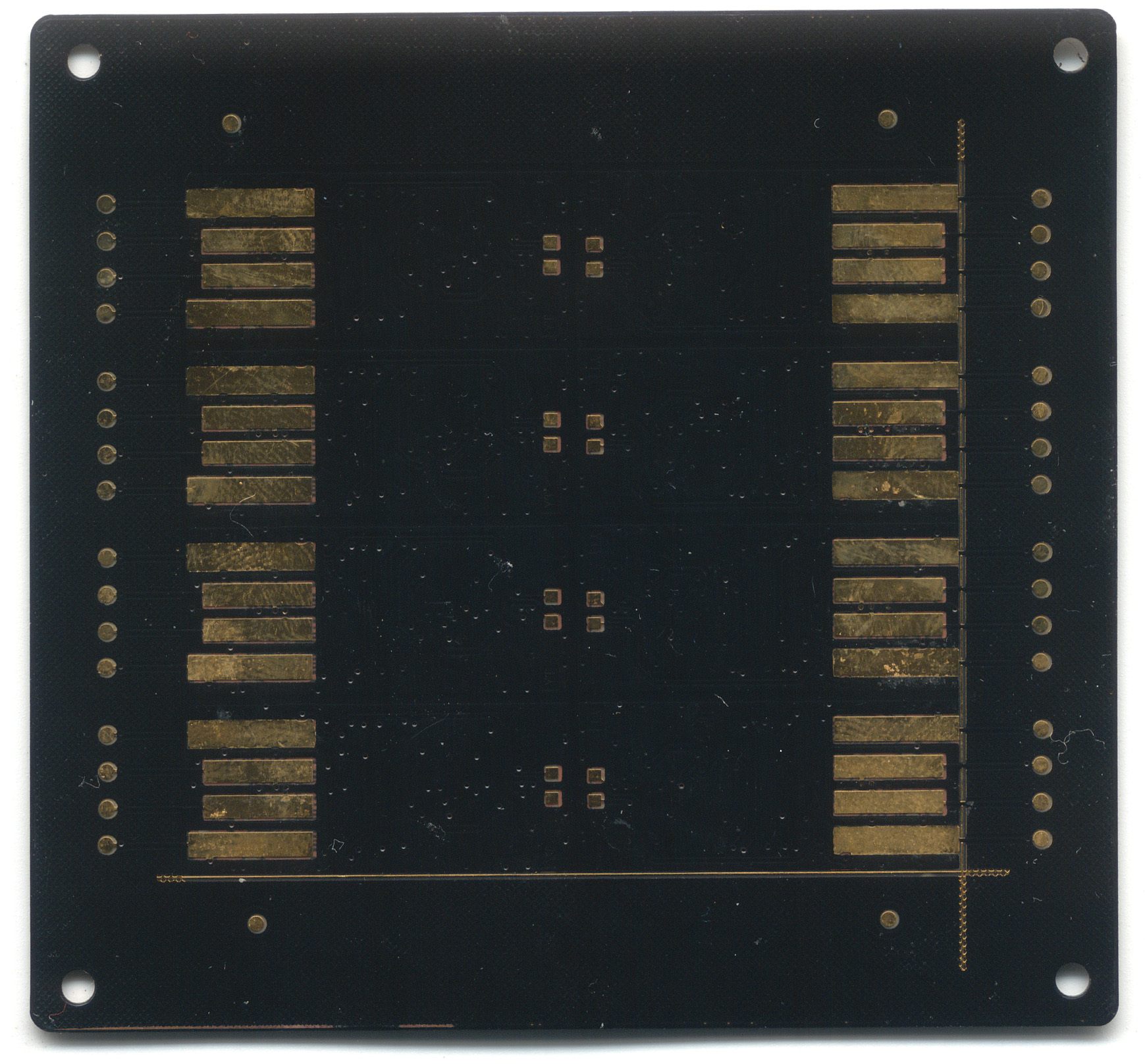
Here’s a scan of the partially-bonded but fully die-mounted PCB that I was given as a memoir from my visit (I had since crushed some of the wire bonds). The panel contains eight USB sticks, each consisting of a FLASH memory chip and a controller IC that handles the bridging between USB and raw FLASH, a non-trivial task that includes managing bad block maps and error-correction, among other things. The controller is probably an 8051-class CPU running at a few dozen MHz.
Once the panels are bonded and tested, they are overmolded with epoxy, and then cut into individual pieces, ready for sale.
Interestingly, the entire assembly prior to encapsulation is flexible. The silicon chips have been thinned down by grinding off their back sides to the point where they can tolerate a small amount of flexing, and the PCB is also so thin, it is flexible.

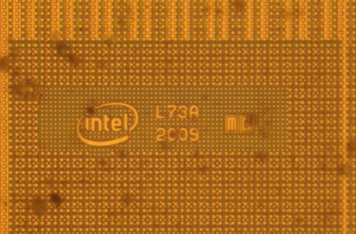
For those of you interested in this kind of thing, here’s the die marking from the FLASH chip; apparently it is made by Intel:
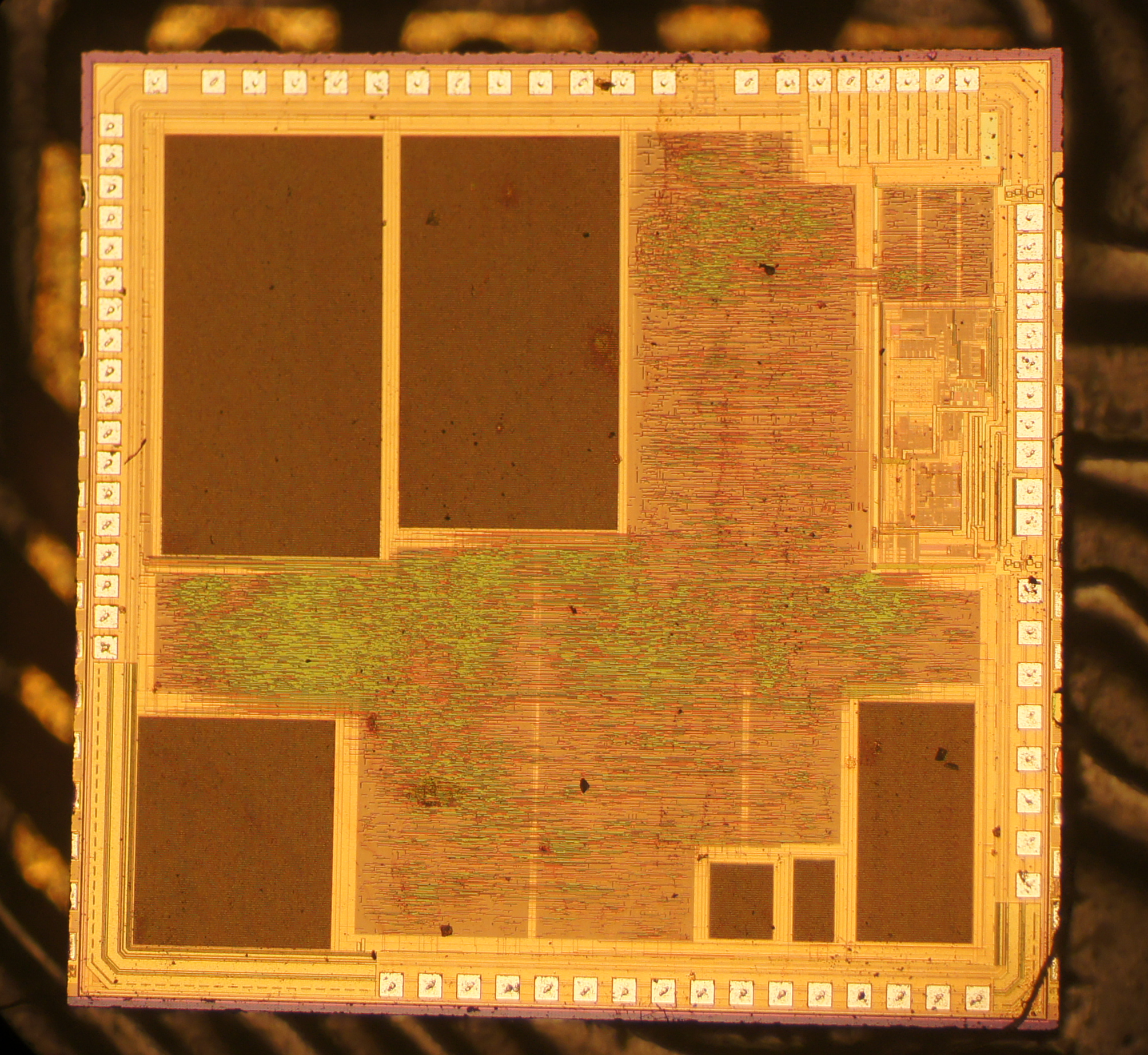
Here is also a die shot of the controller chip:
And now you know where those tiny USB thumb drives are born.
Thanks to David Cranor for contributing images. Images used with permission.
PS: chopsticks
No pics of the station where they load the spyware?
It’s in there – you just missed it.
You don’t think that the only thing they at the die testing station is test the dice? They have everything they need for programming the dice.
(I don’t seriously believe that spyware is loaded, but this could be where customer specified preloaded files would be written to the dice.)
Unless they’re ordering in major bulk, the customer-specified preloading would be easier to do on finished products. Adding on a process is easier than modifying one in this case, IMO. You can just grab the number you need from the pile of drives in the nearest bin, instead of setting up a dedicated line to programming the chips during construction.
Wow – fascinating. Magic chopsticks – who would’ve guessed?
Do you know how the needles on the test jig are set into place? This seems like an exacting job that needs to be re-done for each new chip that comes onto the line. Is there a special manufacturer for them, or does the factory fabricate them themselves?
I believe there is an entire industry that supports making probe cards (PCBs with carefully mounted probe needles). Every silicon manufacturer has to test their product, and they all need probe cards.
[…] Your USB Sticks Are Made With Chopsticks (Bunnie Huang) — behind-the-scenes on how USB sticks are made. […]
Chopstick or spudger?
http://en.wikipedia.org/wiki/Spudger
If someone put a pair of these in front of me in a Chinese restaurant I would use them to eat my food without question. :)
I use chopsticks all the time for working with small solder joints. The balsa ones are better than bamboo if you want more absorption (say, flux).
You don’t need a clean room for working with the die after it’s been manufactured. Depackaging and rebonding work fine in a normal household environment, just ask Chris Tarnovsky.
I already had some keys like that and I had a question:
what are the two 0603 sized pads at the opposite of the usb connector made for? I never had the time to solder a LED in this place :)
(they are visible in groups of 4 in usb1q13_back.jpg )
[…] Where USB Memory Sticks are Born, USB sticks are assembled in a less than high-tech environment. […]
tell me something, how much would that cost, with branding?
What surprises me is that the flash suppliers haven’t integrated a controller onto the flash die. Same for SD cards, where the controller chip is usually piggy backed onto a corner of the flash.
Is this some process issue, perhaps? Given the easy integration of flash blocks in normal logic, I would expect not, but maybe not at the extreme levels of density here. Even so, this is hardly like a DRAM process.
Given that portable storage is currently the largest consumer of medium-capacity flash dies, and it is an incredibly cost-sensitive market, surely there is a technical reason this isn’t done?
Controller need high ESD protection, USB support 5v signal but smaller process is harder to protect, more easily to damaged by high voltage.
You called it. The chip fabrication procedures for memory and CPU differ considerably. Trying to shoehorn controllers onto memory wafers dramatically decreases flawless yields. Given how cutthroat the commodity fab business is, that would quickly send the experimenter out of business.
That is not to say that someone with a large enough bankroll and a good enough fab couldn’t built a process that does it cost competitively, but it would probably take tens to hundreds of millions to build up, and would be money lost with the next drop in feature size.
Realistically, until we get to the point of widescale custom printing on an atomic scale, separate chips made with separate processes are more cost effective.
For those that are curious, a L73A die is a MLC 32Gb NAND device built on a 29nm process (probably at the IMFT facility).
hi Bunnie,
how can i contact you in private ?
I would to develop a new idea with UDP’s manufacturers and I have seen pictures of those factories in your blog.
Thanks
Alex ( from Spain )
Hi bunny, i would like to ask for some think ee in priv, can you give me your fapange or twitter? best
[…] It’s a stretch to call this one a hack, but USB thumb drives are around us constantly and we always assumed that the boards inside were machine populated (like with a pick and place machine). [Bunnie] tells us otherwise. He recently had the chance to tour a factory where USB flash drives are made. […]
[…] It’s a period to summons this digit a chop, however USB thumb forces are about us constantly furthermore we always putative that the accommodates confidential were robot populated (comparable beside a harvest besides arrange device). [Bunnie] recounts us else. He recently had the adventure to trip a workshop where USB flare compels are made. […]
Nothing special with bamboo stick. I wet them with propanol , small items stick to the tip and are released when dried or soldered/glued
I am amazed that this sort of process is still being done for these USB Flash drives.
Way back in 1985 when I was doing my uni thesis on IC design, my University would get multi-project chips made at a local foundry. To make use of the relevant part of the chip for my work, I had to manually place (using Araldite) and then wire bond bare chips onto a PCB to allow me to test and use each die.
It was difficult work in that the wire-bonding machine was an old Kulicke and Soffa wedge bonder that the Uni must have got second-hand from somewhere. Often, due to problems with the machine, I would have to do a fair bit of rework using the finest tweezers and scalpel blades I could get from RS components. Happy days!
hi Bunnie,
how can i contact you in private ?
I would to develop a new idea with UDP’s manufacturers and I have seen pictures of those factories in your blog.
Thanks
Alex ( from Spain )
[…] was reading bunnie’s recent post on the manufacturing techniaues used in USB flash-drives… bare die manipulated by hand with a […]
What a comprehensive usb flash drive article.
Have learn something useful today.
Greeting from Malaysia!!
What i do not understood is in fact how you
are now not actually much more well-favored than you may be right now.
You are so intelligent. You understand thus significantly
relating to this matter, produced me in my view believe it from a lot of numerous
angles. Its like women and men aren’t involved until it is something to do with Woman gaga! Your personal stuffs nice. All the time handle it up!
Hello Bunnie,
I need to talk to this company or similar. Can you tell me the name or the site of this manufacturer.
In advance thank you.
Pasquale