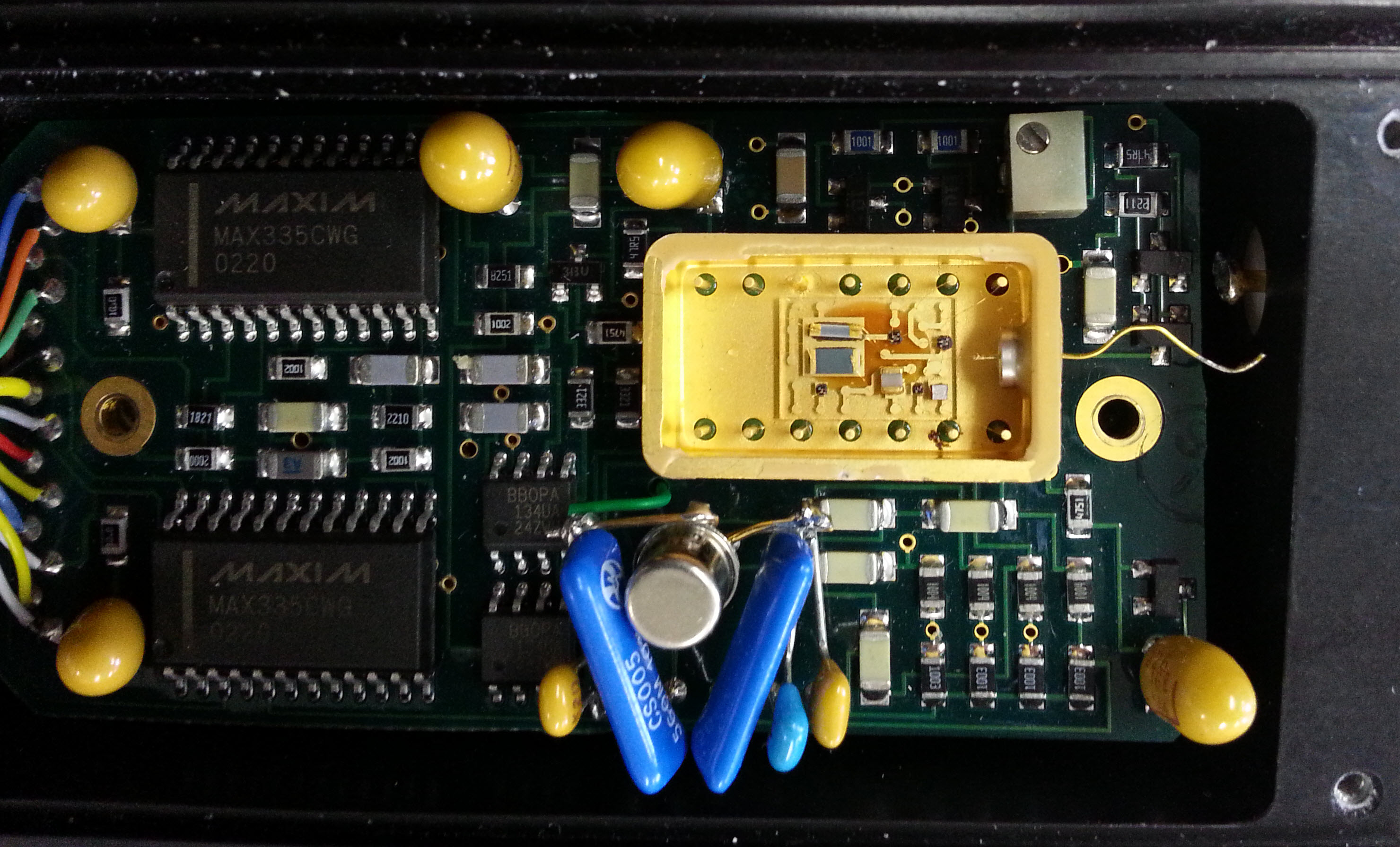
The Ware for December 2014 is shown below.

Thanks again to dmo and QB for letting me photograph this ware.
Happy holidays!
This entry was posted on Thursday, December 18th, 2014 at 4:22 pm and is filed under Hacking. You can follow any responses to this entry through the RSS 2.0 feed.
Both comments and pings are currently closed.
I’m guessing a serially controlled radio receiver.
It’s serially controlled, yes. The bottom MAX connects to the four 100k/1M resistor networks, for example.
There’s also one, maybe two precision op-amps.
I’d go with precision noise source.
The special yellow device looks like a high frequency resonator/amplifier/modulator – going likely to a bnc output for antenna/signal.
As it doesn’t seem to be any analog input (all inputs on the left look like digital inputs driving the two maxim’s), it might be a high frequency function generator, in the 1-10Ghz range (maybe even more).
From the encasing, it might be a module to a lab-sized high perf oscilloscope.
That’s not a high-frequency device. No sane RF engineer would use such non-coaxial / not-impedance-matched wire from the connector to that mystery gold-plated chip in the middle.
Perhaps something that measures very low currents? very low voltages? or measures with very high impedance (like an electrometer)?
The Maxim devices are 8 channel SPST analog 100 ohm switches, there are two OPA134 op-amps, which points to some analog application. There are 14 wires, each Maxim chip needs power, ground, clock, chip select, data in, and possible data out. These can be chained, so we only need 6-7 wires total, although if the chips are not daisy chained you would need more. I agree that the wires don’t look like they carry any precise analog or RF signals, so we’ll assume they are power and the SPI control lines to the Maxim switches. The capacitors and can (transistor?) look like they were hand reworked, which implies either a prototype or a low quantity product. The captive nuts on the surrounding case also point towards an industrial device that is meant to be serviceable.
The gold composite device in the center is the obviously expensive part, with all of the gold plating and the circuit that appears to be printed on glass, so I would guess that it is the key to the function. It has four small silicon dies and some passives, I would guess a resistor, a capacitor, a crystal, and a thermistor. I am basing these guesses off of my gut feeling that the device is a temperature controlled crystal oscillator (TCXO). This assumes that it is usually covered to keep the internal area more thermally isolated from the surroundings.
Assuming the gold device is a TCXO, what are the analog components surrounding it, and why do we need 16 independently controlled analog switches? I’m not quite sure, I assume they are intended for controlling/tuning the TCXO, but I’m not sure exactly what they would be doing. The TCXO should be internally stable, it shouldn’t need an external feedback loop, so that makes me doubt my gut feeling a bit. (Crystals also usually use two matched capacitors, which are not present in this device, unless they are external, which seems unlikely to me)
I agree with the possibility that it could be a noise source or other RF source, but also that the external connection is not ideal for very high frequencies since it is not a coax or other controlled impedance line. This implies to me that the signal is somewhat low frequency, (low GHz at the absolute max, more likely in the MHz range) This would have to apply for either a TCXO or noise/RF source. Precision pieces of test equipment often use 10MHz precision references, so this could be such a source, but that again leaves the question as to why the external control. I’m waffling between clock source and RF source, perhaps someone can do a better job of identifying the components and topology of the composite device and answer the question more definitively.
Judging from the information on this QB page[1], I’d say the gold package is a highly precise low voltage source used for electrophoretic flow control.
The analogue switches and op-amps are probably used to provide the reference voltage at high voltage low precision which I guess the gold package downscales to highly precise low voltages.
The bodge work could be an attempt at fixing stability issues due to noise.
Of course, I probably don’t know what I’m talking about, but my point is that the QB page likely holds the key to the answer.
[1] http://www.quantumbiosystems.com/feature/tech.html
“The digital processing core of our instruments is the open hardware Novena platform.”
Riffing on John’s comment, my guess would be that it is a precision conductivity / resistance measurement device with ultra low sense current and voltage for use with the QBS nanogap technology. You would want to use a very low sense voltage, as a regular sense voltage (or, specifically the voltage resulting from the sense current) would result in a presumably-unacceptably high electric field across the tiny nanogap.
It’s easy! It’s preamplifier box, for space-time warping instrument, called “Time machine”! :D First prototype haven’t work properly, so the “Egg”, which was send back through time first, wasn’t younger at all :D It was slightly older :D
With the glass insulating plate, I go for a very low current/charge meter. The above mentioned analog switches aere used to select a range.
Since the golden wire leaving the golden chip on the right side is just dangeling in free air, I assume it is some sort of antenna. The golden chip could be the RF encoder/amplifier/filter circuit. So I guess the golden chip is a single chip RF emmiter/reciever solution which you only have to feed with LF signals (hence the non RF-compliant rest.), but I do not know what purpose the whole unit might fullfill.
Oh, and I forgot to mention the trim pot in the upper right corner directly connected to the chip – pretty handy to tune the RF part. At least, I guess …
On the other hand, looking closely at the ‘antenna’ I see solder at it’s tip. Did it just break off the connector leading outside the enclosure? Mhm, might have to take back my guess.
My thoughts are some sort of high precison / high performance crystal oscillator. Something like this http://www.microsemi.com/products/timing-synchronization-systems/time-frequency-references/quartz-frequency-references/1000c-ultra-high-performance-crystal-oscillator
The first thing that jumped to mind was an onboard controller for an RC plane.
Though on second thought maybe it looks more like a data transceiver (rs232)
I guess it’s a casino-grade random number generator.
Hmm…well, might the two OPA134’s along with the analog switches be some sort of a programmable gain amplifier? The OPA134’s have FET inputs, so they have a very high input impedance and low current noise. They don’t have the bandwidth to be RF amplifiers, so if this thing is RF, then they would probably be working with low-frequency control or measurement. I’m going to guess the OPA134’s are either in a programmable gain instrumentation amplifier configuration or a programmable gain current amplifier. A current amplifier might be it because they have really low current noise. It seems like some of those SOT23 packages could be diodes and others transistors. Diodes could be used for making the amplifier logarithmic. Maybe the fancy gold package is what’s being measured or having a signal injected into. It looks like it could be low-quantity or pretty expensive. I really wish I knew more about it. A couple of the things inside the gold package look like they could possibly be a capacitor or resistor. Maybe one could be a crystal? It would be crazy if the clear rectangular slip in the middle of the gold wirebonded package was a patterned PDMS device that Quantum Biosystems talks about in the literature that can detect DNA and trace amounts of things.
Awesome article! I didn’t expect that’s possible to happen.