A complex system like NeTV2 consists of several layers of design. About a month ago, we pushed out the PCB design. But a PCB design alone does not a product make: there’s an FPGA design, firmware for the on-board MCU, host drivers, host application code, and ultimately layers in the cloud and beyond. We’re slowly working our way from the bottom up, assembling and validating the full system stack. In this post, we’ll talk briefly about the FPGA design.
This design targets an Artix-7 XC7A50TCSG325-2 FPGA. As such, I opted to use Xilinx’s native Vivado design flow, which is free to download and use, but not open source. One of Vivado’s more interesting features is a hybrid schematic/TCL design flow. The designs themselves are stored as an XML file, and dynamically rendered into a schematic. The schematic itself can then be updated and modified by using either the GUI or TCL commands. This hybrid flow strikes a unique balance between the simplicity and intuitiveness of designing with a schematic, and the power of text-based scripting.

Above: top-level schematic diagram of the NeTV2 FPGA reference design as rendered by the Vivado tools
However, the main motivation to use Vivado is not the design entry methodology per se. Rather, it is Vivado’s tight integration with the AXI IP bus standard. Vivado can infer AXI bus widths, address space mappings, and interconnect fabric topology based on the types of blocks that are being strung together. The GUI provides some mechanisms to tune parameters such as performance vs. area, but it’s largely automatic and does the right thing. Being able to mix and match IP blocks with such ease can save months of design effort. However, the main downside of using Vivado’s native IP blocks is they are area-inefficient; for example, the memory-mapped PCI express block includes an area-intensive slave interface which is synthesized, placed, and routed — even if the interface is totally unused. Fortunately many of the IP blocks compile into editable verilog or VHDL, and in the case of the PCI express block the slave interface can be manually excised after block generation, but prior to synthesis, reclaiming the logic area of that unused interface.
Using Vivado, I’m able to integrate a PCI-express interface, AXI memory crossbar, and DDR3 memory controller with just a few minutes of effort. With similar ease, I’ve added in some internal AXI-mapped GPIO pins to provide memory-mapped I/O within the FPGA, along with a video DMA master which can format data from the DDR3 memory and stream it out as raster-synchronous RGB pixel data. All told, after about fifteen minutes of schematic design effort I’m positioned to focus on coding my application, e.g. the HDMI decode/encode, HDCP encipher, key extraction, and chroma key blender.
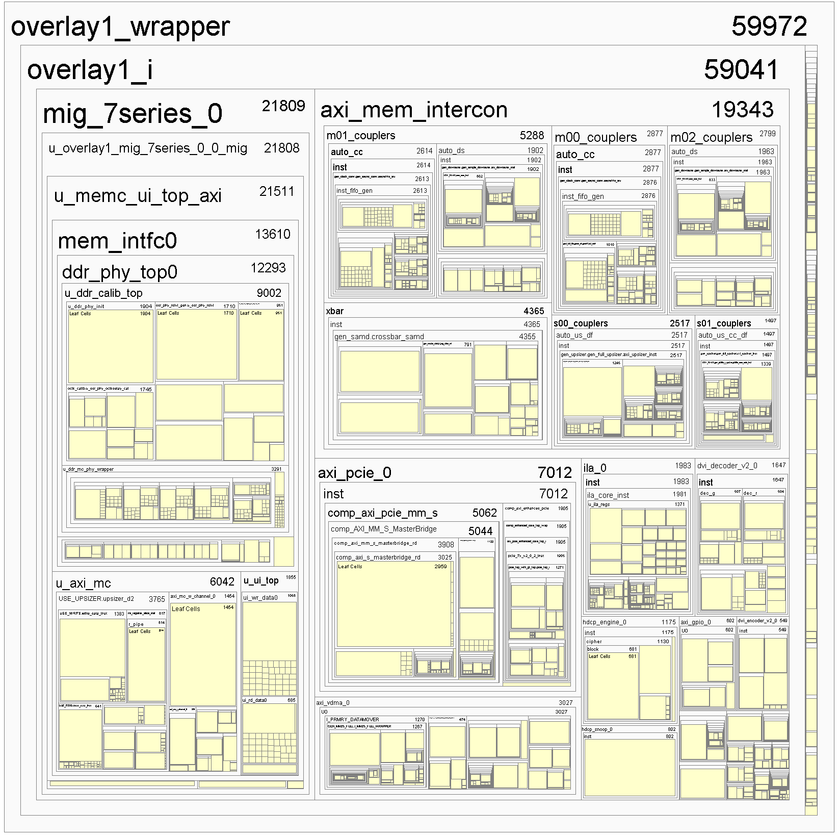
Below is the “hierarchical” view of this NeTV2 FPGA design. About 75% of the resources are devoted to the Vivado IP blocks, and about 25% to the custom NeTV application logic; altogether, the design uses about 72% of the XC7A50T FPGA’s LUT resources. A full-custom implementation of the Vivado IP blocks would save a significant amount of area, as well as be more FOSS-friendly, but it would also take months to implement an equivalent level of functionality.
Significantly, the FPGA reference design shared here implements only the “basic” NeTV chroma-key based blending functionality, as previously disclosed here. Although we would like to deploy more advanced features such as alpha blending, I’m unable to share any progress because this operation is generally prohibited under Section 1201 of the DMCA. With the help of the EFF, I’m suing the US government for the right to disclose and share these developments with the general public, but until then, my right to express these ideas is chilled by Section 1201.
>
> This hybrid flow strikes a unique balance between the
> simplicity and intuitiveness of designing with a schematic,
> and the power of text-based scripting.
>
Adjectives far more colorful than ‘unique’ spring to mind after having used Vivado’s IP {dis}Integrator on a few large designs across major Vivado versions.
Specific Gripes:
– Using the ‘schematic’ mode for incremental edits on a large block design regularly corrupts the design, often requiring a fresh start with a new project file.
– Tcl scripts to create IPI Block Designs using Xilinx IP are frequently non-portable between Vivado versions.
— Undocumented internal properties of the IP being manipulated in tcl tend to change without notice in the new Vivado releases, forcing one to painfully debug the worked-with-the-old-release tcl scripts.
— I have no objections to tcl for tool scripting, but forcing designers to do “high level” design entry in structural tcl with an objects-gone-wild design philosophy isn’t my idea of a good time.
– Xilinx IP within a BD must always be updated to the latest version to make any changes to a design (which creates many of the maintenance/portability headaches).
– The Out-of-Context flow, needed for large designs, is crippled to a bottom-up-only implementation.
– Top level IP ports are limited to the basic plain-old-Verilog types; no records/structures, user defined types, etc. Even real generics (long supported in the older ISE XPS) are verboten.
– No SystemVerilog/VHDL-2008 is allowed at the top level for packaged IP.
– Packaging existing working and tested XPS pcores with the Vivado IP packager is a horror show of forward incompatibility/crashes/non-existent documentation.
The best organized public examples I’ve spotted of tcl scripted IP designs using Vivado are the ADI reference designs:
https://wiki.analog.com/resources/fpga/docs/hdl
-Brian
Hi, excellent blog post. Many thanks for sharing this article below.
I truly took pleasure in reviewing your post as it was really useful to those who
are in the field of ASIC, FPGA and also semiconductor areas.
Maintain the hard work.