The Ware for May, 2006 is a little bit different. This time, I’ll tell you what the ware is, but your challenge is to tell me what specific components do.
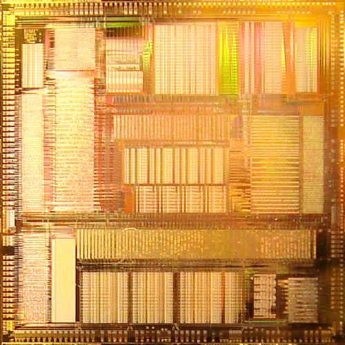
This month’s ware is the SGI “PG” chip from the original Reality Engine graphics supercomputer from back in oh…1992-ish. I believe this chip was responsible for polygon generation, hence the acronym PG (I could be wrong, anything over a decade old–heck, a day old–in my brain is liable for bit-rot). I got these chip samples when I used to work for SGI many moons ago, back on their follow-on product to the RealityEngine2 (before it got canned and all the key employees went their separate ways to start or to work at these crazy companies called nVidia, ATI, and 3dfx, all trying to bring graphics to the desktop. Actually, it was this first-hand observation of people movement correlated to the subsequent decline of SGI and the rise of the new graphics companies that convinced me that people are the most important asset of a company, and that individuals can and do matter, even in big organizations).
Since I have silicon on the hacking brain this month, I figured it might be fun to try and challenge readers with some wares that you just can’t look up in google to get the right answer. For first-time silicon hackers, I have a short tutorial on how to read chips.
There are three categories for the ware, just in case it is too easy or too challenging for people. I have one easy ware, one medium ware, and three “hard” wares. I am able to identify the easy and the medium ware with direct visual inspection (hint: they are fundamental logic gates). The three hard wares I suspect what their function is, but I would have to spend some time with a pencil and paper to trace out the circuitry and then try to deduce their precise functions based on the circuit diagram (and it’s quite possible that I couldn’t figure out what they do even after that). Of course, you are operating without the benefit of being able to infer function from the larger context of the overall chip, but the good news is that this is a very old-fashioned 2-layer metal design so almost all the transistors are visible in these photos. I will give out multiple prizes, one for each of these wares, and you can win multiple times (check the rules for the prize possibilities!). So with no further ado:
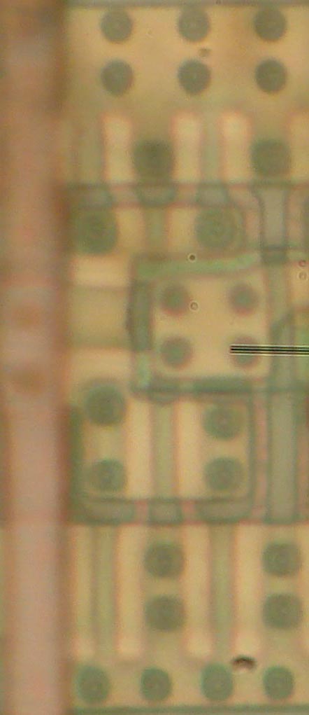
Easy (left) Medium (right)

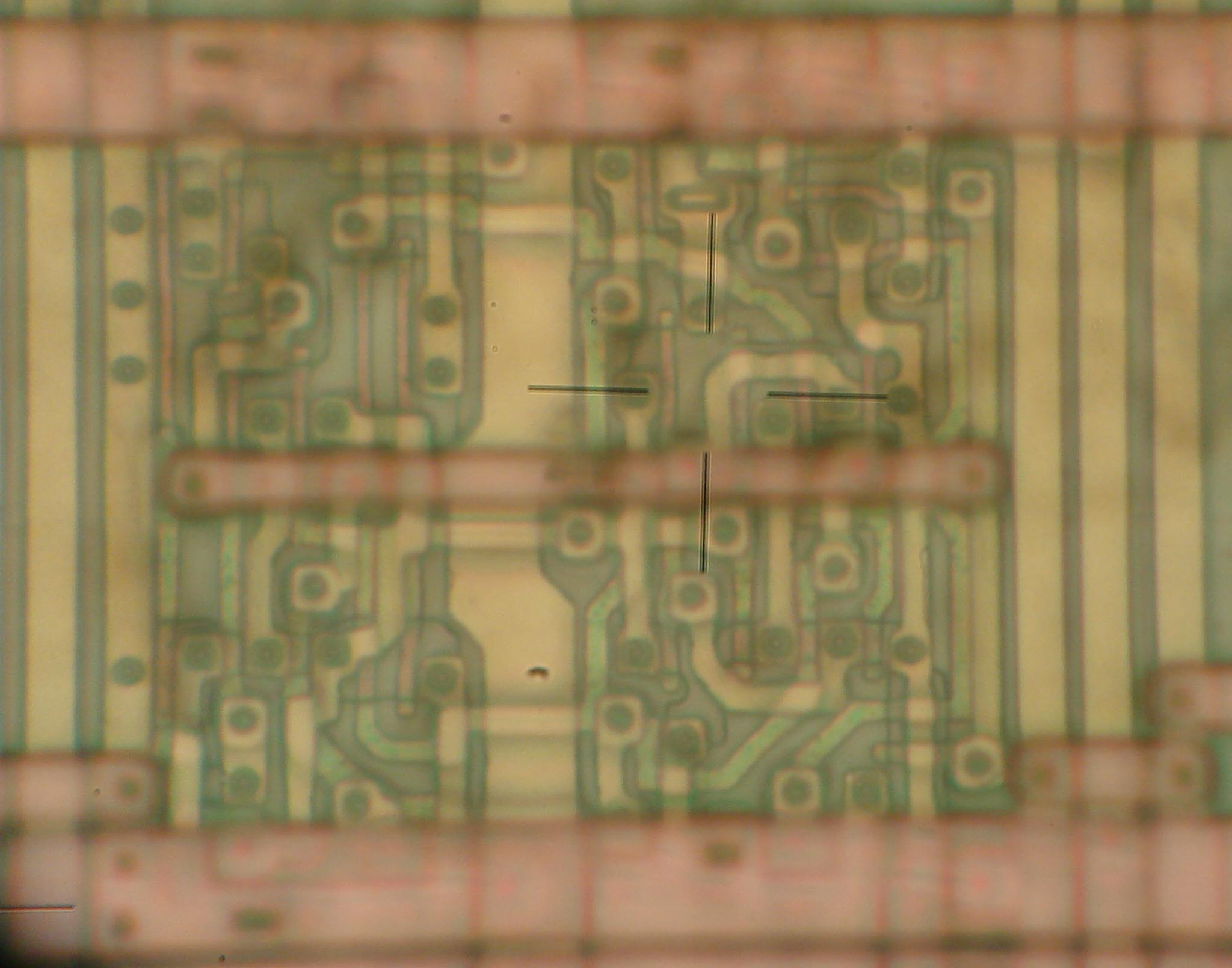
Hard (1)
Hard (2)

Hard (3)

good luck, feel free to discuss and ask questions…I will help with hints if people need them.
Could the medium ware be an inverter or a buffer?
Seriously, I am not even sure where the transistors, and the easy ware looks like an inline 5 engine block to me.
I am really interested, and I want to learn more about silicon reading.
Can you give me some directions bunnie?
Wow bunnie… we’re getting obscure! You may think I’m the silicon idiot, but now I’m going to prove it.
The “easy” one I’m going to guess is an inverter or buffer… I think I’m seeing horizontal Vcc and Ground metal on the top and bottom, a gate line coming in from the left, and an output going out the right.
Are there five transistors on each side? I’m guessing in parallel to handle the current needed on the output….
Ok, I’m a total novice reading chips, but I’ll start with the easy one, please somebody correct me if it’s total nonsense.
I assume the copper-coloured things on the right and on the left to be two metal layers near the surface. There are deeper-burried metal layers (‘gold’ color) that go horizontal. One on the top, one on the bottom, a C-shaped one left and a Y (rotated 90° clockwise) shaped one right. The C-shaped one is connected with 2 vias to the left copper-metal, the Y-shaped one with 2 vias to the right copper meta.
There is a blob of polysilicon under the stem of the Y-shaped metal connected with 5 vias (why so many???) and the vertical fingers coming out of it lay on top of a ndiff or pdiff that is connected to the upper, lower and C-shaped metal layer so that two classes of parallel fet-transistors are built:
(1) Drain=Top, Source=C-shaped, Gate=Y-shaped
(2) Source=Bottom, Drain=C-shaped, Gate=Y-shaped
So it could in principle be a inverted with the input being the Y-shaped metal on the right and the output being the C-shaped metal on the left, the supply voltages would then be the upper and lower golden layers.
Now that does not sound professional or even convincing, but it’s the only suff I could come up with up to now… :-)
Wow, I had a spate of spam comments recently, and I didn’t even realize I had comments on this post, they were so buried in the spam. Sorry about the slow moderation.
jimmyjo — the medium ware is an inverter, correct.
roastbeef–actually, so is the easy one–I was just taking a more careful look at them and I realized both are inverters (I originally thought the medium one was a NOR gate but then realized I was confused, I only looked at the polysilicon patterns and didn’t bother tracing out the diffusion when I picked the images). And indeed, yes, those are five gates in parallel to make a “bigger” buffer without destroying the aspect ratio of the device, since all the gates and devices sit in a “standard” cell height, like the moveable type on an old-fashioned printing press.
Christian–yes, the copper-colored things on the edges are top layer metal. you are also correct in deducing that there is a “gold” metal layer that runs deeper. The top and bottom metal runs are power and ground respectively. You can tell the top one is power because the transistors are longer, and p-channel transistors are always longer than n-channel transistors to compensate for the inherent lower mobility of holes over electrons in these types of junctions. The blob of polysilicon is connected with multiple vias because the vias are so tiny, they have significant resistance; putting several in parallel reduces the resistance *and* improves yield (if one via were to close, for example, you still have four to back you up! and when you have a million vias on a chip, you bet some of them close up). So your analysis is spot-on! good work!
I’ll post up some hint pictures over the next week to help gain some confidence in viewing transistors versus metal, etc.
awesome job guys!
I’ll try myself on the hard(1) mystery.
First, I think there is a nwell in the upper half of the picture (roughly seperated where the middle horizontal metal (copper coloured) goes). The gates in the upper half all look considerably larger than in the lower half which means pmos that is a pdiff sitting on a nwell.
I’ll try to explain the geometry a little, even if it will be quite tedious to read due to my limited vocabulary as a non-native speaker :-).
There is a large, C-shaped pdiff on the upper-left. One really long poly-finger near the 2nd big vertical metal, 4 small ones coming out from under the horizontal-copper-coloured metal, one small finger coming from the top (near the 3rd bigger metal on the left side).
One big straight p-diff is on the right, directly above the middle horizontal copper-coloured-metal and two smaller ones just below the upper big horizontal metal.
The lower half has two ndiffs, a straight one on the left with 5 poly fingers sticking in, the right one has 6 gates and is kind of “t”-shaped.
I think could identify almost all transistors (counting 1 transistor per gate), but the resulting schematics do not make any sense to me. The only thing I really could identify is one NAND gate built by the small upper-right ndiff and the lower right part of the lower-right “t”-shaped ndiff:
The nmos-transistors (bottom) are in series, the upper p-mos are parallel. Inputs are the two longish metal and poly on the right hand side, output is between the fingers of the upper p-mos (then follow the metal down to nmos).
I think I also found an inverter inside the two bigger p/ndiffs on the right. The 2nd gate/poly finger of both (counting from the left) are connected to each other, that’s the input and the diff on the left is contacted by what I interpret as Vcc/GND. The diffs on the right are also connected to each other and form the output.
The other transistors conenctions I don’t quite get, even after shuffling them around in a schematic for some time. They exhibit some symmetry, simmilar grouping of pmos and nmos transistors, with gates permuted in a somehow logical way) but I am not able to determine something like a truth-table from it.
Nevertheless, I think I found a basic logical gate that (according to the definitely not equal schematic) somehow matches the amount of transistors, has an inverter and a NAND gate :-)… So my guess is, it’s a…
69488af51235d5ff68d0f0800be3e104 (md5sum).
The tools I used were gimp for making a higher-contrast version of the picture and using the layers feature to colour diff/poly/metal and xfig for drawing schematics. And thanks Bunnie for this really entertaining Name-That-Ware, I’m enjoying it.
Christian — can you send me your plaintext guess (or post it) now that the contest is just about up? I doubt I’ll be able to hash-collision it :)
thanks!
Ok, so my guess is a “full adder”, a device that has A, B and Carry as inputs and outputs the numbers of set bits as a 2-bit number.
I was not able to really make sense out of the schematic I reconstructed from the microscope pictures but looking at the connections between the transistors (simmilar structures, with gate inputs somehow permuted) I guessed that it implements some small truth table. Comparing with the transistor-level schematic of one 1-bit full-adder I found on the web, the number of transistors and the “symmetry” in the layout somehow matched features I think are in your ware.
wats this all about
[…] The past two Name that Wares were fairly easy, so I thought I’d make this one a little more challenging — and yes, this month I can offer again a dent-and-scratch chumby as the prize! This one involves silicon reading — for those unfamiliar with the art of reading silicon, check out May 2006’s name that ware and the primer post (has this competition really been going on for that long? I should make a picture calendar of past Name that Wares). […]
Great post! Just wanted to let you know you have a new subscriber- me!