The ware for August 2010 is shown below. Click on the photo for a much larger version.
Taking this ware apart was particularly enlightening because I had thought about building one of these myself quite often, and now that I see the insides I realize I had over-complicated my schemes.
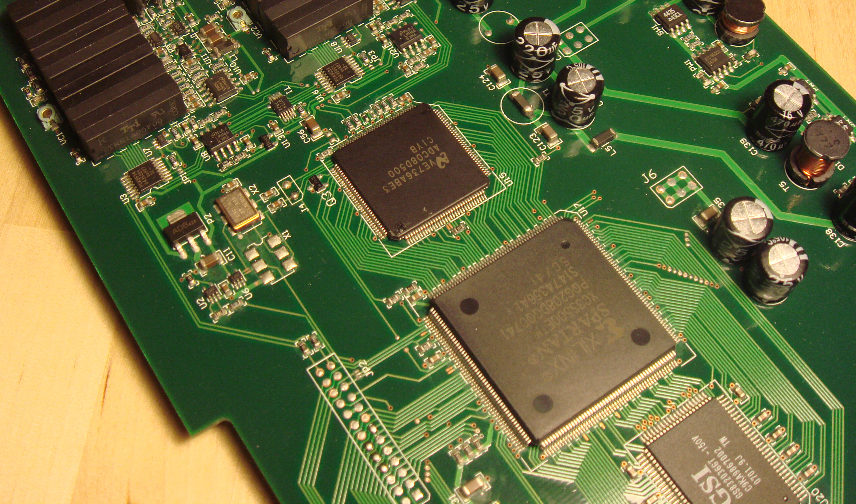
It is a dual channel analog to digital converter attached to an FPGA. The boxes at the top are relays. Given all of this, I’d say it is a digital oscilloscope.
I think that’s likely as well. The notch along the bottom looks like clearance so you can put an x1 PCIe card in an x16 slot (or some combination of x## card in slot), so I’m going to guess it’s an internal PCIe scope.
Similar logic to Devlin, but I’m going to go with a logic analyzer.
GSI chip is SRAM, probably for buffering analog reads. Can’t figure out what the blocky things are in the top left. I’d go with some digital recording equipment. I doubt it is anything high-frequency since nothing is shielded and traces aren’t equal length.
The cutout notch makes it look like a plug-in card of some sort. The Xilinx chip is probably a big FPGA of some flavor. I don’t recognize the other chips off the bat. The chunky vertical SIP/ZIP chips might be VRAM or relays. The UR logo tells me they’re relays. They’re surrounded by a lot of support circuitry, including little variable capacitors. Hmm, very analog feel. The board layout has a cut-and-paste look to it (the SW1/PW1 power block, with another one near it that looks like SW4/PW4). That, and the monolithic capacitor sitting in an electrolytic silkscreen makes me think this is a low-runner board. Doesn’t look like hi-fi or precision, so I’m gonna guess this one is a digitizer/data logger of some flavor.
The big NatSemi is a 500MSPS dual channel ADC. It’s connected to a 500MHz crystal, so they’re sampling at it’s rated speed. 500Mhz sampling rate is a too high for any reasonable analog function, but still within the realm of analog video.
That GSI chip, as mentioned, is a high speed synchronous burst SRAM. Those are definitely all relays, there’s no question there.
That’s a Spartan 3E there in the center. With 500k gates, there could be just about anything in there.
If it’s a DSO, why are there so many relays for inputs? Which brings me back to the AV stuff. I’ve seen video analyzers with that many inputs, before.
My bad… that was supposed to say “too high for any reasonable *audio* function”, not analog.
Just guessing another posibility still not said here: may it be a video surveillance card?
Digital stuff
– ADC08D500, I can’t read the xtal, but according to the datasheet it can’t be clocked lower than 200Mhz
– Spartan 3E with 500K gates
– GSI burst ram
Well, the digital stuff has been mostly worked out, so let’s look at the analog front end.
– LM6550 Differential high speed op amp 400Mhz bandwith
– LM6643 Dual rail to rail op amps 130Mhz bandwith
– PCA9534 is an I2C IO expander probably used for controlling the relays
– D7747 not sure, silkscreen says TI, and gets the output of one of the 6643’s. Maybe something to do with power for the analog stuff?
– 7! relays per channel, appear to be used as attenuators, not to switch between inputs.
– Bunch o passives as a filter
There’s also a glimmer of a connector/s at the far top (the through hole parts). You can only see pins, and based on the length of the relays, that must be a long connector, maybe 20-25mm long. Or it could be some kind of magical passive I haven’t seen before. Or it could be diodes for a diode mixer? Or it could be status LEDs (have seen it on capture cards before).
So, there is some weird stuff going on.
– Looks like a cut and paste design, they nearly used the national semi app notes to design it.
– The layout is fairly spread out and the SMT tech is not very small. 0603s and QFPs are as fine as they get. Based on the number of visible traces on the top, it could be a two layer board, probably a four layer board. Looks almost like a prototype board I would make.
– There is not enough bandwidth in the op amps to see more than probably 400Mhz, the lower bandwidth op amps are probably used for a low noise linear power supply.
– There is no offset voltage, strange for a scope, maybe not so strange for a capture card? Maybe that’s what D7747 is for?
– There are no RF parts visible. No mixers etc for a software defined radio. This rules out that.
– How does the data get off the card? I don’t think Spartans can do PCI express, I don’t see an Ethernet PHY, USB is too slow for that kind of bandwith / Spartans would need some kind of phy to interface to usb (3V max IO logic). Could of course be a plug in for some instrument and have a proprietary bus.
– I thought that there aren’t enough lines free on the FPGA to be a PCI controller, but if you look at the top of the FPGA, there a bunch of signals that go to vias and if you count those and the ones on the bottom, you get around 35ish signals. You need around 40 for PCI so I could be missing some. Still this brings up another problem. That would be one hell of a FPGA design to deal with the ADC and the PCI stuff in only 500K gates. Also, dealing with clocks (seems to share the ADC clock) would be hellish because of the PCI clock.
– Also, what about bandwith? 500Ms/S at 8 bit does not fit on a PCI bus (133Mhz 32 bit wide), and two channels would definitely not fit. But what about triggering and storing a small sample in the GSI chip? Well…
– If we triggered and stored in the GSI chip, there should be some trigger logic. Where is it?
Looks like this would make a pretty terrible capture card for a computer. I don’t think there is enough muscle for PCI, (though this could be me over thinking it like Bunnie). Also, it seems if it were PCI, we would be able to see the connector in the photo.
Can’t really do a whole lot of RF without a bunch of external RF parts. I was thinking maybe a plug in card for an acquisition system (relays to switch between inputs – but see note about relays above), also having only 8 bits of precision is probably not enough for that kind of system.
So, I’m not too sure what this is. Mostly more confused than I was when I started this post – hence the length. I’ll think about it and post back.
D774 is a DAC7574, a 12-bit, 4-channel DAC. Not sure why they need 4 channels, but you can see the SPI lines going from the PCA9534 chips going to the right pins.
I’d go with a two channel usb attached dso. The BNC connectors are probably to the top left, the usb connector to the bottom right. There are some traces going in that direction. Note that you don’t need a high speed interface to the host, as you’re sampling periodic stuff and/or bursts. No need to stream 100msps to the host, thats what the sram is for. Trigger logic is probably completely in the fpga.
Unless they’re using one of the scope channels as a trigger, we should be looking for at least a DAC and a comparator. Probably also some op amps and maybe some fast logic too.
USB sounds good, but as I said we should be looking for some kind of phy. This could be small and on the bottom by the unpopulated connector, but there are far too many unaccounted for lines on the fpga for just usb.
There is a DAC (see above comment on D774), but I can’t really trace the lines. One of the outs definitely goes to the v+ input on the left 6643. There might be comparators on the other side of the board, or one of the opamps could be used as a comparator… I’m sure that all the logic happens in the FPGA.
I’m revising my guess to a hand-held, dual-channel scope. The chop be perfect for wrapping a ribbon cable around from the connector on the underside of the board to go to buttons on the case or LCD signals. Maybe non-volatile memory on the other side connected with all those vias.
my guess is that its a controller for a vendomatic. either a regular vending machine with a fancy display or a pacman like simple video game console like they have in arcades that takes coins.
could it be some sort of test switching module?
i dont see why you`d consider building one though
I’m not buying the notch being for PCI or anything similar.
First thoughts were an oscilloscope – the dimensions of the board looks about right for one of the newer portable digital scopes.
It’s not one of the cheaper scopes made by Rigol or GWInstek or the like – they all seem to use multiple 100Mhz or slower ADCs rather than one faster one.
The board does seem very spaced out, almost as if the size of it was constrained by something we can’t see (a display? a long connector?).
Most scopes do have relays for input attenuation, but they’ll always be in shielded cans. And not nearly as many of them!
I’ve not seen any video switching devices that use relays for a long time. But many years ago, it was common to see CCTV control units with large arrays of relays to switch the many cameras to a single screen or multiplexed screen. There are a load of ICs that do multiplexing though, and they will be a lot cheaper than a high-end FPGA.
Where are those 12 diagonal vias to the right of the FPGA going?
Not many answers there.
The date code on the GSI SRAM is 0701 (Week7 2001?). PCI-Express wasn’t around then! My guess – a pinball machine controller.
As indicated by the GSI logo, it’s a Graphical Scene Improver. This piece of equipment is used by forensics professionals over the world to analyze and extract information from low resolution surveillance video cameras. It is frequently shown in action in documentaries such as CSI or NCIS.
The central FPGA device is used to generate the display signals and compute the basic geometric primitives : mirror reflection, corneal reflection, windshield reflection and of course sunglasses reflection. Naturally these primitives can be combined as needed.
The National semiconductor ADC package is used to provide voice control and respond to the “zoom” and “enhance” commands within 2 nanoseconds.
The GSI chip is the heart of the system. It contains the proprietary smoke that allows the reversing of lossy compression algorithms to take place.
Finally the relays and other circuitry are used to create the clicking and sound effects that are the hallmark of any serious computing device.
Hope it helps.
@vic, your a funny man!
Hi, this note isn’t about a current blog, but it’s the only way I could reach you about some older photos on previous blogs.
My name is Gil Daspit and I work for the city government cable TV channel in Tallahassee. Two Chinese gentlemen visited Tallahassee as part of a fellowship program through the US State Dept. I am putting together a video about their visit and need some photos of China to illustrate some of the things our visitors talked about when I interviewed them.
I saw two pictures on your blog I’d like to use –
pcb_factory_sm. (from Sept. 12th, 2007) and
tooling 1 (From, Sept. 11th, 2007 ) is this ok?
Thanks, Gil Daspit Jr.
(P.S.: I’m writing from my personal e-mail, my e-mail address at work is Gilbert.Daspit@talgov.com)
Hi Gil,
The content on this blog is covered under a creative commons by-sa license. This means that you are free to use the work as long as you provide attribution and you apply a similar license to the derivative work.
thanks!