The Ware for November 2016 is a Link Instruments MSO-28 USB scope. Congrats to Antoine for the first guess which got the model number correct, email me for your prize!
Winner, Name that Ware November 2016
December 25th, 2016NeTV2 FPGA Reference Design
December 3rd, 2016A complex system like NeTV2 consists of several layers of design. About a month ago, we pushed out the PCB design. But a PCB design alone does not a product make: there’s an FPGA design, firmware for the on-board MCU, host drivers, host application code, and ultimately layers in the cloud and beyond. We’re slowly working our way from the bottom up, assembling and validating the full system stack. In this post, we’ll talk briefly about the FPGA design.
This design targets an Artix-7 XC7A50TCSG325-2 FPGA. As such, I opted to use Xilinx’s native Vivado design flow, which is free to download and use, but not open source. One of Vivado’s more interesting features is a hybrid schematic/TCL design flow. The designs themselves are stored as an XML file, and dynamically rendered into a schematic. The schematic itself can then be updated and modified by using either the GUI or TCL commands. This hybrid flow strikes a unique balance between the simplicity and intuitiveness of designing with a schematic, and the power of text-based scripting.

Above: top-level schematic diagram of the NeTV2 FPGA reference design as rendered by the Vivado tools
However, the main motivation to use Vivado is not the design entry methodology per se. Rather, it is Vivado’s tight integration with the AXI IP bus standard. Vivado can infer AXI bus widths, address space mappings, and interconnect fabric topology based on the types of blocks that are being strung together. The GUI provides some mechanisms to tune parameters such as performance vs. area, but it’s largely automatic and does the right thing. Being able to mix and match IP blocks with such ease can save months of design effort. However, the main downside of using Vivado’s native IP blocks is they are area-inefficient; for example, the memory-mapped PCI express block includes an area-intensive slave interface which is synthesized, placed, and routed — even if the interface is totally unused. Fortunately many of the IP blocks compile into editable verilog or VHDL, and in the case of the PCI express block the slave interface can be manually excised after block generation, but prior to synthesis, reclaiming the logic area of that unused interface.
Using Vivado, I’m able to integrate a PCI-express interface, AXI memory crossbar, and DDR3 memory controller with just a few minutes of effort. With similar ease, I’ve added in some internal AXI-mapped GPIO pins to provide memory-mapped I/O within the FPGA, along with a video DMA master which can format data from the DDR3 memory and stream it out as raster-synchronous RGB pixel data. All told, after about fifteen minutes of schematic design effort I’m positioned to focus on coding my application, e.g. the HDMI decode/encode, HDCP encipher, key extraction, and chroma key blender.
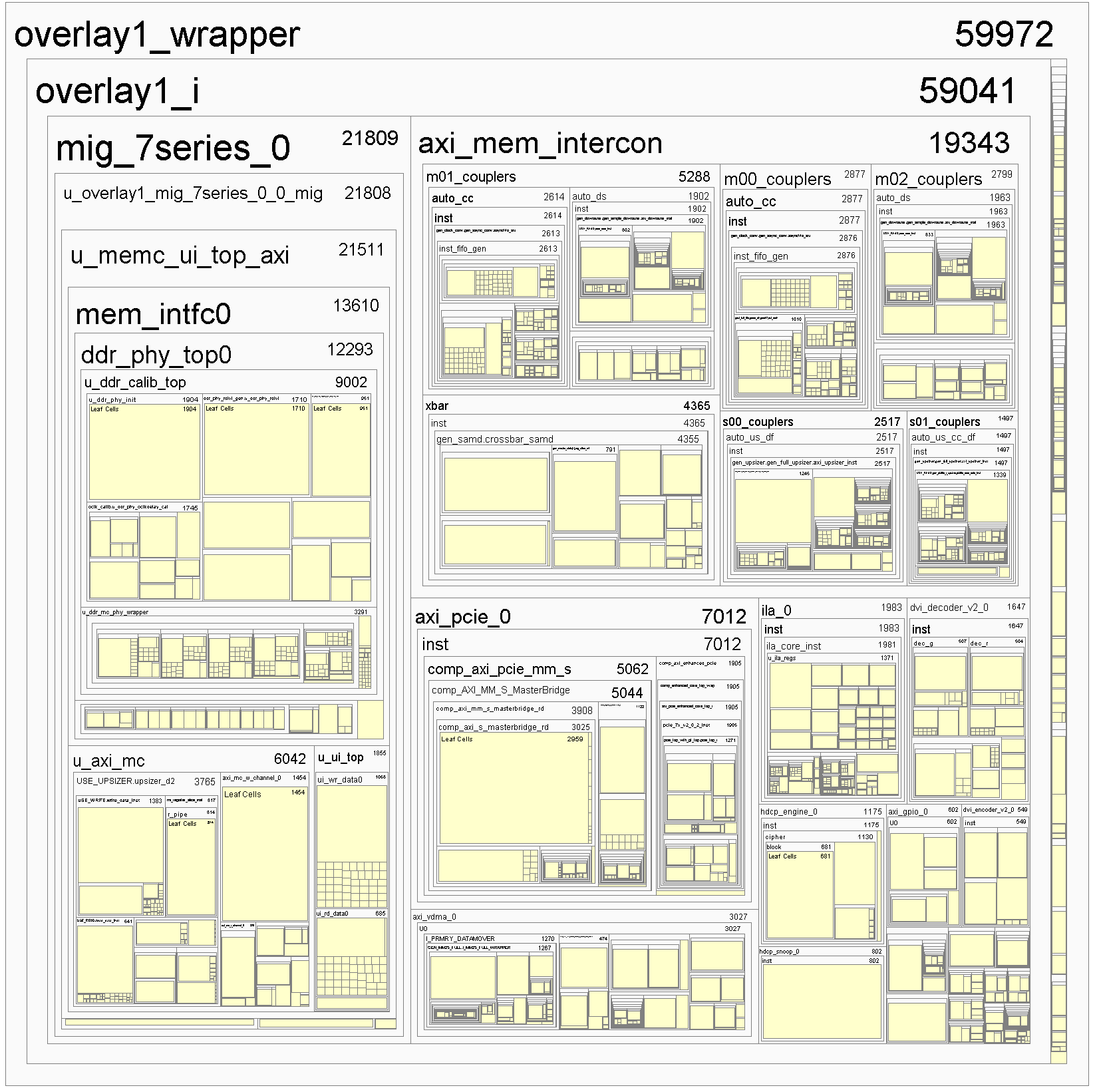
Below is the “hierarchical” view of this NeTV2 FPGA design. About 75% of the resources are devoted to the Vivado IP blocks, and about 25% to the custom NeTV application logic; altogether, the design uses about 72% of the XC7A50T FPGA’s LUT resources. A full-custom implementation of the Vivado IP blocks would save a significant amount of area, as well as be more FOSS-friendly, but it would also take months to implement an equivalent level of functionality.
Significantly, the FPGA reference design shared here implements only the “basic” NeTV chroma-key based blending functionality, as previously disclosed here. Although we would like to deploy more advanced features such as alpha blending, I’m unable to share any progress because this operation is generally prohibited under Section 1201 of the DMCA. With the help of the EFF, I’m suing the US government for the right to disclose and share these developments with the general public, but until then, my right to express these ideas is chilled by Section 1201.
Name that Ware, November 2016
November 30th, 2016The Ware for November 2016 is shown below.
Happy holidays!
Winner, Name that Ware October 2016
November 30th, 2016The Ware for October 2016 is a hard drive read head, from a 3.5″ Toshiba hard drive that I picked out of a trash heap. The drive was missing the cover which bore the model number, but based on the chips used on its logic board, the drive was probably made between 2011-2012. This photo was taken at about 40x magnification. Congrats to Jeff Epler for nailing the ware as the first guesser, email me for your prize!
NeTV2 Tech Details Live
November 1st, 2016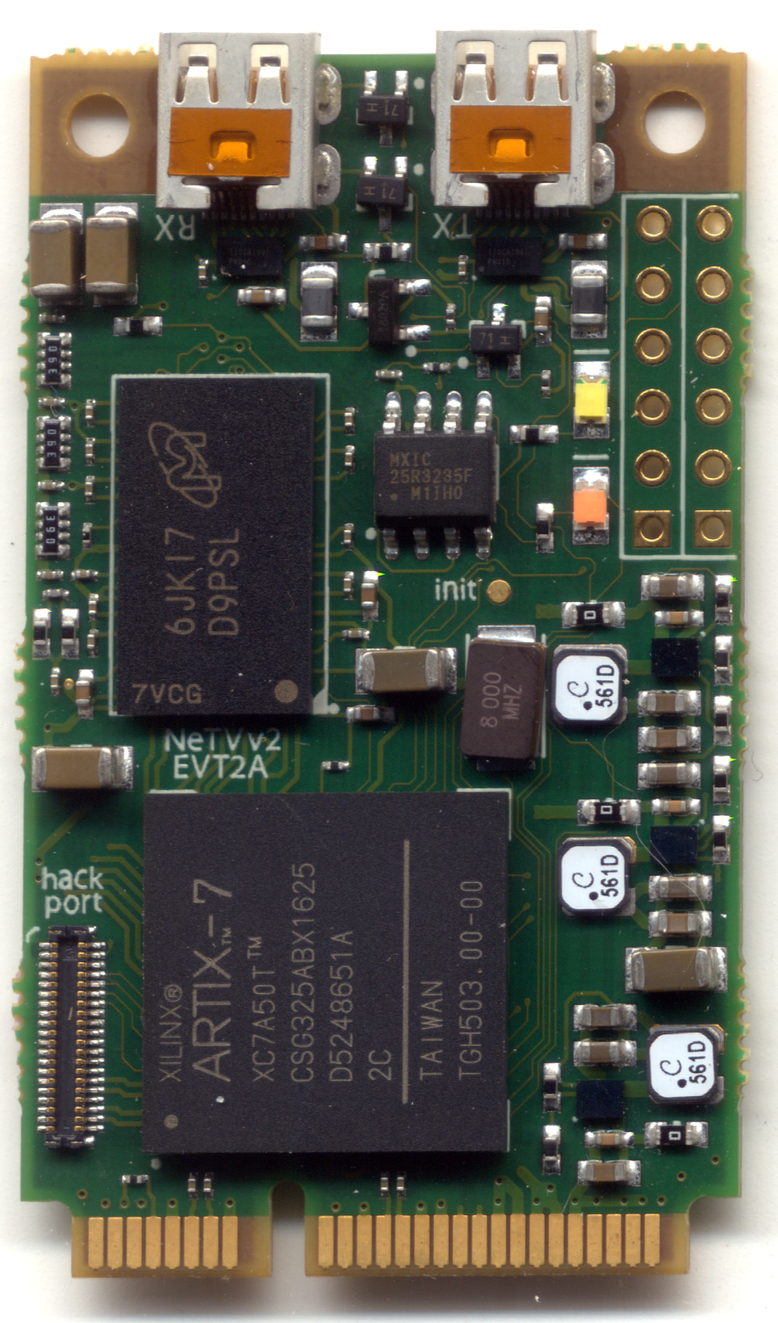

Alphamax LLC now has details of the NeTV2 live, including links to preliminary schematics and PCB source files.
The key features of NeTV2 include:
- mPCIE v2.0 (5Gbps x1 lane) add-in card format
- Support for full 1080p60 video
- Artix-7 FPGA
- FPGA “hack port” breaking out 3x spare GTP transceiver pairs
- 512 MB of DDR3-800 @ 32-bit wide memory for frame buffering
I adopted an add-in card format to allow end users to pick the cost/performance trade-off that suited their application the best. Some users require only a text overlay (NeTV’s original design scenario); but others wanted to blend HD video and 3D graphics, which would require a substantially more powerful and expensive CPU. An add-in card allows users to plug into anything from an economical $60 all-in-one, to a fully loaded gaming machine. The kosagi forum has an open thread for NeTV2 discussion.
As noted previously, we are currently seeking legal clarity on the suite of planned features for the product, including highly requested features such as alpha blending which require access to the descrambled video stream.
