I’m resolving some manufacturing challenges in the new chumby design and had the opportunity to use an X-ray board inspection tool. This tool is what you want to use if, for example, you wanted to reverse engineer a circuit board with buried or hidden traces. It also lets you see through the packages and inspect the quality of the wirebonds. This particular system has a feature that let you rotate the board as you inspected it so you can look at it at an angle–which is actually really cool to see live, it’s sort of like flying through the circuit board. I wish I had a video of it but I didn’t bring my camera into the shop today.
Anyways, I thought those who have never seen this capability before would find the following pictures interesting and perhaps thought provoking.

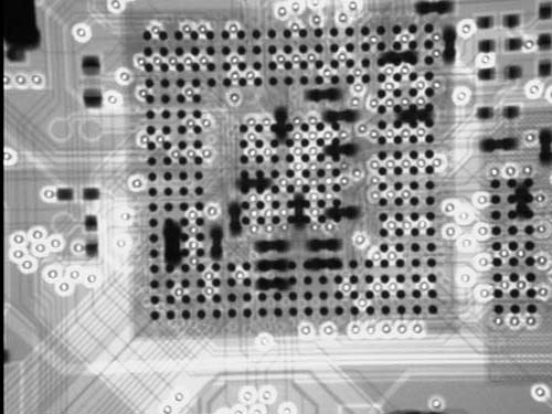
Nothing hides from the X-ray eye!
I find this also very fascinating. So much in fact, I use the X-Ray of my PowerBook as my background image.
http://usemycomputer.com/show.html?image=/indeximages/2006/January/31ec3058d34329421287e26db3bfc8f6.jpeg
http://www.albireo.net/powerbook/forum/gallery/showphoto.php?photo=625&sort=1&cat=502
http://www.flickr.com/photos/sudentas/236495126/in/pool-x/
Yeah, looks pretty interesting to me, I actually went ahead to the website (Focalspot) to have a quick look, they have those really cool camera on microscope steroids thingy…the images look amazing too….=p I’m staying away from BGA packages though…kinda hard for me to actually stick them on with what I have @ home…
Are those blobs under the MX21 BGA solder bridges? Can you also show what a dry joint under a BGA looks like on an X-ray image? Thanks
The blobs under the MX21 are the decoupling capacitors on the back side. They are less defined because they are slightly out of focus. This particular BGA device has seemingly perfect solder joints.
A dry joint has voids in it, which look like white spots or cracks in the X-ray view. There is an image enhancement mode in some versions of the Focalspot product that can help you spot these problems.
Is there a time limit for how long the various parts can be subjected to x-ray light? Are certain parts, like those that are flash programmable more susceptible to the radiation than parts that are hard wired?
That’s a good question. I don’t know the answer. I can tell you what I might expect.
Anecdotally, I have exposed parts with flash memory to x-rays for several seconds at least and noticed no degredation (I’m guessing my laptop, having been x-rayed through security checkpoints at least 40 times now, has gotten more than that dosage over its life). But this is by far not a reliable metric, because the chance that I actually notice one bit flipping in a few million is remote, especially with the ECC mechanisms is place on NAND flash. Eventually, the memory should degrade though, I imagine, since extended exposure to less energetic UV light should erase the parts even.
For non-memory parts, I don’t think there are any mechanisms that I can think of for them wearing out. x-ray absorption would create hole-electron pairs in the substrate but those should dissipate fairly safely, especially at these doses. The only time you’re in trouble is if you pound it with enough x-rays to generate a sufficient bias voltage that could cause device breakdown–maybe if you had some capacitor that was charging up ad nauseum due to the x-ray absorption current. I don’t think there is a mechanism for permanent crystal lattice damage directly because the x-rays are causing dopants to be displaced or anything like that. Parts are hit by cosmic rays and they survive that…
And:
http://www.phoenix-xray.com
I saw one of these that was in use for inspection purposes in the air force – the guy giving the tour took one persons watch and placed it in the machine. It’s very impressive to see a moving device through x-ray, it has to be said.
Couple of years later I found an x-ray machine in a skip. I have no idea when it dated from, but essentially it projected the x-rays over a table and onto a phosphorescent window. It wasn’t great, but it did work. I was extremely cautious and operated it from a distance, using a scope to view the screen. Eventually I took it apart to use the HT transformer for another project.
I was a manufacturing engineer in the aerospace electronics industry for several years. If you need help getting the bugs out of your process, drop me an email (I assume you can see my email).
Bit off topic bunnie but what wifi chip (dongle) have you chosen for chumby, and does it have Linux drivers or had to use ndis wrapper. I’ve just been messing around USB wifi dongles and the Prism2.5 works great but unlike the chumby does not support WPA.
[…] More PCB Stuff – Link […]
Re: x ray inspection time for flash memory:
I did some research on this as part of a report I’m doing for a company, and there are studies done in 2004 and 2002 by the IEEE on cumulative dosages for flash memory (as little as 5Krads (0.05 J/g of material). so working out the figures, it seemd that for a 1g flash memory IC, you have at least 1 minute of inspection time, but probably more like 2 or 3, before you should stop to aboid irreversible effects, even if these are not going to lead to hard failure. You can work it out by saying that at most, 2% of electrons in tube become photons, and then working out how many and their energy levels, plus taking into account that at say, 10keV, only 50% of x-rays are absorbed by IC. so there you go…