I recently had the pleasure and privilege of touring the factories that make Arduinos.
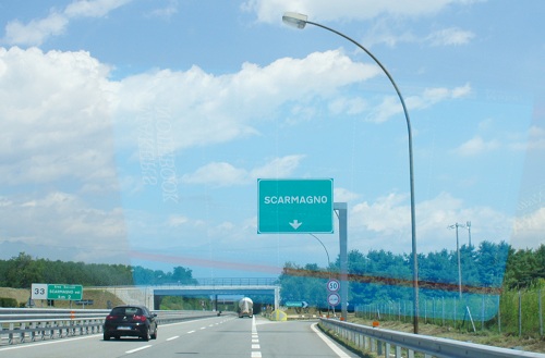
Arduinos are made in Scarmagno, Italy, a small town near the Olivetti factories on the outskirts of Torino. All of the circuit board fabrication, board stuffing and distribution is handled out of that small town. I was really excited to see the factories, and I’d like to share some photos of them with you.
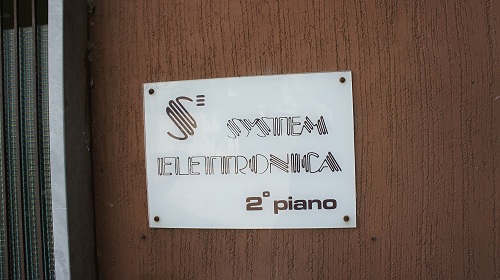
The highlight of my tour was “System Electronica”, the PCB factory which makes the Arduino PCBs.
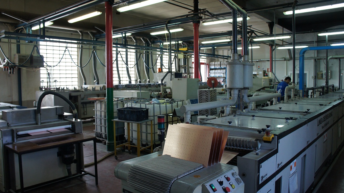
One charming aspect of System Electronica is the owner has the factory painted to match the colors of the Italian flag. In this wide view of the factory floor, you can see some of that in the red and white posts down the length of the facility.
Arduinos start as huge sheets of virgin copper-on-FR4.
![]()
The sheets above are 1.6mm thick (the most common thickness for a PCB, which corresponds to 1/16th of an inch), and probably a meter on one side by about a meter and a half.
The first step in processing is to drill the holes: hole drilling is done even before patterning. This is because once the holes are drilled, you can use the holes to align the masks used to pattern the traces later on in the process. Hole drilling is also a dirty and messy process, which can damage circuit patterns.
Above is the CNC drilling head used to drill the boards. The blank copper sheets are actually stacked three-high so a single pass of the drill can produce three substrates.

Above is the drill rack used by the CNC drilling machine. If you’ve ever had to muck around with creating NC-drill files, you’ll probably have seen the term “drill rack” used somewhere. This is what it looks like.
Above is the drill in action. It’s encoded in Ogg Theora; so, sorry if you’re using IE or Safari and you don’t have the codec installed. An HD version of the video is also available here. Flash is dead; long live HTML5! [note: I turned off video pre-loading to save bandwidth by just editing the attribute tags. That would have been a pain in Flash. Yet another benefit of HTML5!]
Every hole in the board is mechanically drilled, which is why via count is such an important parameter in calculating the cost of a PCB. This particular drill is a relatively small one. I’ve seen massive drill decks in China that slave four or six drill heads together in a truck-sized machine, processing dozens of panels at the same time; they drill so fast and hard that the ground shakes, even from several meters away, with every via drilled.
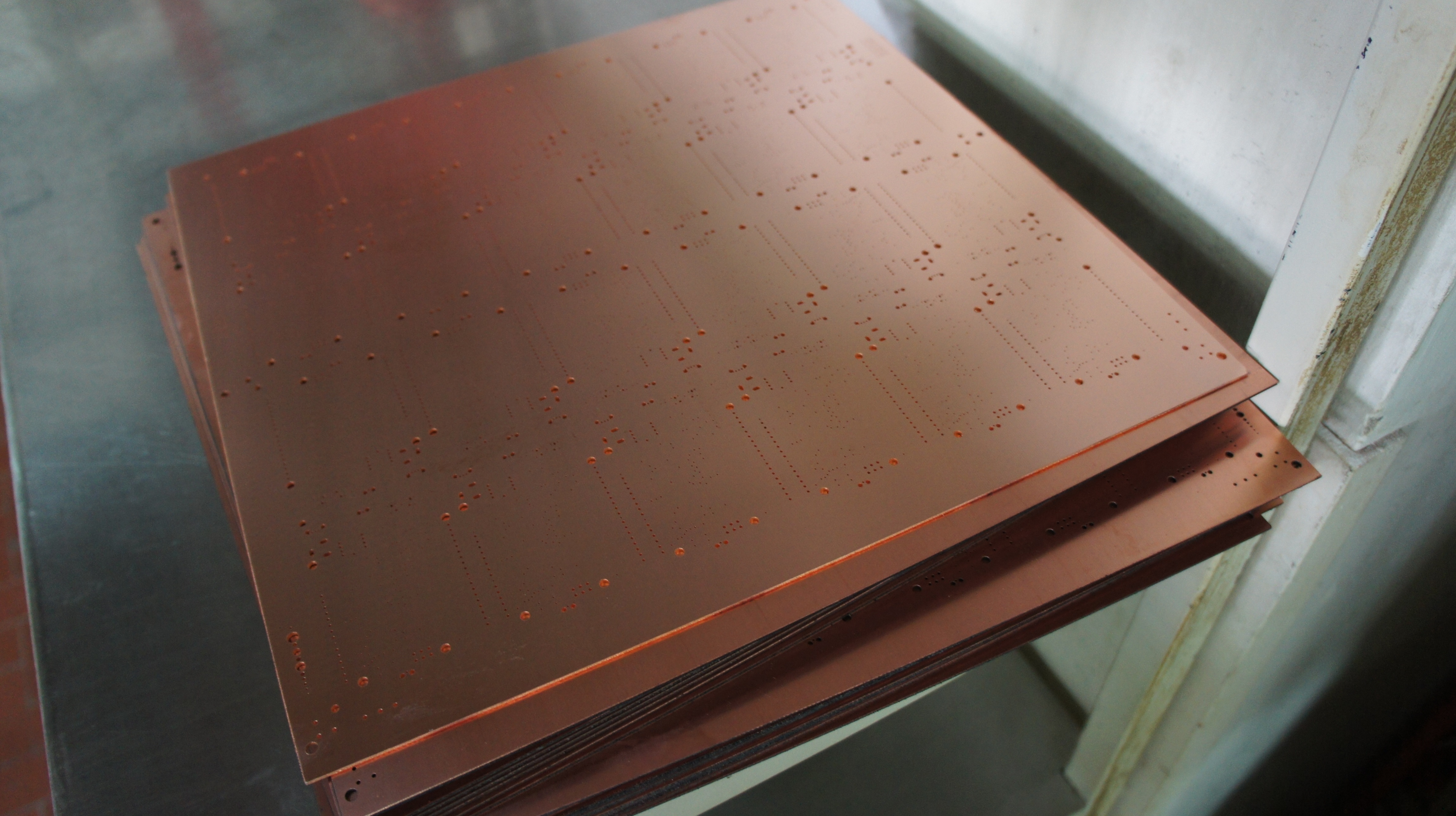
Above is a stack of finished, drilled boards that have been cleaned and deburred, ready for the next step in the process.
The next step is to apply a photoresist to the board and expose a pattern. At System Electronica, this is done using a light box and a high-contrast film. Other technologies I’ve seen include direct laser imaging, where the pattern is put on using a raster-scanning laser. Direct laser scanners are more common in quick-turn prototype houses, and film imaging is more common in mass production houses.
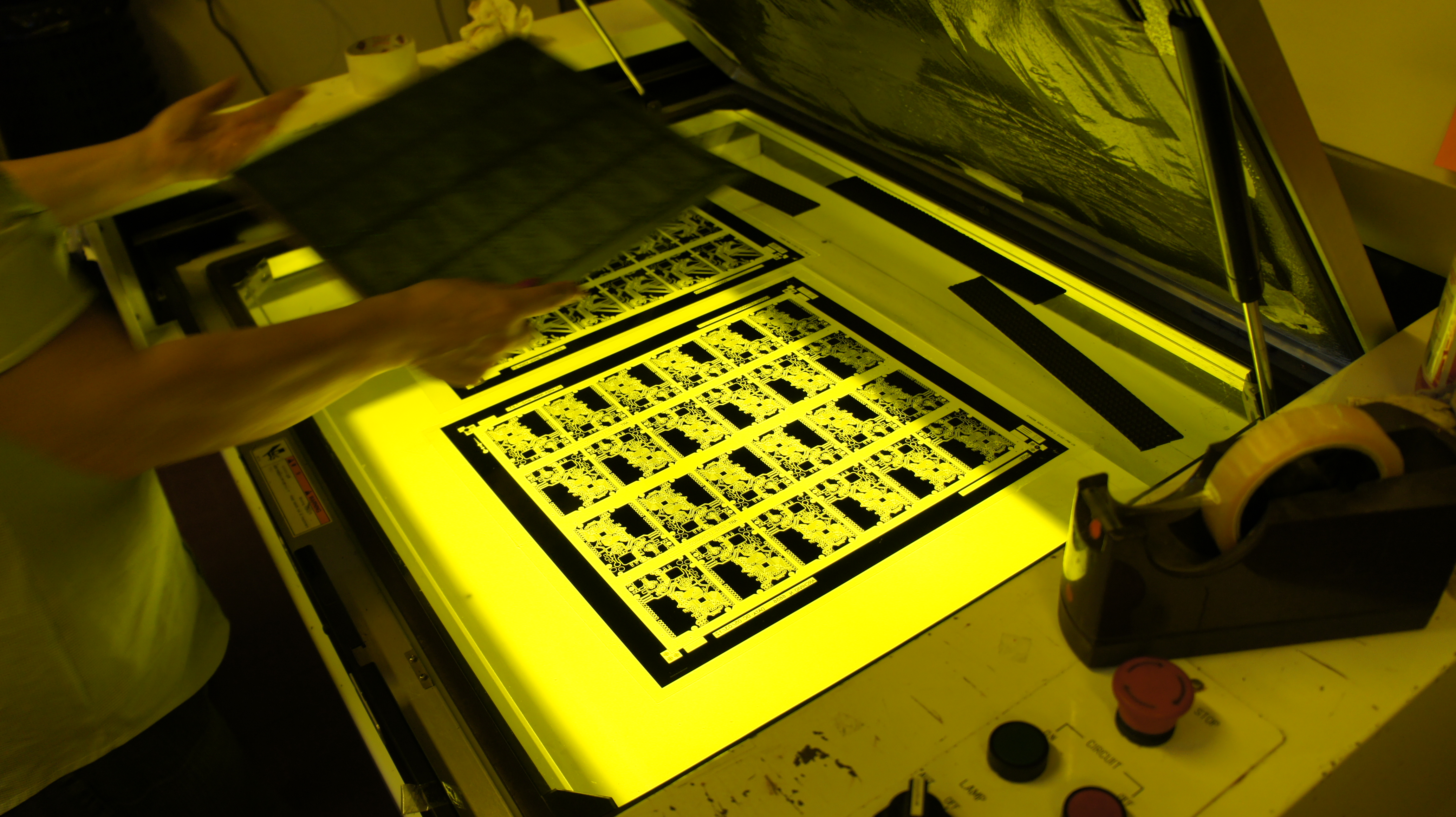
Above is a PCB blank being mounted into a light box for exposure. Note that most photos in this post can be clicked to reveal a much higher resolution version.
Above is what the board looks like before and after exposure.
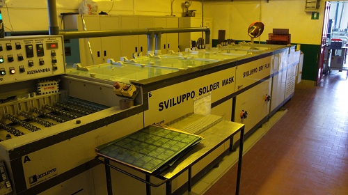
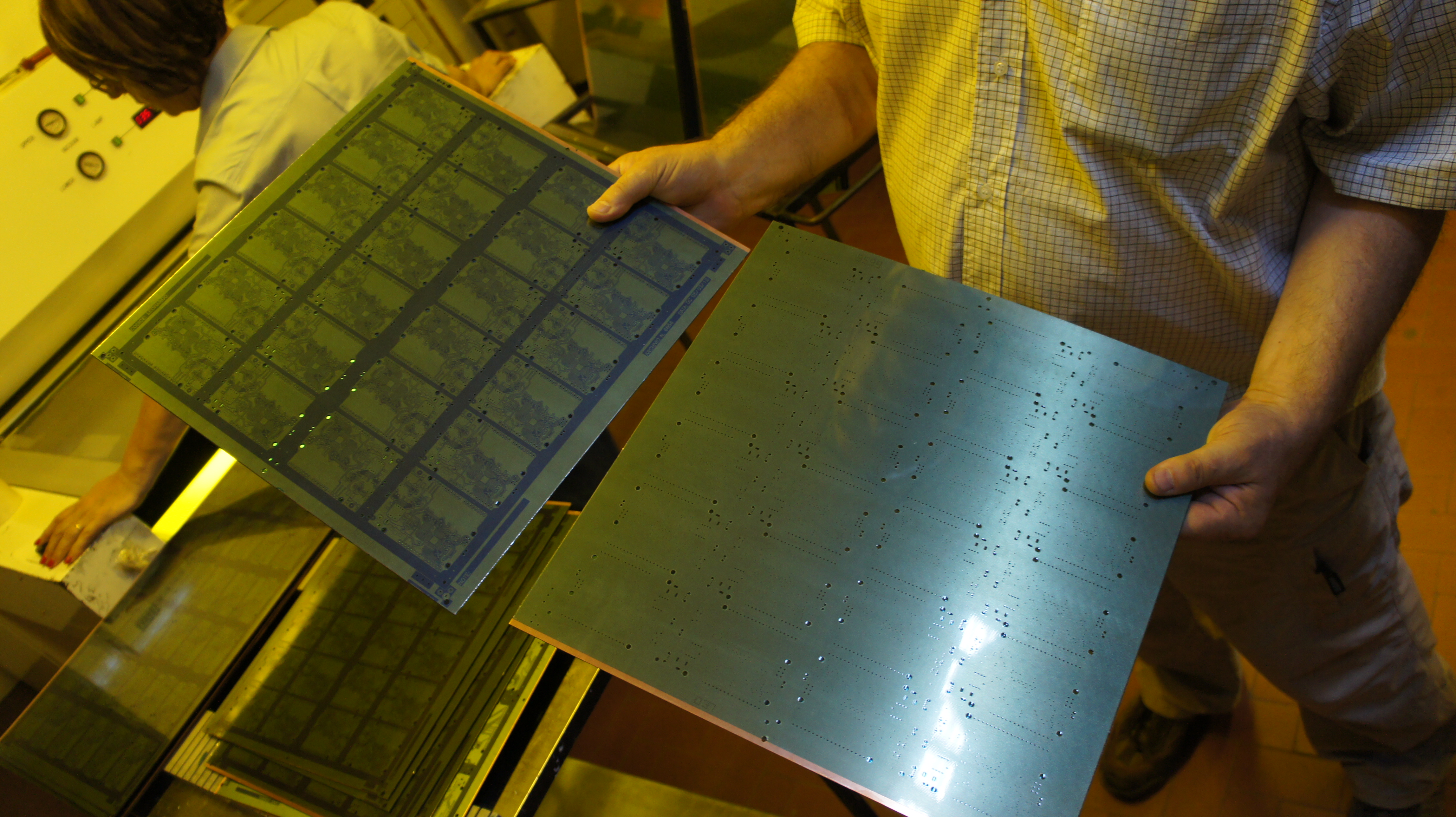
The boards are then sent into a machine to be developed. In this case, the same machine is capable of developing both the photoresist and the soldermask.

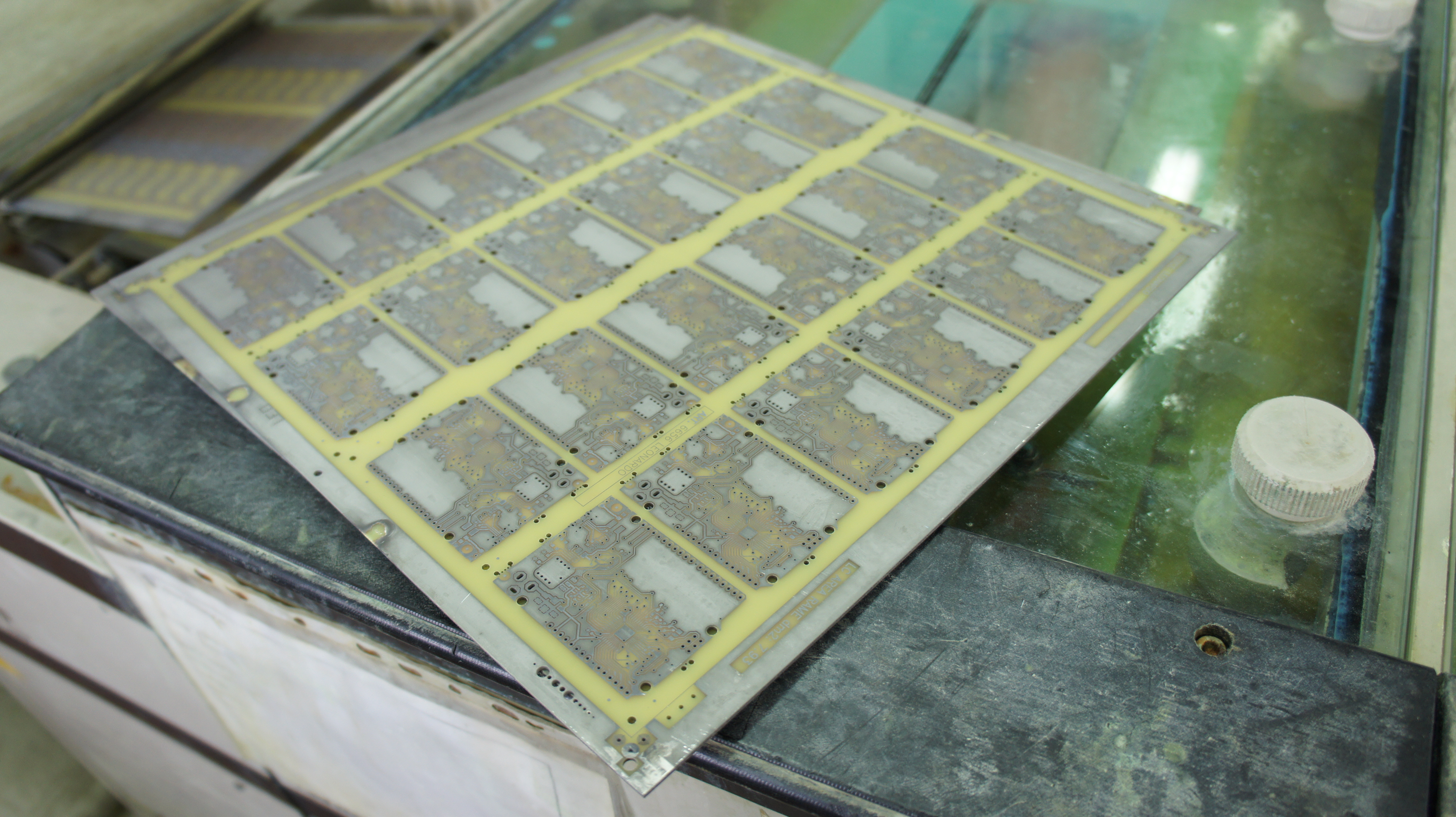
Above is an image of a developed board. It’s one of my favorite photos out of the factory. Also, there is just something cool sounding about “Codice: Leonardo”.
After photo-processing and development, the boards go through a series of chemical baths that etch and plate the copper.
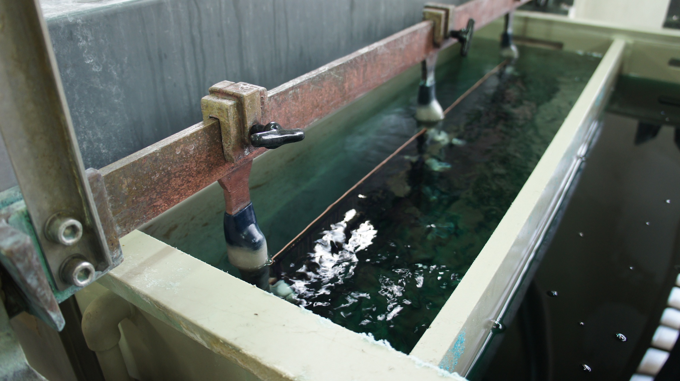
The movement of the boards through the chemical baths is fully automated; this is necessary because between certain steps oxygen can spoil a board in a matter of seconds, so the transfer between the baths needs to be fast. Also, the baths contain caustic and harmful chemicals to humans, so it’s much safer for a robot to do this work.
[HD verison] As you can see, the boards swish gently back and forth in the baths as they are processed. Each bath has a different solution in it.

Once the boards are processed in this series of solutions, a dull, white plating (which I’m guessing is nickel) has developed on all the non-resist covered surfaces of the board, including the previously unplated vias and pads.
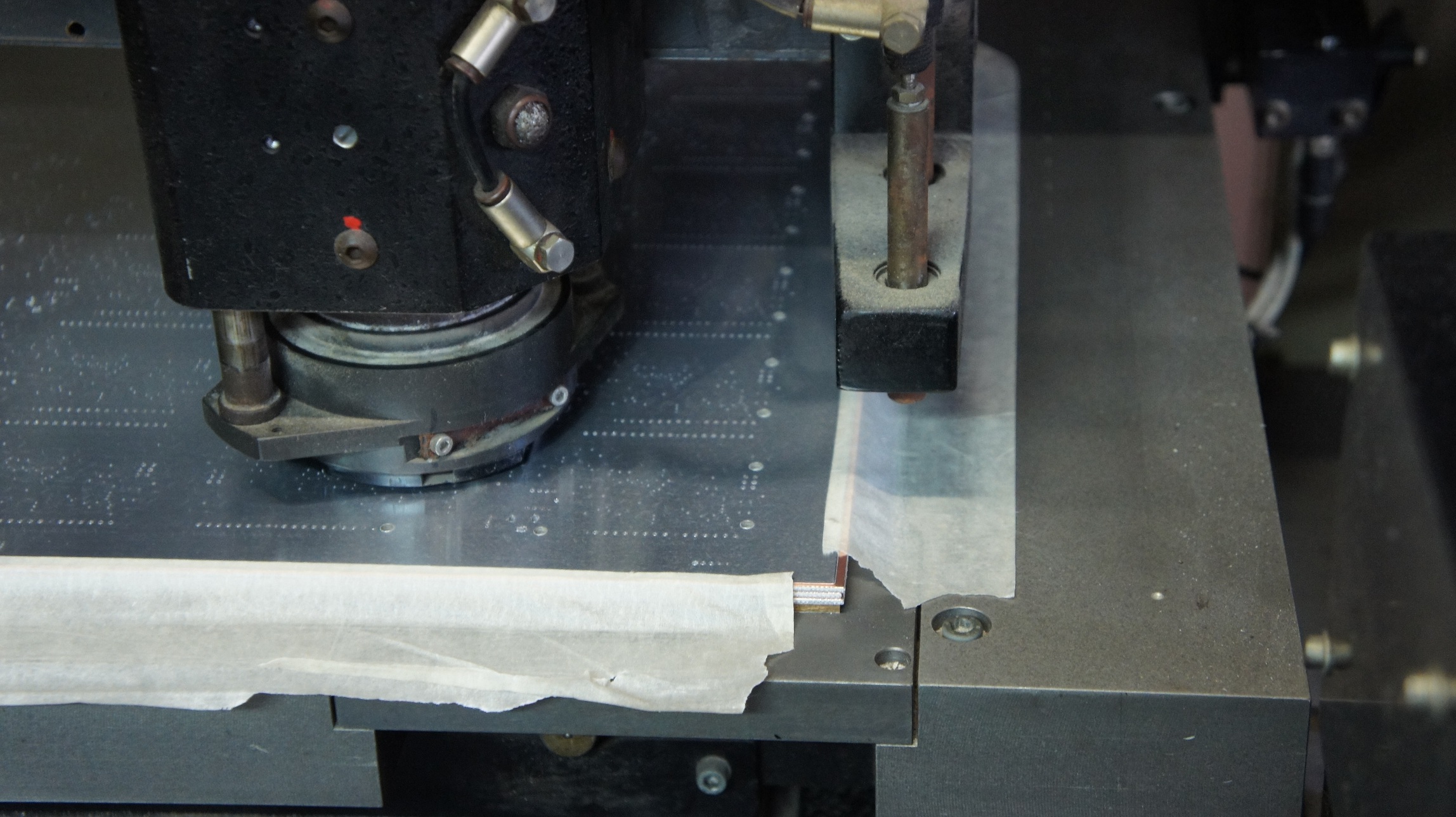
At this point the resist and unplated copper is stripped off, leaving just the raw FR-4 and the plated copper.

A final step of processing results in a bright copper finish. Note that the photo above isn’t of an Arduino board, as their boards weren’t going through the machine at the time when I was taking photos of it.
The boards are now ready to have soldermask and silkscreen applied. These are applied using a very similar process to the trace patterns, using a photomask and developer/stripper machine.

Above is photo showing a board with both soldermask and “silkscreen” developed. The silkscreen in this case is actually a second layer of soldermask. A very specific formulation of dry-film white soldermask was procured for team Arduino to create a sharp and good-looking layer that can resolve the intricate artwork found on Arduino boards. Other techniques I’ve seen for producing silkscreen layers include high resolution inkjet printing, which is better suited for quick-turn board houses, and of course the namesake squeegee-and-paint silkscreen process.
Once the boards have finished chemical processing, they receive a protective plating of solder through a hot-air solder leveling machine, and then move on to testing.
[HD version] Every board is 100% tested. This means that every trace has its continuity and resistance measured using a pair of flying probes. That’s a lot of probing, and the video above gives you an idea of how fast the probing is done. An alternative to flying head testing is to use clamshell testers, where a set of pogo pins are put into a fixture that can test the entire board with a single mechanical operation. However, clamshell fixtures are very labor-intensive to assemble and maintain, and require physical rewiring every time the gerbers are updated. So, in many cases flying probe testing can be cost-favorable and more flexible when compared to fixtured testing.
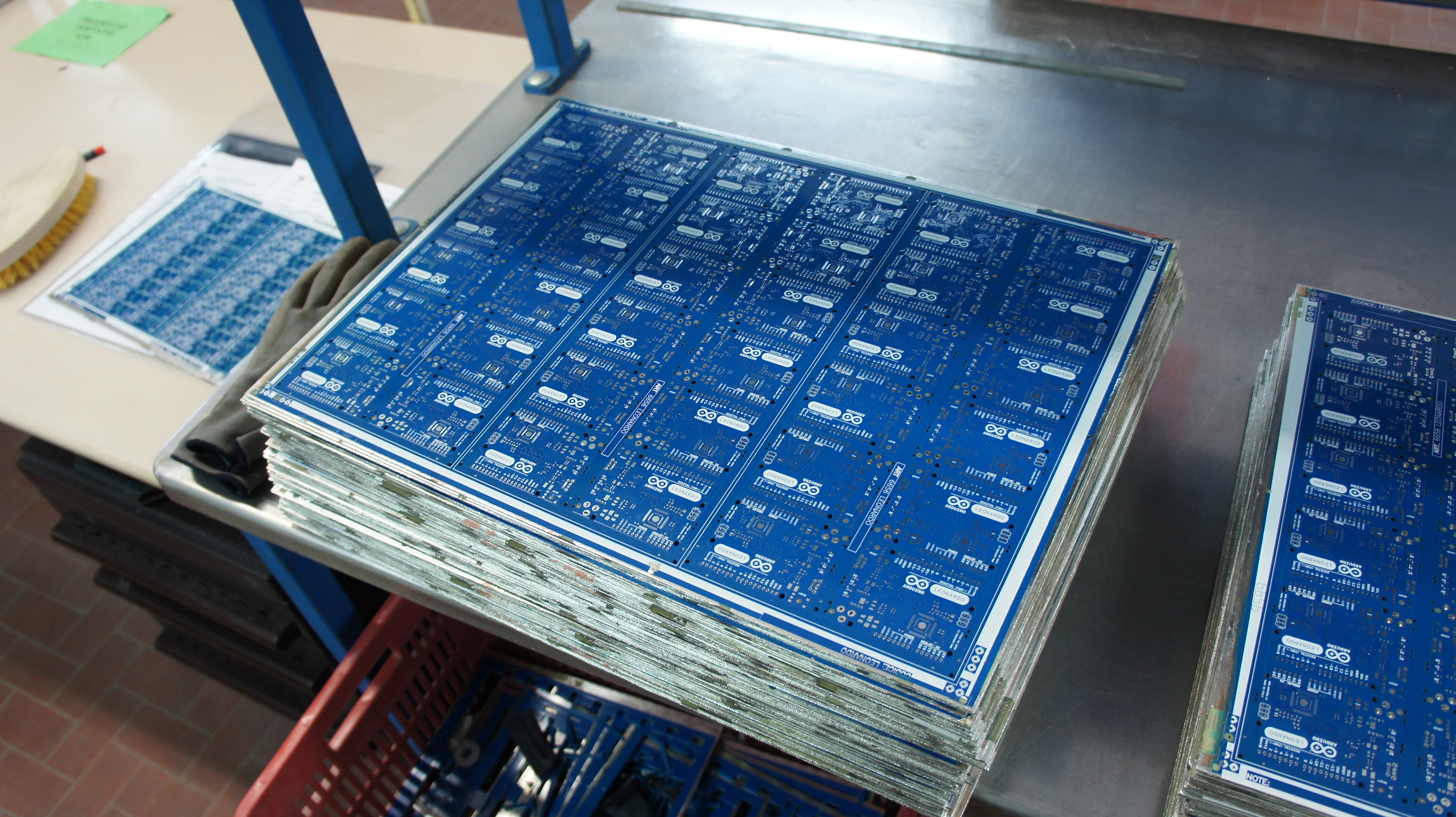
Above is a stack of near-finished PCB panels, ready for a final step of routing.
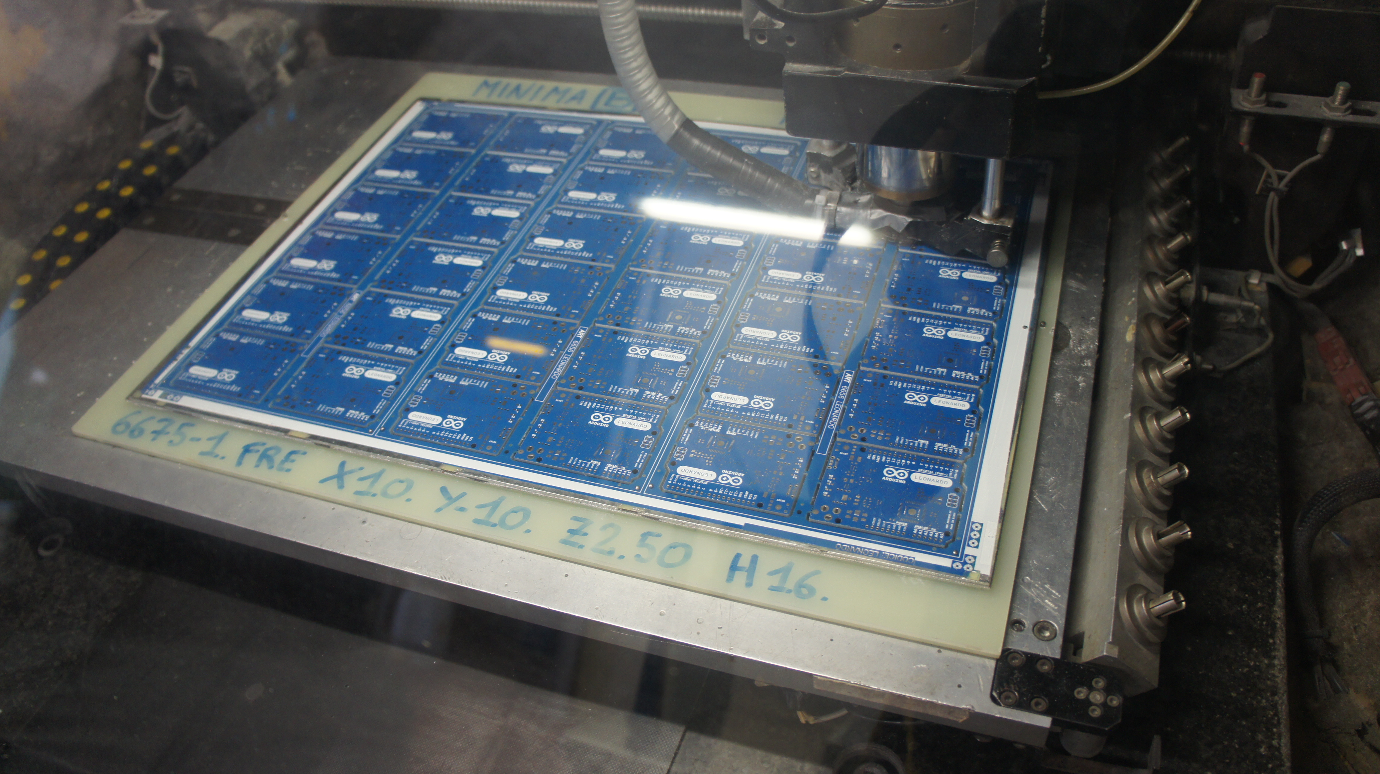
Before the boards can be shipped, the individual PCBs panels need to be routed so they can fit inside SMT machines. The boards are once again stacked up and batch-processed through a machine that uses a router bit to cut and release the board panels.

Finally, the boards are ready to ship on to the SMT facility. As you can see, the boards are panelized in a 2×6 format to make SMT processing more efficient.
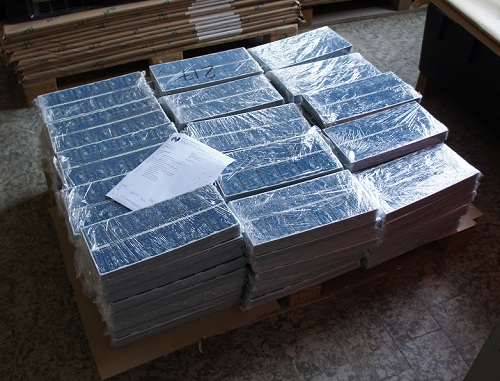
Here’s a veritable stack of about 25,000 bare Arduino PCBs ready to leave the PCB factory, moving on to be stuffed, shipped and sold to Makers the world around!
Many thanks to the Officine Arduino team and Davide Gomba in particular for taking time out of their busy schedules, showing me around, and patiently waiting as I expressed my inner shutterbug and general love for all things hardware…
HTML5 video <3! \o/
[…] Where Arduinos are Born: Touring a PCB Factory @ bunnie’s blog. Arduinos are made in Scarmagno, Italy, a small town near the Olivetti factories on the outskirts of Torino. All of the circuit board fabrication, board stuffing and distribution is handled out of that small town. I was really excited to see the factories, and I’d like to share some photos of them with you. The highlight of my tour was “System Electronica”, the PCB factory which makes the Arduino PCBs. […]
[…] Huang recently toured the Arduino production facilities and wrote a great post about what he saw (with lots of photos!): Arduinos are made in Scarmagno, Italy, a small town near the Olivetti […]
This is fascinating. Thanks for all the hi-res pics!
Is the SMT facility next? ;)
I’ll second this one! …great tour btw!
Hear hear! I’d love to see that.
Many of the photos, particularly of the lithographic processes, have a distinct yellow hue to them, is this just a white balance issue or is there a reason to use yellow lighting?
The rooms where board exposure and development happens are actually lit with a dim yellowish light to prevent accidental exposure to the photosensitive films. The camera automatically adjusts the aperture to take more light in the dim rooms, making them look brighter than they really are.
I guess it would’ve been awkward if you had forgotten to turn off your flash!
How does ferric chloride taste like?
I imagine a bit like FeCl matter.
“a bit like FeCl matter.”
Superb…. 5 stars!!!
Hi, many thanks for the reportage and the high resolutions pics ! ;)
[…] video below we can see how the flying probe test is performed on Arduino pcb’s. Credits go to bunnie for recording the video. We can clearly see that the step is the final step in the PCB fabrication […]
[…] Even if you’ve never designed your own circuit boards, and had your files magically turn into circuit boards, I’ll bet you’ve wondered what a circuit board factory looks like. It looks like this. […]
The dull white (maybe nickel) plating is what plates vias and PTHes and remains in the holes when the surfaces of the board are cleaned back to copper?
Copper is plated then Nickel on top of that, the Nickel acts as an etch resist when. The Nickel prevents the plated tracks and pads being etched away when the unwanted copper is, the nickel is then removed afterwards.
Actually the white dull colour plating is not nickel. It is Tin. The Tin layer is used to cover the surface from being etched which is will be used later for finishing. In this case is Hot air Leveling. After Stripping the dry film, it goes to etch, then to tin stripper. That’s why you will see back the copper. Nickel stripper is very expensive.
Nickel actually not dull, it is shining like chrome. Just for your information,
[…] Huang visited System Electronica, the PCB factory which makes Arduino PCBs, and the results of his tour are simply […]
[…] Arduino kretskortslaminaten (PCB) tillverkas i Italien och staden Scarmagno, här är ett bra reportage hur laminat tillverkas och i detta fallet Arduino Leonardo, detta reportage är inte unikt för Arduino utan principen är densamma för alla laminat som skall tillverkas. Mycket bra reportage med högupplösta bilder och filmer. Bunnies blog har gjort detta reportage. […]
[…] Hey look, an Arduino without its clothes on. This one’s just started its journey to becoming the ubiquitous prototyping tool. The image is from [Bunnie's] recent tour of the fab house where Arduino boards are made. […]
[…] All the pictures and movies can be seen at bunnie:studios. […]
[…] Hey look, an Arduino without its clothes on. This one’s just started its journey to becoming the ubiquitous prototyping tool. The image is from [Bunnie's] recent tour of the fab house where Arduino boards are made. […]
Hi Bunnie, I’m a long time follower, It’s nice to know that you are in Italy. I’d love to meet you and talk about a lot of stuff, so if you want to hang around with some fellow hackers, I’d like to invite you to our two hack camps here in Italy: the MOCA ( http://moca.olografix.org/moca2012 ) and the ESC ( http://www.endsummercamp.org/ ). The ESC is held just behind the Venice airport, so if you want to visit Venice that will be a good chance! :)
Hope to see you there! Let me know if you need anything!
Good work
[…] Detailed online factory tours are one of the best starting places to learn about manufacturing techniques. This tour of the Arduino factory provides a lot of information on how circuit boards are mass produced. (bunniestudios.com) […]
[…] Where Arduinos are Born [Link] […]
are you still in italy??
I lack the words to tell how much I envy you! :)) Still, it’s admirable you were so kind to share it with us. So in case I happen to ever get near Scarmagno, making a tour of the factory is a common option or you need to insist and eventually have some connections to step inside?
Nice report…
Thx
[…] el privilegio de poder visitar el lugar donde nacen los Arduinos. El tour que podemos ver en el blog Bunnie Studios es maravilloso, un recorrido por una fabrica de PCBs que se encuentra en Scarmagno, […]
[…] Where Arduinos are Innate: Touring a PCB Shop Where Arduinos are Innate: Touring a PCB Establishment @ bunnie’s blog – connection Arduinos are made in Scarmagno, Italy, a tiny urban imminent the Olivetti […]
[…] Pod TYM adresem znajdziecie relację w fabryki obwodów drukowanych do Arduino – autor fajnie pokazał cały proces powstawania obwodów drukowanych, w procesie przemysłowym. Powiązane wpisy:Quadrocopter na jednej płytce PCBEkstremalnie mały konwerter USB-serial – home madeFritzing – prosty autorouter Posted in Ciekawostki | Tagged Arduino, PCB, wytwarzanie obwodów drukowanych Share this post, let the world know […]
[…] Como fabricar un Arduino desde “0″ (link) […]
very cool, I love to get my hands on a Leonardo Arduino soon
beni
[…] http://www.bunniestudios.com/blog/?p=2407 Share this:TwitterFacebook Esta entrada fue publicada en NUEVAS TECNOLOGIAS. Guarda el enlace permanente. […]
Hey, how did u contact the factory officials for the tour? I could not find any contacts of the factory people.. I am going to Italy next week and would not want to miss a trip to the Arduino Factory.
Let me know as soon as you can!
Thnx!
system elettronica via Azario 48 STRAMBINO (TORINO) tel. 011-637388
info@systemelettronica.it
RCY PCB is a professional pcb manufacturer, we want to establish win-win relationship with you if possible
I’m not sure where you’re getting your info, but good topic.
I needs to spend some time learning more or understanding more.
Thanks for fantastic info I was looking for this information for
my mission.
Hey, I discovered your internet site by using Yahoo while looking for an equivalent topic, your website came way up, it seems like excellent. We have bookmarked so that you can favorites|included in this social bookmarks.
We’re heading to try to fix the mailing address/billing address thing.
Any requirements of PCBs,Please send your files to Andrew749@japcbpcba.com,we will make some free prototypes for some designer who pay attention to us.