First, I want to say wow! I did not expect such a response to this book. When preparing for the crowdfunding campaign, I modeled several scenarios, and none of them predicted an outcome like this.
The Internet has provided fairly positive feedback on the cover of the book. I’m genuinely flattered that people like how it turned out. There’s actually an interesting story behind the origins of the book cover, which is the topic of this post.
It starts with part of a blog post series I did a while back, “The Factory Floor, Part 3 of 4: Industrial Design for Startups”. In that post, I outline a methodology for factory-aware design, and I applied these methods when designing my book cover. In particular, step 3 & 4 read:
3. Visit the facility, and take note of what is actually running down the production lines. … Practice makes perfect, and from the operators to the engineers they will do a better job of executing things they are doing on a daily basis than reaching deep and exercising an arcane capability.
4. Re-evaluate the design based on a new understanding of what’s possible, and iterate.
My original cover design was going to be fairly conventional – your typical cardboard laminated in four color printing, or perhaps even a soft cover, and the illustration was to be done by the same fellow who did the cute bunny pictures that preface each chapter, Miran Lipovača.
But, as a matter of practicing what I preach, I made a visit to the printing factory to see what was running down its lines. They had all manners of processes going on in the factory, from spine stitching to die cutting and lamination.
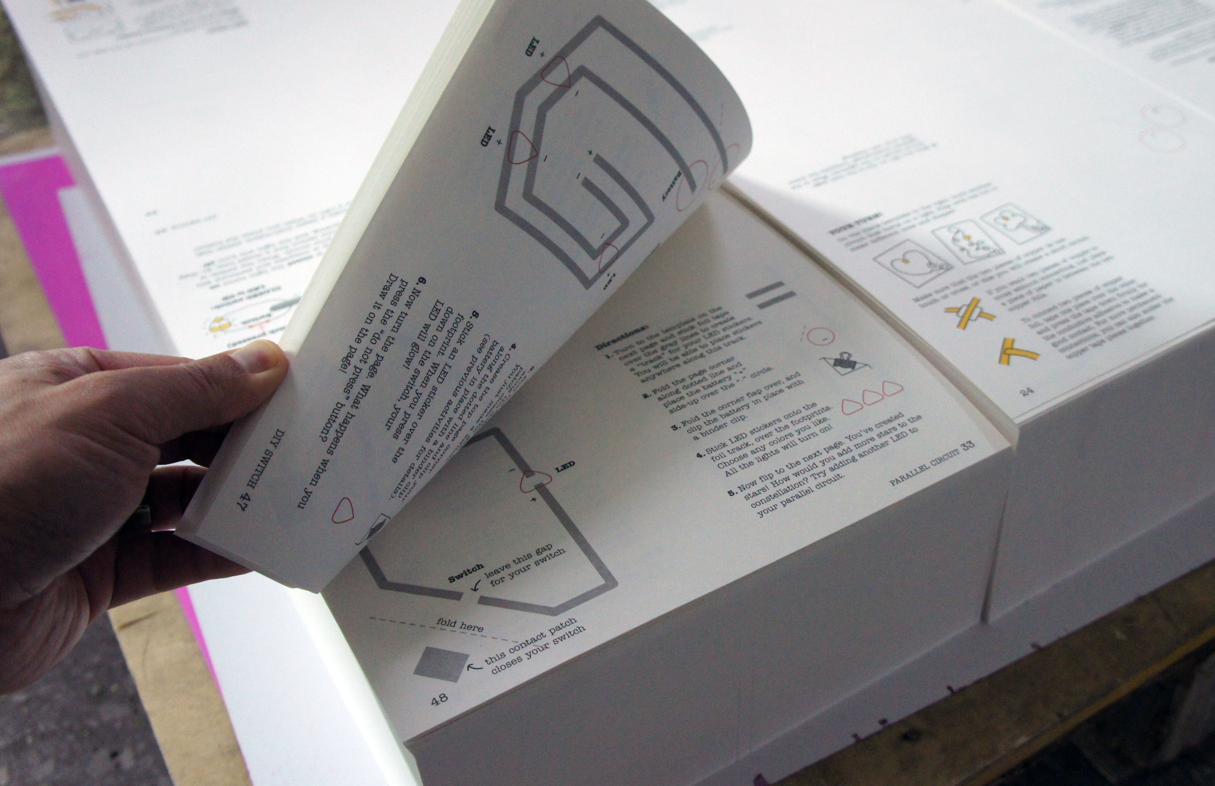
Chibitronics’ Circuit Sticker Sketchbook is also printed at this factory
One process in particular caught my eye – in the back, there was a room full of men using belt sanders with varying grits of sand paper to work the edges of books until they were silky smooth. Next to that was a hot foil transfer machine – through heat and pressure, it can apply a gold (or any other color) foil to the surface of paper. In this case, they were gilding the edges of books, in a style similar to that found on fancy bibles and prayer books. They could also use the same process to do a foil deboss on cardboard.
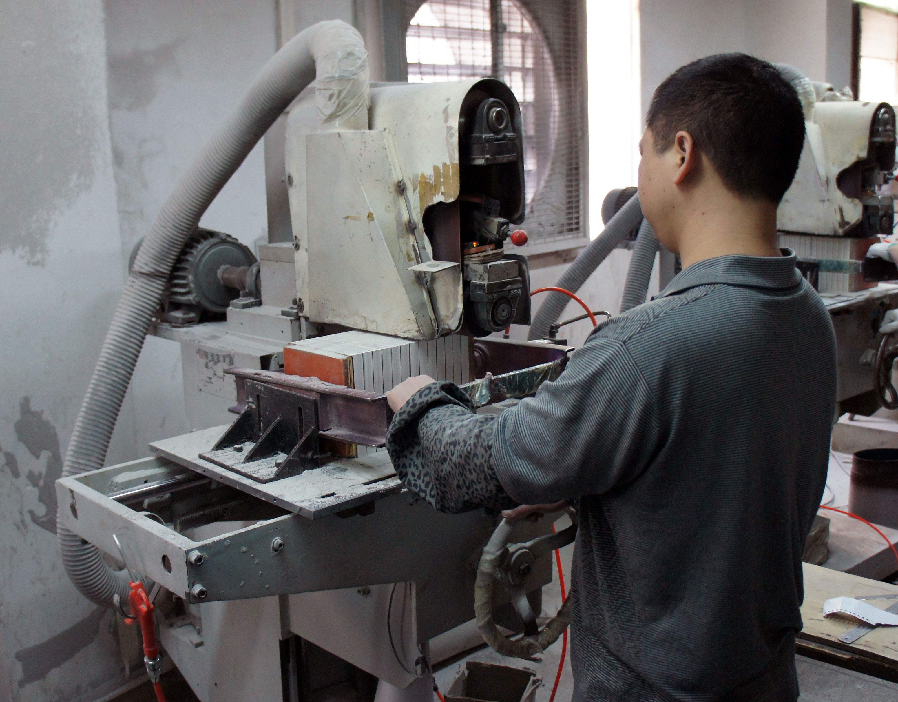
Beltsanding the edges of a stack of books until they are silky smooth
![]()
Closeup of the hot foil transfer mechanism
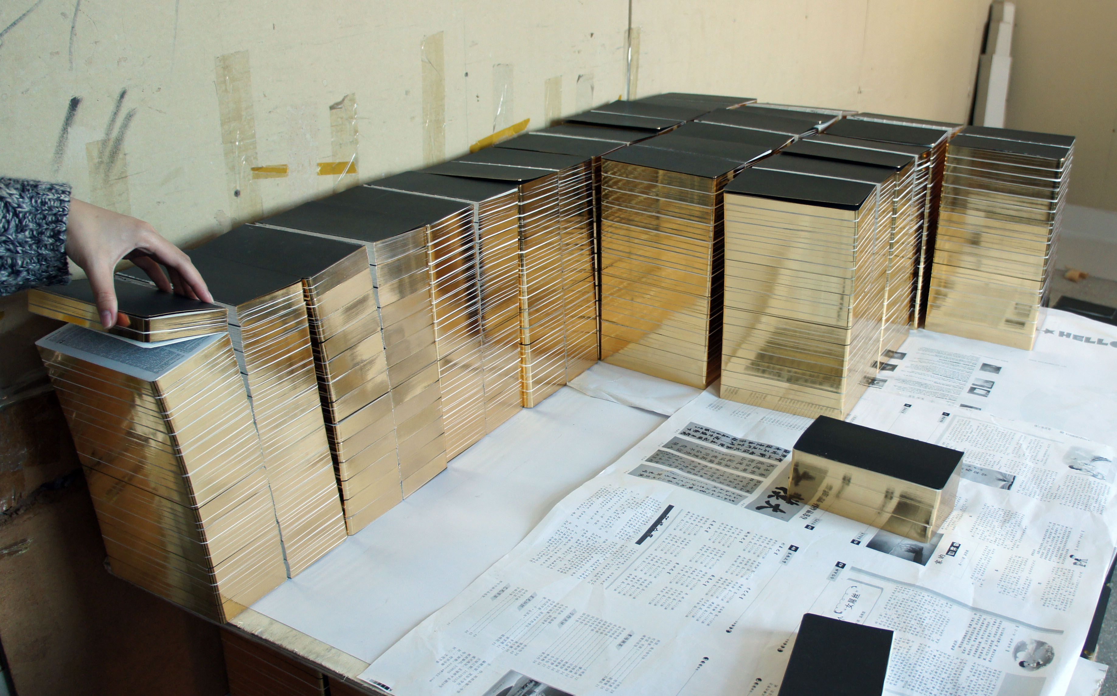
Stacks of books with gleaming, gilded edges
This is when I got the idea for the cover. These gilded books looked beautiful – and because the process is done in-house, I knew I could get it for a really good price. So, I went back to the drawing board and thought about what would look good using this process. The first idea was to take the bunny picture, and adapt it for the gold foil process. Unfortunately, the bunny illustrations relied heavily upon halftone grays, something which wouldn’t translate well into a gold foil process. Someone else suggested that perhaps I should do a map of China, with Shenzhen marked and some pictures of components around it. I didn’t like it for a number of reasons, the first one being the headache of securing the copyright to a decent map of China that was both geographically accurate and politically correct.
So I did a Google image search for “gold leaf covers” just to see what’s out there. The typical motif I observed was some kind of filigree, typically with at least left/right symmetry, if not also up/down symmetry.
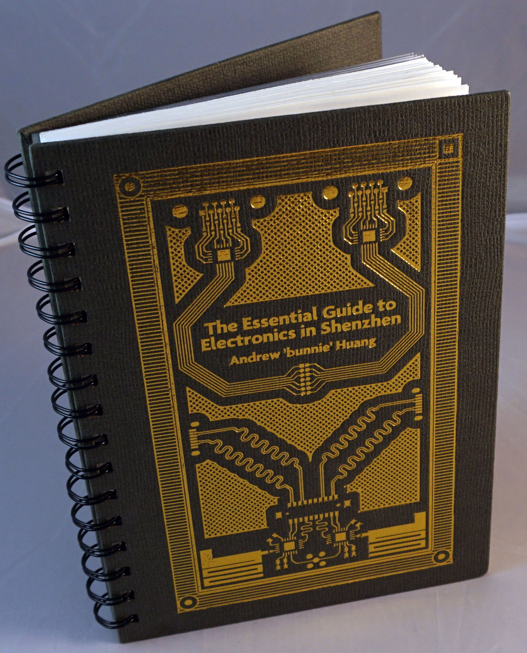
I thought maybe I’d go and fire up Adobe Illustrator and start sketching some filigree patterns, but quickly gave up on that idea – it was a lot of work, and I’m not entirely comfortable with that tool. Then it hit upon me that individual PCB layers have the same sort of intricacy as a filligree – and I live and breathe PCB design.
So, I started up my favorite PCB design package, Altium. I tried playing around a bit with the polygon fill function, using its hashing feature and adjusting the design rules to see if I couldn’t make a decent filigree with it. The effect seemed reasonable, especially when I used a fairly coarse fill and an additional design rule that caused polygon fills to keep a wide berth around any traces.
Then I had to come up with some circuitry to fill the cover. I looked at a few of my circuit boards, and in reality, few practical circuits had the extreme level of symmetry I was looking for. So I went ahead and cocked up a fake circuit on the fly. I made a QFN footprint based on fictional design rules that would look good, and sorted through my library of connector footprints for ones that had large enough pads to print reasonably well using the foil transfer process. I found a 2.4GHz antenna and some large-ish connectors.
I then decided upon a theme – generally, I wanted the book to go from RF on the bottom to digital on the top. So I started by drawing the outline of an A5 page, and putting a couple lines of symmetry down. In the lower left, I placed the 2.4 GHz antenna, and then coupled it to a QFN in a semi-realistic fashion, throwing a couple of capacitors in for effect. I added an SMA connector that spanned the central symmetry line, and then an HRS DF-11 connector footprint above it. I decided in the RF section I’d make extensive use of arcs in the routing, calling upon a motif quite common in RF design and visually distinct from digital routing. Next I added a SATA connector off to the middle edge, and routed a set of differential pairs to the TX/RX pads, to which I applied the trace length equalization feature of the PCB tool to make them wavy – just for added aesthetic effect.
Then I started from the top left and designed the digital section. Nothing says “old school digital” to me louder than a DB-9 connector (and yes, you pedants, it’s technically a DE-9, but in my heart it will always be a DB-9), so I plopped one of those down up top. I decided I’d spice things up a bit by throwing series termination resistors between the connector and a fake QFN IC; yes, in reality, not all pins would have these, but I thought it looked more aesthetic to put it on all the pins. Then, I routed signals from the QFN as a bus, this time using 45 degree angles, to a 14-pin JTAG connector which I placed in the heart of the book. Everything starts and ends with the JTAG connector these days, so why not?
The design now occupied just the left half of the board. I copied it, flipped it, and pasted it to create a perfect 2-fold symmetry around the vertical axis.
Around all of this, I put a border with fiducials and gutters, the same as you would find in a PCB destined for production in an automated SMT line. You’ll notice I break symmetry by making the top right fiducial a square, not a circle; this is a hallmark feature of fiducials, since their purpose is to both align the vision recognition systems and determine if the PCB has been loaded into the machine correctly.
Finally, I added the book title and author using Altium’s TrueType string facility, and ran an automated fill of the empty space to create the filigree.
I actually designed the whole cover while I was on the long flight from Hong Kong to Amsterdam for 32C3. I find that airplane flights are excellent for doing PCB routing and design work like this, free of any distractions from the Internet. As a bonus, every now and then someone comes along and feeds you and tops up your glass of wine, allowing your creative streak to be unbroken by concerns about hunger or sobriety.

When viewed in black and white, the book cover honestly looks a little “meh” – when I first saw it, I was thought, “well, at least maybe the geeks will appreciate it”. But after seeing the faux-linen with gold foil transfer sample, I knew this was the design I would run with for production.
The next difficult challenge was to not paint legs on the metaphorical snake. As an engineer, I disliked how over-simplified the design was. There really should be bypass capacitors around the digital components. And SATA requires series DC blocking caps. But I had to let all that go, set it aside, and stop looking at it as a design, and let it live its own life as the cover of a book.
And so there you have it – the story behind perhaps the only book cover designed using Altium (if you have a gerber viewer, you can check out the gerber files). The design went from a .PcbDoc file, to a .DXF, to .AI, and finally placed in a .INDD – not your typical progression of file formats, but in the end, it was fun and worthwhile figuring it all out.
Thanks again to everyone who helped promote and fund my book. I’m really excited to get started on the print run. The problem I’m facing now is I don’t know how many to print. Originally, I was fairly certain no matter what, I would just barely hit the minimum order quantity (MOQ) of 1,000 books. Now that the campaign has blown past that, I have to wait until the campaign finishes in 23 days before I know what to put on the purchase order to the manufacturer. And, shameless plug – if you’re interested in the book, it’s $5 cheaper if you back during the campaign, so consider getting your order in before the prices go up.
Tags: essential-guide
You should post a populated version of the board for the April NTW. Then you’ll find out what the circuit does.
thanks – I’m looking forward to building it (probablt with epoxy I guess … unless it’s real gold)
Interesting seeing what a difference the gold colour makes, the original B&W looks like it should be on the flyleaf of a Don Lancaster book from the 1970s while the gold version looks really impressive, a bit like M.A.R. Barker’s “Book of Ebon Bindings”.
Naise!! Glad to see you’re up to your creative self again. Gotta grab one copy of that + autograph for keeps!
Looks like stylised breasts and ovaries? Or is that just me?