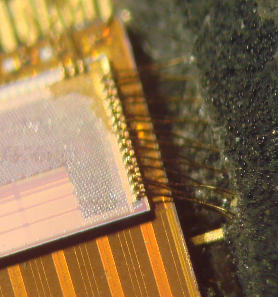
The Ware for January 2010 is shown below.
Is it really already 2010? Yikes. Almost 5 years running now with Name That Ware. Maybe I should make a nice color pin-up calendar of select wares for next year.
This is, of course, just a selected corner of the whole ware. I’ll give a hint: unlike last month’s ware, this is a very common ware.
[Added 1/27/10]
Looks like maybe I didn’t give enough hints. Here’s a couple more:
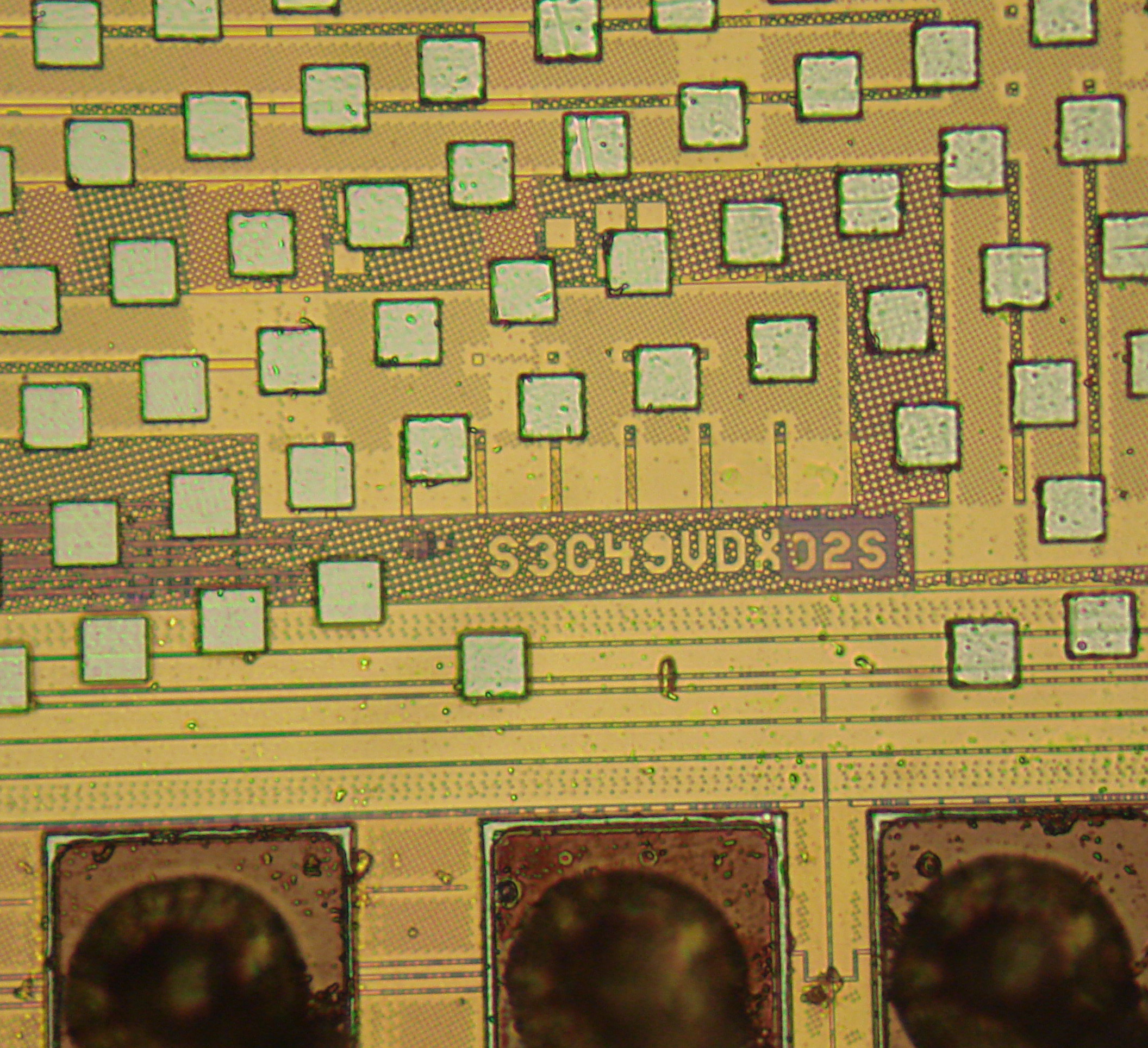
Above is a shot of the die marking on the top chip (S3C49VDX-02S). The bond pads at the bottom give you a sense of scale (click on the photo for a much larger version).
Some other thoughts and observations:
Looks like… a lot of things. I’m no expert, but to me it looks like the point where the silicon die meets the plastic casing of the IC, and the wires branch out to pins.
Maybe a calculator processor?
Or a CMOS/CCD sensor from a camera.
The part of the circuit that’s completely visible looks pretty regular in comparison to the stuff that’s under the dots. Maybe the cache or onboard memory for a processor?
Not enough pins to be an FPGA chip or a high-powered processor, so it might be a microcontroller.
As an added wild guess, the out-of-focus stuff at the top, as well as the off-kilter series of dots makes me think of a sense mesh, so I’m going to guess that this is a secure micro like the ones the fellows over at Flylogic spend their time breaking into.
Looks more like a chip stack – CPU (or in this case, probably flash) underneath, RAM on top. I am wondering about those dots; my only guess would be solder bumping.
As for which product it is, I’m stumped.
Don’t have a clue about the ware, but I Love the idea of the calendar. It’s a bit late for 2010, but maybe a wares calendar for 2011. I would buy one.
Having one would leave my workmate stumped with his nude calendar. Erotica is so mundane, but pictures of exotic hardware, now thats something!
The orange material that the die appears to be mounted on looks to me like a ribbon cable. Could this be part of an LCD module? The external interface would be on the ribbon cable itself, and the die would be mounted directly on top in order to keep it thin.
Oh, and maybe the dots are some sort of residue from an anisotropic conductive tape? That seems to fit my LCD theory, although I’m not entirely convinced that the scale of the dots (relative to the wire bonds for reference) makes this a reasonable guess.
broken iPhone?
Er.. I meant flex cable.
A _billion_ transistors? It’s got to be part of a memory/storage module. Maybe a flash chip?
Maybe the top chip is thick because it’s a stack of dies for higher density? Maybe the weird dot things are some sort of vertical interconnect? I’m not having very much luck finding convincing pictures of how this might work…
Smart card with 32 bit Samsung microcontroller.
128 KiB ROM, first rev, COB (obviously)
The squares in the second photo may be anti-tamper related.
1M transistors, not 1B.
If it really has 1B transistor, maybe secure USB flash drive.
Secure flash drive is not common, so maybe MP3 player or cell phone. Seems unlikely with so few bond wires.
The number of bond wires suggest an LCD or eInk display or maybe an RF chip (not shown).
Hm. Wasn’t solder bumping then! The size should’ve been obvious enough given the bond wires, true.
Dots are probably ye olde “oh my don’t look at me!” (anti-rev. engineering) features; they don’t seem connected to anything, and is probably just fluff.
I’m still going to go with “chip stack”, obviously – and the thinness of the die lends itself to that conclusion. Taking a bit of a wild guess here, I’m going to say “Samsung CPU/flash stack”. Probably iPhone/iTouch-related (1G), as the 3G seems to have an external flash chip; I do wonder where the DRAM went, though. Maybe this is a three-chip stack?
Also, you really wouldn’t have several billion transistors in anything but a large flash chip – well, unless it’s a huge amount of DRAM, which it probably isn’t given the likelihood of a CPU on-package (and it’s not 128 MB eDRAM as that uses 1T cells); I’d guess it’s a four-gig flash die. The signs of bonding wires in the background on the top image is also consistent with flash memory (dense covering of bonding wires on one or two edges).
Definitely a Samsung part #
Based on other parts with similar prefixes, its some form of “controller” – I’m guessing its a display controller of some form. (LCD screen)
At first, I looked at the orthogonal lead wires and traces in the bottom die and was reminded of a capacively coupled readout mechanism, but I’d bet real money that this isn’t a mosaic target imaging tube.
I’m guessing some sort of stacked dice System-in-package sort ot arrangement. This fits with something mass market (we’re told it’s a common ware) that wants to use latest technology without too much cost or lead time. Some sort of smartphone/PDA would fit nicely. Given that, I’m guessing the bottom traces are actually a flex PCB, common in space-constrained designs like phones.
Peering at it some more, I can’t help but notice the apparent anti-reverse-engineering overlay and the patterns on the top die. They aren’t regular enough for a camera CCD or memory array. So I’m thinking something else, which would also work very well with the flex circuit underneath: an ink cartridge monitor! The chip could use the horizontal stripes to capacitively monitor the ink level, and there may be some flash/EEPROM on board to remember time of use and ink flow, to avoid refillers resetting it. Since there is big money in selling ink cartridges, the makers are motivated to make hard-to-reverse chips. That also neatly explains the clear area without the anti-reverse pattern, as it would just be the capacitive level sensors which don’t contain much engineering, and would work best if unobstructed.
MLC Flash. A billion transistors + thick die leads me to MLC flash. The rest is the controller chip.
@John: A billion transistors seems excessive for an ink cartridge. It seems excessive for anything but flash memory.
Well, according to the Samsung Microcontroller Part number decode sheet :)
S3C49VDX-02S decodes as:
S3 = Microcontroller,
C = Mask ROM
4 = 32 32-bit
9V = Speical (IC Card) serial V
D = 128Kbyte ROM
X = Version 1
02S = Can’t decode this, but think its Wafer package.
You say ‘the top package’ which suggests its a stack, and the billion transistors can only really be flash. I assume from the odd stack thats its a smart card, no bonds down the connector edge?
Part of a Samsung LCD television?
Based on the large number of transistors I’m inclined to think flash memory. The use of a die stack like this makes me think its either some type of memory card, maybe microsd, or one of those tiny flash drives, like
http://www.transcendusa.com/Products/ModDetail.asp?ModNo=181&LangNo=0&Func1No=1&Func2No=76
Given stacked and high transistor count I’d guess a flash stack from a (micro) SD card.
Given the number of bond wires (if I’m seeing that right and they’re not inter chip bonds)) I’d think it is a (smart/feature)phone CPU/memory stack. Phones are bigger than SD cards, but space savings still count.
Smart CARDS do not have gigabits of memory, as far as I know.
just to be different, I’ll guess some kind of specialty chip for game cartridges… maybe the nintendo DS based on the hints about high transistor count…
I first thought this is a CMOS/CCD image sensor, but then there should be open window, instead of the epoxy being etched away. The square dots in second photo looks like dummy fill patterns just to fulfil the density rule of that metal layer, rather than anti-reverse-engineering measure.
The middle one should be another die rather than flex circuit. I think it’s more common to flip chip on flex circuit, rather than wire bond.
Richard’s find on Samsung part no decode confirms it’s a microcontroller. S3C49VA/B/C could be locate on samsung’s web site, but not the D variant. The part no and the thin die thickness suggest this is for IC card application. I guess it’s a SIM card or some RFID payment card that have space to store phone book or different vendors information.
GPU ! S3 Chrome ?!? :)
Hello, beautiful site. Thank you.
Based on the number of transistors, small number of i/o pins and the apparent physical size, I’m going to guess an SD card. Extrapolating the number of transistors, I’m going to be more specific and say a 512MB SD card.
The first picture looks like there are two dies staged on each other.
So I assume that its a Samsung ARM7TDMI based NAND flash controller below a 1GB NAND flash module.
http://www.datasheet4u.com/html/S/3/C/S3C49C9_SamsungSemiconductor.pdf.html
The square dots are maybe the remains of some kind of safety mesh with the top layer (made of alumium etc) etched away,like that:
—————————————————– Al layer
|| || || || sqare fields
Vcc vcc Vcc Vcc
Some of the square fields are leading into the chip to points which require Vcc or GND. The Al layer on top is set to either Vcc/GND.
As the Al is easily etched away with HNO3 when the chip is decapsulated, the chip is so rendered useless.b
Damn, the ASCII art drawing shall look like that:
————————————————— Al layer
——||———||———||——— ||—— sqare fields
—-Vcc—— vcc—— Vcc ——Vcc— layer which require Vcc/GND