Well, Chumby is finally shipping units in volume. You can’t go to the website yet and just buy one because we’re working through the long, long list of emails we received from people who asked to be notified when chumby devices are available for sale — there’s quite a backlog of orders there alone, although a few have shown up on ebay! I’m working on making some embedded developer (bare board) and craft (outerware only) units available for sale someday, separate from the consumer units. Hopefully that will make the core hardware more available to interested hackers and crafters.
The natural consequence of having many units out there is that we’re starting to see some interesting customer return cases. I recently got one unit that was destroyed due to an ESD (electrostatic discharge) event coming in from the power cord: the AMS1117 regulator that supplies the standby current for the CP and system management controller had been zapped. Interestingly, the unit worked for about an hour before it ceased operation.
This failure is particularly intriguing because there is a series of ESD protection devices between the AMS1117 and the power cord; at the front line, there is an AVX TransGuard transient voltage suppressor, then a set of EMI filters, diodes, fuses and so forth. Presumably, either some monster ESD event happened that not even these barriers could absorb, or the device was damaged on the factory floor prior to assembly. To investigate, I had the device decap’d and imaged by FlyLogic, and I found the results interesting enough to share.
Here is an overview of the damaged chip (click on the image for a much larger version).
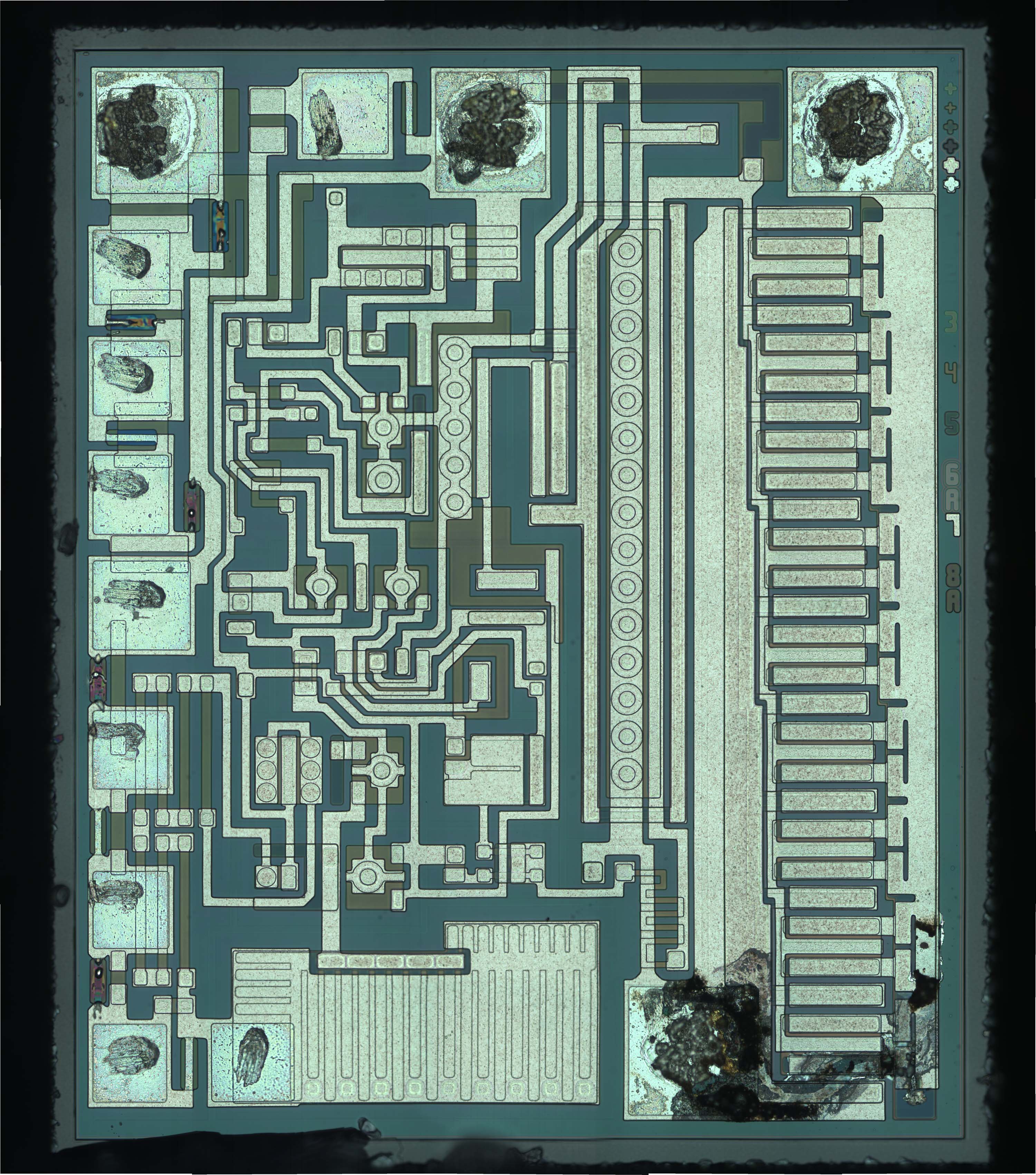
The spot with ESD damage is in the lower right hand corner, zoomed in here.

The path that the discharge event took between the output pin and the pass transistor of the regulator looks a little bit like a river channel that bends slightly up and over to the right. You can see how the metal was splattered and migrated by the ballistic motion of the electrons flowing by. This migration of metal eventually caused the pass transistor to get shorted out, so, unfortunately all the 3.3V devices downstream of this regulator got stuck with about 12V across them. Toasty! Fortunately, the PTC fuses on the board and other current-limiting mechanisms kicked in so the board never got dangerously hot.
One thing that struck me about this particular layout is the apparent lack of any on-chip ESD protection devices. Even though this is a big bad analog process, it seems non-intuitive to me that a bare device can stand up to the 2kV human body model tests that’s pretty much considered the minimum bar for ESD protection. Even if the device alone could stand up to the failure, it seems that what went wrong here was current arcing between two adjacent pieces of metal, possibly aggravated by the corona effect at the corners of the metal layout. At any rate, a device with no local ESD protection can be very susceptible, so perhaps even despite the precautions taken in the board layout, an external ESD event could blow up this chip.
I could be wrong, but perhaps I should now be looking for a chip vendor that was a little more fastidious about their ESD protection to prevent more unhappy customer return events. If any readers have some experience with analog chip processes like this, I’d appreciate a comment about the level of ESD protection you had to incorporate in your chip designs!
The ESD damage wasn’t the only interesting thing about the chip however. I also noticed burned out metal elsewhere on the chip:

There are several burned out spots like this on the left hand side of the chip.
This was a neat find, because this shows you how they trim these voltage regulators in the factory. For those not familiar with analog chip design, the accuracy of an integrated polysilicon resistor in an analog-optimized process is about +/- 20%. On a generic digital process, the accuracy is typically much worse (on the other hand, matching between devices on the same chip can be extremely tight and the quality of the match is proportional to the area of the device). Thus, when a chip advertises +/-1% accuracy for voltage, it has to have some kind of post-fabrication trimming mechanism built in.
Basically, the trim mechanism is constructed using a ladder of resistors in series, with shorting metal straps in parallel with each resistor. Therefore, when the chip is first manufactured, the calibration resistor ladder has a nominal resistance of nearly zero ohms. At wafer test, the chip’s output voltage is measured, and resistance is selectively added to this calibration ladder by using a series of high current is pulses to selectively blow the metal straps. Thus, the native chip design, without calibration, always shoots too far one way on the voltage, so you can always correct the problem by only adding resistance to a calibration ladder. If they did the design right, they would have it start with the voltage too low, so that if a fuse was only partially blown and it managed to repair itself (this does happen), you would only end up passing too little voltage to the regulated load, instead of too much — under the theory that if you are to have a malfunction, it’s typically safer to push less voltage than too much.
You can see all the extra bond pads used for this calibration process along the left hand side of the chip. There are very deep “scrub” marks, so large, heavily weighted needles were used to touch down on the wafer. This was probably necessary because of the high currents required to blow the metal fuses. Other trim mechanisms I’ve heard of include poly fuses, eFuses, or laser trimming, but I had never seen one “in real life” — they had always been an intellectual curiosity that I’ve read about in a process manual or a journal paper.
Wow, this post turned out long…
Wow. Bunnie, this post rocks. I’d like to think that I know quite a bit about hobbyist electronics and some computer engineering, but you continue to amaze me with the cool stuff you know.
I especially love the investigative process you went through in piecing together a specific failure case. I would absolutely love to be this customer and getting to read all about what happened after my busted Chumby’s death and return process.
I second that. Your series on manufacturing in China was one of the most interesting things I’ve read in a long time, and this post is right up there too.
Now I *have* to buy a Chumby just as a way of saying “thanks!” :-)
Releasing an “embedded developer bare board” would be sweet, the hardware is the best part. In case i missed something, will the board schematics / hardware info be posted? if so where?
You can find the schematics and hardware info for the boards at
http://www.chumby.com/developers/hardware
You might need to create an account on the website before the link works however — I’ve noticed that some links I post don’t work for people who aren’t registered on the website. In the case that you do have trouble getting to the link go to work, mouse over the developers menu bar, and then select “hardware”. There are links to all the docs about halfway down the page under the section titled “Release Hardware Version Code 0307 “Ironforge” — main board”.
Have fun!
The “not at all confidential” note on the bottom of the schematic diagrams is awesome. i registered without a hitch and the link works fine,
Thanks,
Hi Bunnie,
Chumby at Linuxdevices
http://www.linuxdevices.com/news/NS5718528026.html
Regards from Brazil
Long post, but an awesome one. :)
[…] Chip IC ESD failure – [Link] Tags: AMS1117, ESD Filed in Technology […]
Hello, Bunnie. I am a chumby owner, and I love it. Not a complete geek, but purty close. To the point where I am considering learning some coding finally (after all these years) just to make a widget. I will admit I am somewhat biased toward your efforts and talents, but you have done a wonderful job with this product. Cholly is so fun to use. Wish I didn’t have to unplug him to carry him around, but I can live with it. Someday, I am sure, we will have some alternate power source….
Your post has made me fearful of surges, but that’s life, too, right? In the meantime, what fun. The speakers are amazing. The ease of use, equally so. I love my Cholly. Can’t wait to cook tomorrow for Thanksgiving with Cholly by my side. Thanks, Bunnie!
any chance a hardware developer kit (barebones pcb) will become available?
-Dane
Hello Bunnie,
Your description is pretty much accurate with a few exceptions. The ESD damage you are referring to is actually EOS damage (Electrically Overstress). The ESD damage, in most cases it is not visible because ESD damage is very fine line that it inside the transistor junction between Emitter and Base junction or Emitter and Collector junction and in some cases both. Only using high magnification you could see ESD and it is a white fine line inside the green area (the silicon) crossing from one metal trace to another.
In this case if you look at the magnified picture you can see the bonding pad in the left is the Collector (device input for power pass transistor) and the melted metal as it trails to the right is the Emitter contact with the metal on the right side going straight up is connected to the output bonding pad. There are 18 Emitters connected to this metal trace to the upper right bonding pad (device output).
I do not know what is in the application circuit but it seems the case is high power surge damaged the device pass transistor. It has nothing to do with the power cord or the power supply used in the application but what happens when the power is turned on and what is connected to the regulator output. These devices have a maximum power dissipation that is determined by the die size (die area) and the package type. The power dissipation is the total energy the device can take without getting damaged. In linear regulators the total power dissipation is calculated by multiplying the voltage difference between input and output, with the load current flowing through the device pass transistor. In this case would be (12V-3.3V)* Io (Io is the output current). This would result in 8.7V multiplied by the output current. I do not know how much is the output current but from this you could find out how much power is dissipated on the device itself.
The die size determines how much heat can be transferred from the power transistor to the package lead frame. The bigger the die the more contact area is with the lead frame and more heat can transfer to the package lead frame. The package type also can determine how much heat can be transferred to the PCB and it has to do with how much area of the package is soldered on the PCB. The thickness of the lead frame could make some difference because if it is too thin the heat can’t irradiate sideways from the location where the die is attached and you end-up with a very hot spot under the die
Another thing could happen, and it is possible that’s what happen in this case, is the output capacitor. In most applications the output capacitor is a 10μF to 100μF aluminum capacitor. Aluminum capacitor is known to have high ESR therefore any voltage applied to it takes a few milliseconds to charge depending of the capacitor size. In cases where is a very large capacitor used on the regulator output or a very low ESR capacitor like ceramic (MLCC) is used, the instant current required to charge the capacitor is huge and may exceed the regulator pass transistor capability. Because most voltage regulators have a current limit protection circuit it will not supply more current than it is designed to supply and because of this the output voltage is pulled down to almost ground (0V) and slowly increases until the output capacitor is charged to the set output voltage. Going back to the power dissipation formula you can see what is happening here. In the first instant the output voltage is almost 0V, the output current is close to the device current limit trying to charge the output capacitor so the power dissipation is (12V-0V)*Io. Assuming the initial current required to charge the output capacitor is 800mA the power dissipation is 12V*0.8A=9.6Watt. Since this is enormous energy for such a small transistor does not even have time to heat-up the entire die but will immediately melt the shortest metal path creating a short across the Emitter-Collector of the pass transistor. If the energy would be gradually increased on the device the entire die would heat-up and the thermal protection circuit would shut-down the output by cutting the drive current from the pass transistor base.
Another exception in your description is in the metal fuses. In this circuit most of these fuses are to set the device fixed output voltages. For economic reasons you do not want to manufacture one design for each fixed output voltage but it can be programmed to the required voltage from the same design. In part you are correct; some of the fuses are for trimming the reference voltage accuracy. I do not know how much knowledge you have in trimming with fuses but with 4 fuses you could get less than +/-3mV error accuracy in the reference voltage. I hope this helps you for deeper understanding how LDO works.
Any chance the user just plugged in the wrong adapter (over voltage)?
What a relief to locate a blog post that’s finally really worth reading through! I’ve been seeking about about this topic yet folks just set trash posts, or small unreadable posts. I have viewed a couple vids on youtube but it is now the same as reading through a good article. Great job! Sorry for my crooked english.
hi there,
I’m working on a BTEC IT Student book for Pearson Educational Publishers in the UK and I was hoping that you would grant permission for us to use one of your ESD damage photos in the book, and also what credit line you would like please? If you could let me know by Monday 7th June, that would be much appreciated.
The book will be for WEL, excluding USA rights, and produced in both print and electronic form.
Many thanks
Maria