The Ware for September 2014 is shown below.
This months ware has a little bit of a story behind it, so I’ll give you this much about it to set up the story: it’s a USB protocol analyzer of some sort. Question is, what make and model?
Now for the story.
Name that ware is typically about things that cross my desk and get opened for one reason or the other — sometimes simply curiosity, sometimes more than that. This is a case where it was more than curiosity.
Turns out this analyzer broke at an inopportune moment. Xobs was working on a high-priority reverse engineering task that required some USB analysis. Unfortunately, when we plugged in the analyzer, it just reported a series of connect/disconnect events but no data. We initially suspected a driver issue, but after connecting the analyzer to a previously known good configuration, we suspected a hardware failure.
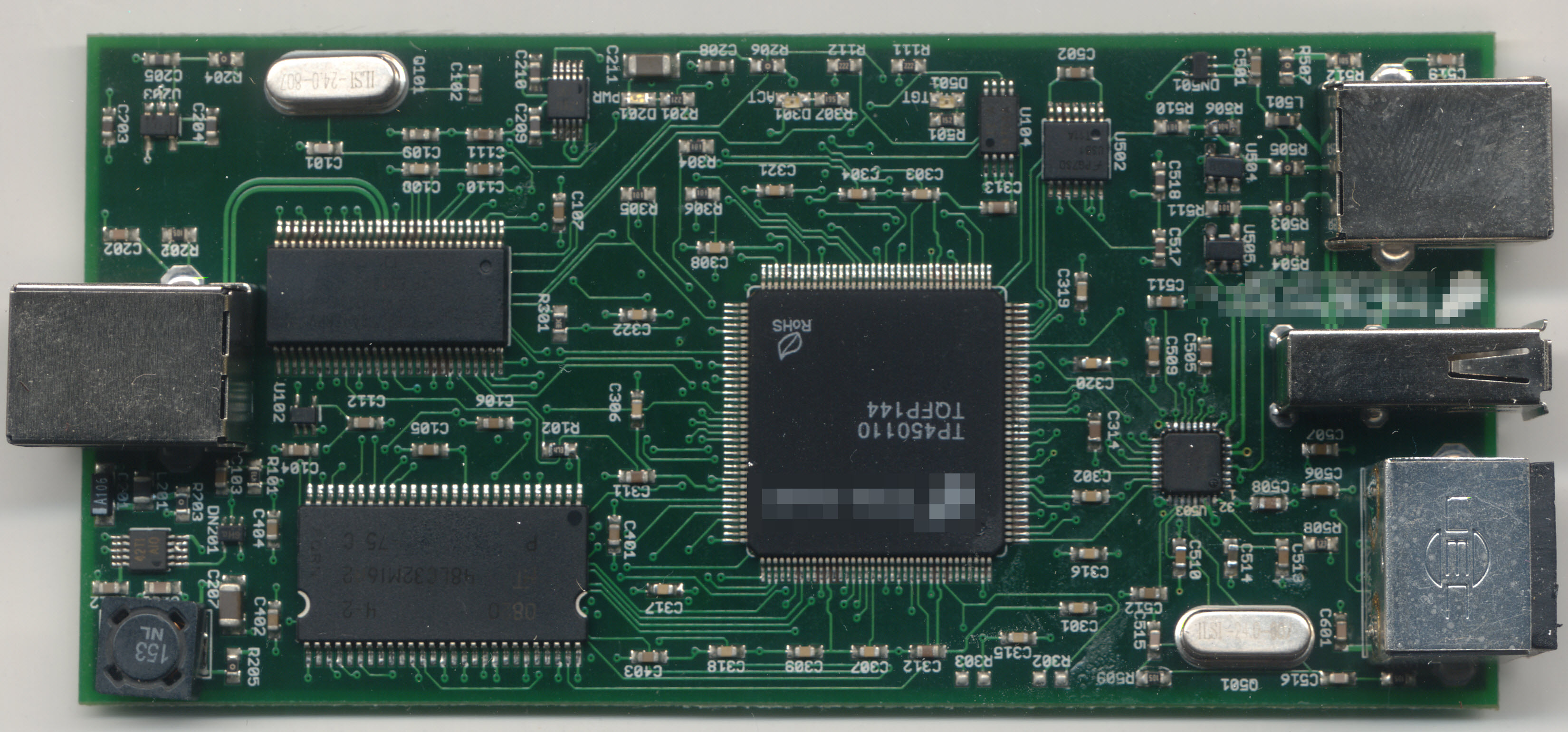
So, it was time to take the unit apart and figure out how to repair it. Of course, this is a closed-source device (still eagerly anticipating my OpenVizsla) so there are no schematics available. No worries; you’ll often hear me make the claim that it’s impossible to close hardware because you can just read a circuit board and figure out what’s going on. This particular ware was certainly amenable to that, as the construction is a four-layer board with a relatively simple assortment of chips on one side only.
The USB analysis front-end consists of three major types of chip, outlined below.

The chips in the red boxes are a pair of LMH6559 1.75GHz bandwidth amplifiers. Fortunately the top marking, “B05A”, was resolvable with a google search plus a few educated guesses as to the function of the chips. The chip in the yellow box is a Fairchild USB1T11A, a full-speed USB transceiver. And the chip in the green outline box is a Microchip (formerly SMSC) USB3300, a high-speed USB to ULPI transceiver. A casual read of the four-layer PCB indicates that the USB signal is passed through from the B-type port to the A-type port, with the LMH6559 acting as buffers to reduce loading, plus a resistor network of some type to isolate the USB1T11A. We figured that the most likely cause of the issue was electrical overstress on the LMH6559’s, since they lay naked to the USB port and quite possibly we could have shorted the data wires to a high voltage at some point in time, thereby damaging the buffers. We did a couple of quick tests and became semi-convinced that these were actually working just fine.
Most likely the issue wasn’t the USB1T11A; it’s well-isolated. So the next candidate was the USB3300. Fortunately these were in stock at Element14 in Singapore and just a few bucks each, so we could order at 4:30PM and have it delivered the next morning to our office for a very nominal delivery fee.
After replacing this chip, I was pleased to find that the unit came back alive again. I have to say, I’ve found the hot-air rework skills I learned at Dangerous Prototype’s hacker camp to be incredibly useful; this level of rework is now child’s play for me. I’m not quite sure how we damaged the USB3300 chip in the first place, but one possibility is that someone tried plugging something into the mini-DIN connector on the analyzer that wasn’t meant to be plugged into the device.
And so, despite this being a closed-source device, it ended up being repairable, although it would have been much more convenient and required a lot less guesswork to fix it had schematics been made available.
Significantly, the maker of this box was acutely aware of the fact that hardware is difficult to close and attempted to secure their IP by scrubbing the original markings off of the FPGA. An inspection under the microscope shows the surface texture of the top-part of the chip does not match the edges, a clear sign of reprocessing.
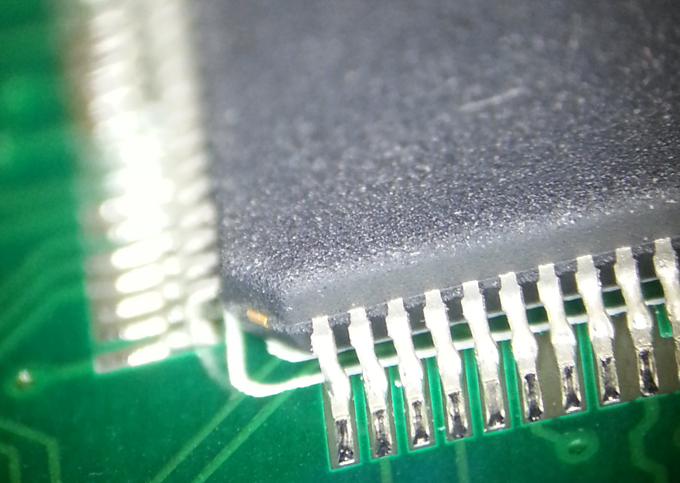
For what it’s worth, this is the sort of thing you develop an eye for when looking for fake chips, as often times they are remarked, but in this case the remarking was done as a security measure. The removal of the original manufacturer’s markings isn’t a huge impediment, though; if I cared enough, there are several ways I could try to guess what the chip was. Given the general age of the box, it’s probably either a Spartan 3 or a Cyclone II of some type. Based on these guesses, I could map out the power pin arrangement and run a cross-check against the datasheets of these parts, and see if there’s a match. Come to think of it, if someone actually does this for Name that Ware based on just these photos, I’ll declare them the winner over the person who only guesses the make and model of the analyzer. Or, I could just probe the SPI ROM connected to the FPGA and observe the bitstream, and probably figure out which architecture, part and density it was from there.
But wait, there’s more to the story!
It turns out the project was pretty urgent, and we didn’t want to wait until the next day for the spare parts to arrive. Fortunately, my Tek MDO4000B has the really useful ability to crunch through analog waveforms and apply various PHY-level rules to figure out what’s going on. So, on any given analog waveform, you can tell the scope to try rules for things like I2C, SPI, UART, USB, etc. and if there’s a match it will pull out the packets and give you a symbolic analysis of the waveform. Very handy for reverse engineering! Or, in this case, we hooked up D+ to channel 1 and D- to channel 2, and set the “bus” trace to USB full-speed, and voila — protocol analysis in a pinch.
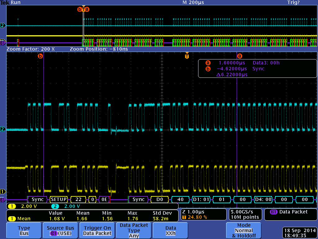
Above in a screenshot of what the analysis looks like. The top quarter of the UI is the entire capture buffer. The middle of the window is a 200x zoom of the top waveform, showing the analog representation of the D+ and D- lines as the cyan and yellow traces. And just below the yellow trace, you will see the “B1” trace which is the scope’s interpretation of the analog data as a USB packet, starting with a SYNC. Using this tool, we’re able to scroll left and right through the entire capture buffer and read out transactions and data. While this isn’t a practical way to capture huge swathes of data, it was more than enough for us to figure out at what point the system was having trouble, and we could move on with our work.
While the Tek scope’s analysis abilities made fixing our USB analyzer a moot point, I figured I’d at least get a “Name that Ware” post out of it.
Based on the layout of the ports and the blurred logo on the FPGA, it’s clearly a Totalphase Beagle. I believe it’s a Beagle USB 480, as I don’t see anything that looks like a current measurement shunt.
The original Beagle (usb 12) from total phase.
It is Beagle USB 480 Protocol Analyzer.
http://www.totalphase.com/products/beagle-usb480/
https://www.flickr.com/photos/eric_agan/sets/72157629595259368/
It look quite similar.
Is U102 the good, old CY7C68013 ?
Yes, it is. The markings show up MUCH better in the Flickr set Jakub posted, especially:
https://c4.staticflickr.com/8/7253/7140329925_4fecc335fb_h.jpg
I’m guessing the FPGA is an XC3S50A, since the datasheet says: “The XC3S50A FPGA is the only Spartan-3A device offered in the TQ144 package.”
Spartan 3A family is I/O optimized, but this application requires tons of logic, so if it’s a Spartan 3, then it should be Spartan 3E family IMO. XC3S100E and XC3S250E both come in TQFP144 packages but that would make PROG_B pin (or GND or TDO if they messed around with the pin 1 indicator during “securing”) connected to DATA0 pin of USB3300 which does not make any sense.
+ I also agree that it’s a Beagle USB 480.
Hi!
Very interesting, as always. For the FPGA, my quick guess would be a ProASICPLUS (APA075/100/300) or a ProASIC3e (A3P060/125) from Microsemi. The pinout seems to match and they have some embedded Flash memory.
this bog is very informative if we are looking and want to get details about USB protocol analyzer i like it