This post is part of a series about giving users a tangible reason to trust their hardware through my IRIS (Infra-Red, in-situ) technique for the non-destructive inspection of chips. Previously, I discussed the process of designing the IRIS light source in some detail, as well as my methodology for learning new things.
This post will describe the focus stage for IRIS.
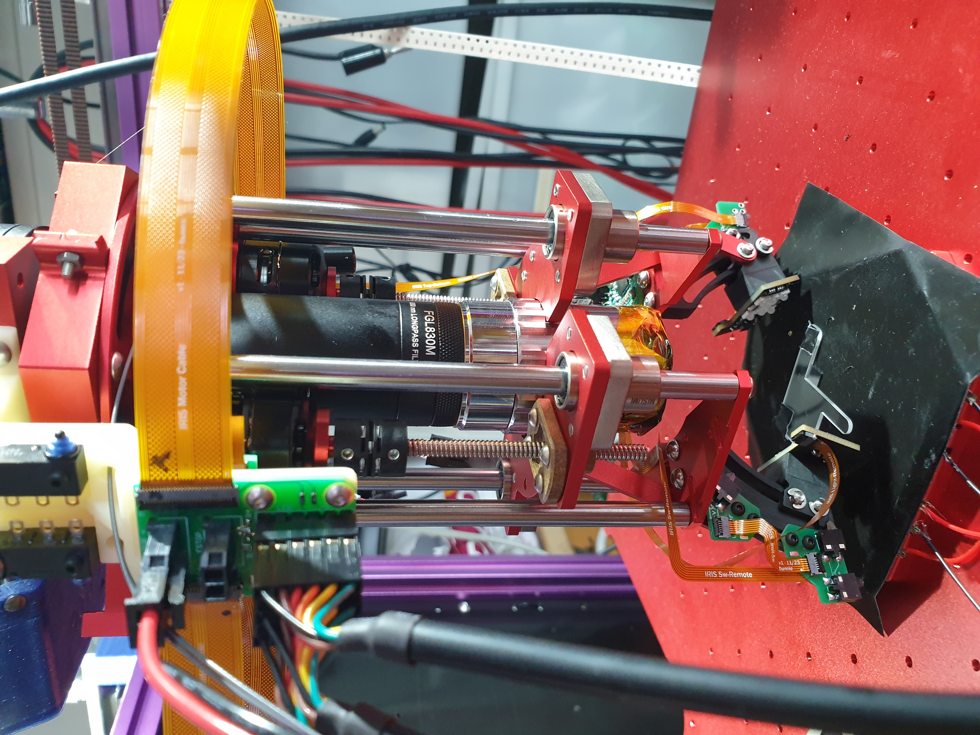
The focus stage is the thing at the bottom of the above image, covered in a black foil and with red and black wires coming out of one side. It’s responsible for controlling the fine positioning of the sample in the “Z” direction.
Background
The depth of field of the 10x objective used on IRIS is estimated to be around 8.5 microns. This means that I need to be able to control the distance of the chip to the lens in steps much finer than 8.5 microns. Note that depth of field typically decreases with increasing magnification, so if we want to support even higher magnifications, we would need even smaller focus steps.

Above: example of a calibration image used to measure the effective resolution of IRIS, which is about 4.75 pixels per micron with a 10x objective.
The resolution limit of the Z-stepper motors on the Jubilee motion platform is about 10 microns, so we can’t get our samples into perfect focus using the stepper motors of the motion platform alone (the Jubilee motion platform is the cage-like structure that the microscope is mounted in, you can read more about it here). One solution to this is to use an additional fine-focus mechanism that has a limited range of motion, but a very fine increment.
A bit of searching around reveals that a couple ways to do this include a micropositioner (basically a very fine mechanical screw-type mechanism) or a piezoelectric (piezo) positioner. I’ve never used a micropositioner or a piezoelectric actuator before, but the piezoelectric actuator seemed appealing because it would be a solid-state design – more compact, and less mechanical parts to machine and tune. The downsides of a piezoelectric system seems to be a limited range of motion, a limited amount of actuation force, and some non-linearities in position versus voltage due to hysteresis mechanisms.
Unfortunately, piezoelectric actuators are expensive. They start around $1000, and go up from there if you need features like kinematic coupling. So, I decided I’d try to build one from scratch, because it seemed like the rare case where solving an interesting problem with a one-off solution is also cheaper than buying an off-the-shelf unit.
After a couple of days scouring the Internet for suitable actuators, I came across the PowerHap (TM) series of piezo actuators made by TDK. They are intended for automotive haptic interfaces, and are available as a stock item at Digi-Key for around $20 in single unit quantities.
The larger actuators can produce a 100 micron deflection with a few Newtons of force. There are hysteric non-linearities, but they can be reduced with some preload and/or feedback mechanisms. Since the design is intended to be used with a dynamic auto-focus algorithm, absolute linearity is less important than monotonicity and repeatability (in other words, the non-linearities are probably not going to be an issue because we’re wrapping things in a feedback loop).
Sidebar: Kinematic Coupling
It would be convenient to be able to remove the fine focus stage to tweak a sample, and then place it back into the machine without affecting the repeatability of measurements. This would require a coupling that can mate to the stage with sub-micron accuracy with minimal effort. Simply shoving a plate onto a set of brackets or screw holes would not be able to achieve this level of precision. However, it turns out there is a well-established technique for accomplishing this: kinematic coupling.
I hadn’t heard of kinematic coupling until Prof. Nadya Peek, a collaborator on the IRIS project, advised me on the topic. The TL;DR is that in the most abstract sense, an object’s position in space can be precisely constrained with exactly six points of contact. Any less, and the object has a degree of freedom to move; but more importantly, any attempt to use more than six points means there is more than one stable solution for the position of the object.
Why does this matter? Because when systems are over-constrained, small imperfections in fabrication will cause extra constraints to fight with each other. You need to have a little bit of slop to ensure you can put things together without forcing parts together in ways that can damage them.
For example, I generally specify my screw holes to be at least 0.1mm, and ideally 0.2mm, larger than the screw meant to go through them. This makes it easier to assemble things, but it also means that every time I take things part and put them back together again, the final alignment of things moves around by about a hundred microns.
A hundred microns! That’s pretty big compared to the few-micron target of the focus stage.
It turns out that if you can reduce the coupling between the focus stage and its actuators to six points of contact, you can remove the stage and replace it repeatedly with a precision comparable to the size of the contact points. This is really desirable for being able to fiddle with samples without disrupting the work flow.
There’s some pretty good open-access material on how to design systems that are “exactly constrained”; this chapter from MIT’s 2.76 course and this thesis get into the meat-and bones of the topic.
However, the TL;DR is that the practical way to create an idealized “point of contact” is to push a sphere into a cylinder or a plane: for example, a ball bearing pushed onto a pair of dowels, or into a V-groove cut into a plate. If these are constructed from hard, smooth materials, you get pretty close to a perfect single point of contact. If you cut three V-grooves into a plate, and push three spherical bearings into the grooves, you’ve got six exact points of contact: a kinematic coupling!
The final piece missing is the force needed to make the system find its unique solution, i.e., the thing that pushes the spheres into the grooves. In the case of my microscope stage, the force comes from gravity acting on the top plate assembly, and nothing else.
Mechanical Design
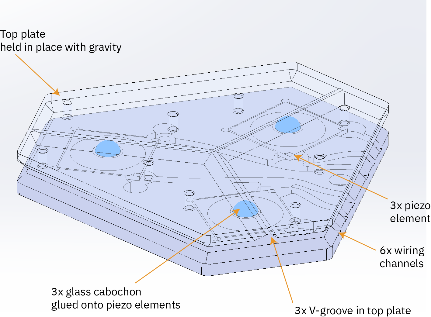
The idea behind the mechanical design is to keep it as simple as possible. The microscope stage itself is a simple slab of aluminum with three V-shaped grooves milled into it.
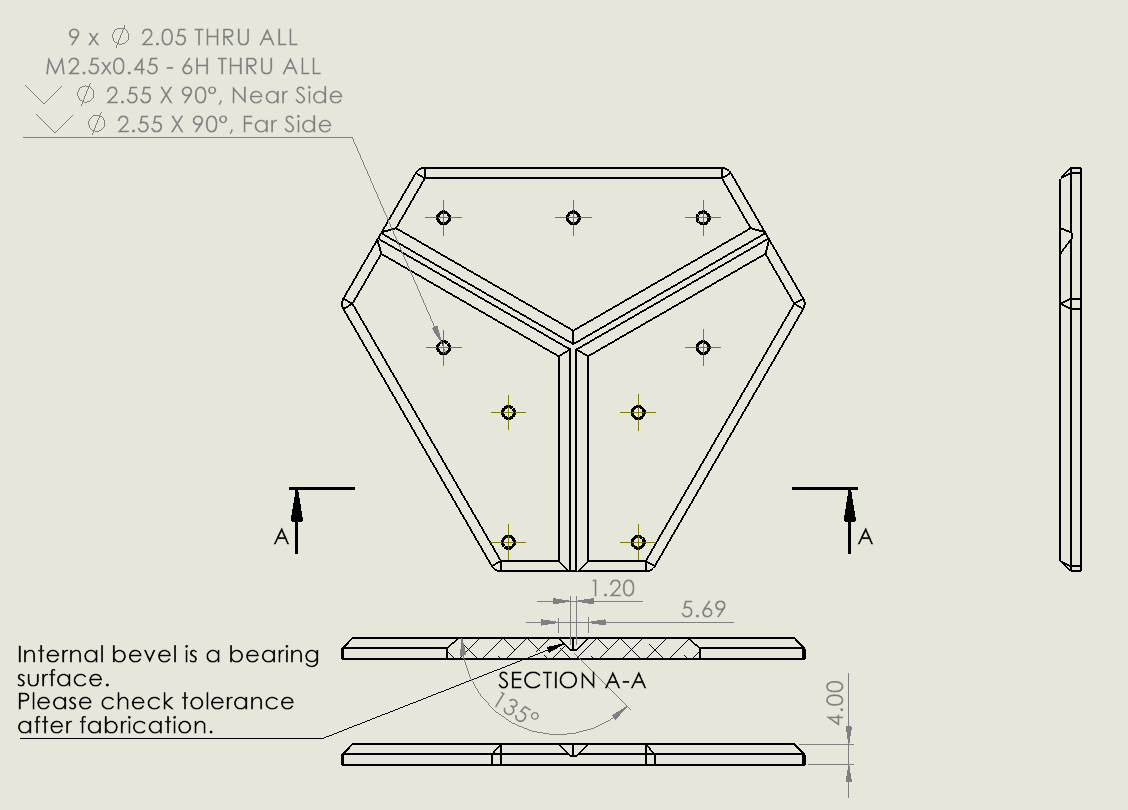
There’s a few holes drilled into the plate to help with mounting samples, but it’s about as simple as you can get. I’ll link to all the design files and where to order parts at the end of the post.
The piezoelectric actuators themselves have a simple shape:
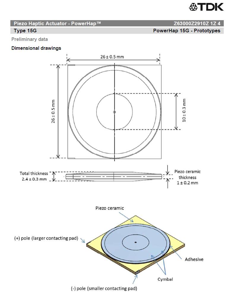
They are basically slabs of piezoelectric material with round “cymbals” bonded to either side. The cymbals act as mechanical amplifiers that increase the displacement of the actuator.
The center of each cymbal has a flat, circular region. I adhere a hemispherical glass cabochon to the center of the region using VHB tape to create the spherical half of the kinematic coupling. “Glass cabochon” (without affiliate code) sounds fancy but it’s a common and cheap material, often used in craft projects to add a bit of a sparkle or a dew-drop effect. The actuators themselves are mounted in an aluminum plate with channels to help route the wires to the edge.
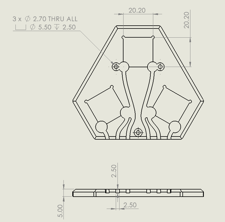
That’s basically it for the mechanical design – two aluminum plates, three piezo actuators, and three glass crafting beads with a bit of glue. “Kinematically coupled piezo actuated focus stage” sounds fancy, but one of the nice parts about kinematic coupling is that you don’t need to complicate them – you are trying to reduce a design to six points of contact, no more, no less.
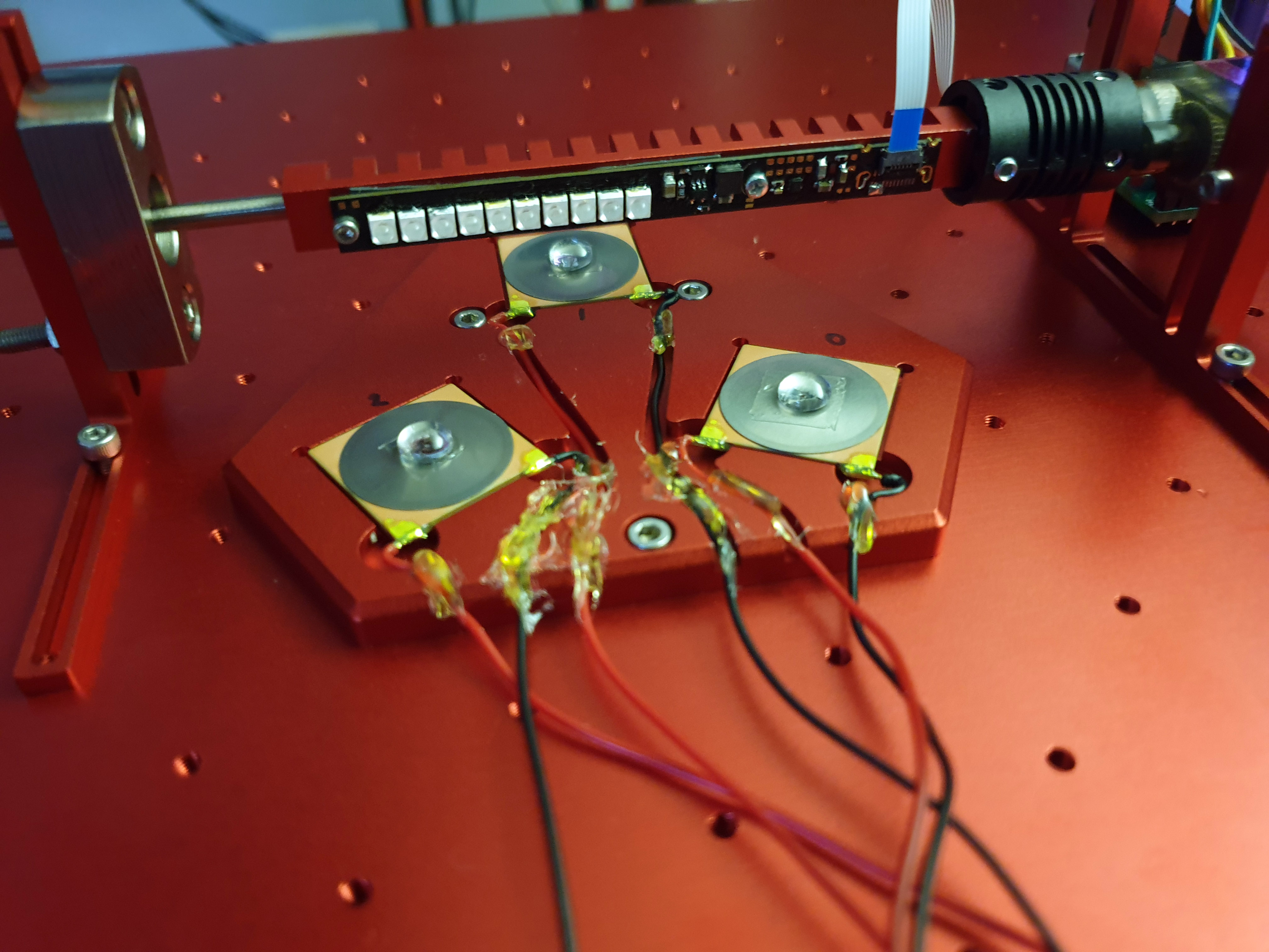
Above is a view of the bottom plate with the actuators and cabochons glued in place, but with the focus stage taken off.
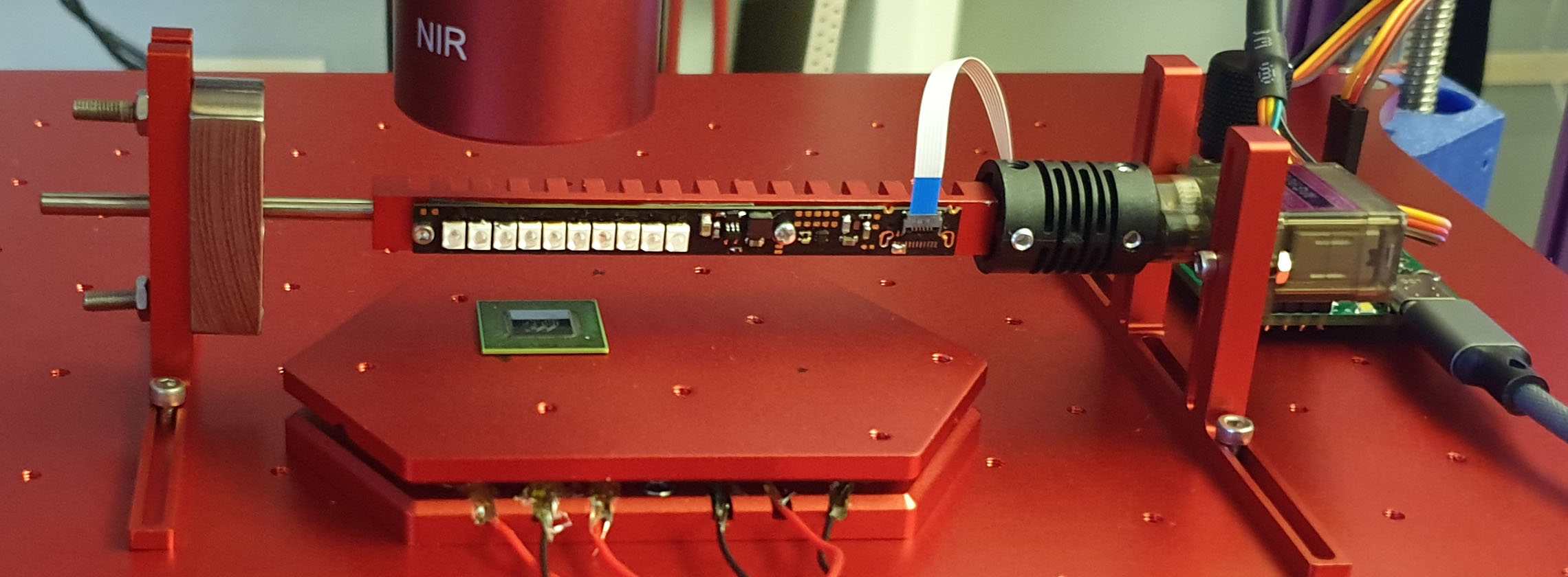
And above is the assembly with the focus stage resting on the cabochons. The only additions to the design that happened since the photos were taken is the addition of an Acktar black film to suppress stray light reflections, and a small L-shaped bracket to aid with squaring a chip relative to the microscope’s field of view.
An important additional benefit of using a kinematically coupled stage with three separate actuators for each pair of coupling points is that you also get the ability to trim the angle of the plane relative to the optics “for free” (the real cost is the headache of figuring out the maths to make it happen). As long as each of the actuators can be independently driven, you can trim the sample’s plane, thus keeping the entire region in focus.
Electronic Design
Conceptually, I wanted a Serial-to-Position widget: something that converts ASCII commands into different heights on the positioning stage.
I used an RP2040 with a small Rust program to convert serial commands into low voltages through a multi-channel, 14-bit DAC.
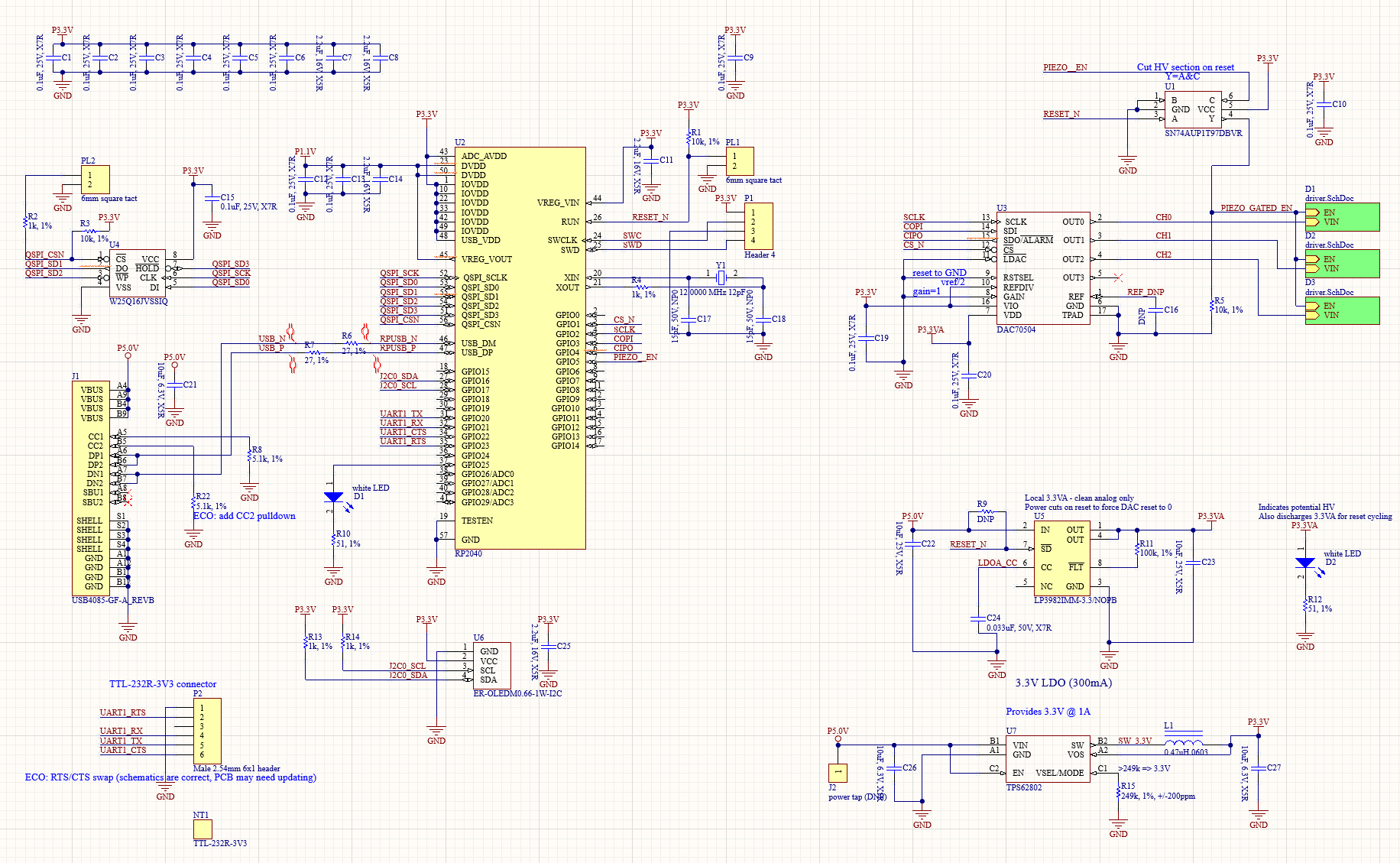
In theory, the 14-bit DAC could control the piezo position to a resolution of 6nm (100um stroke divided by 16384 steps), but I’m guessing the actual accuracy is closer to 10’s of nanometers because I was only modestly careful in isolating all the noise sources from the DAC. This is still plenty of resolution given that our target is to land within an 8 micron window. Unfortunately, I have no definitive way to characterize the absolute accuracy of the setup; a nanometer-precise laser interferometer capable of doing these types of measurements costs a mint, and are probably subject to strict export controls.
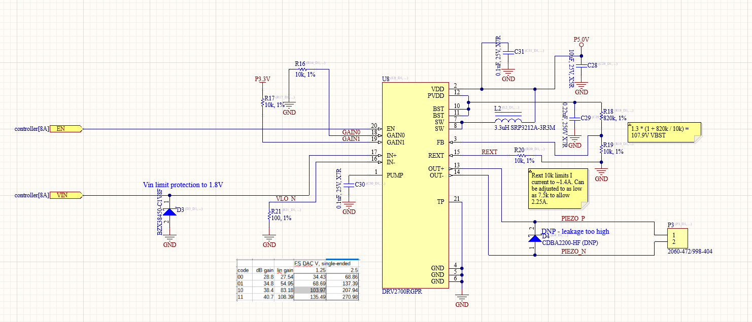
I then convert the low voltages into the hundreds of volts needed to drive the piezo actuators using a piezo driver chip. Thanks to the proliferation of haptic feedback interfaces in consumer electronics, I’m able to find several single-chip solutions for driving the actuators; for this design, I settled on the TI DRV2700. Since the DRV2700 is capable of higher voltages than I needed as well as negative voltages, the main challenge of the design was making sure I didn’t exceed the maximum specifications on the PowerHap piezo, and that I didn’t accidentally apply a negative voltage to it. This is compounded by the datasheet being a bit vague on some parameters, so I had to re-read it a couple of times and make some educated guesses.
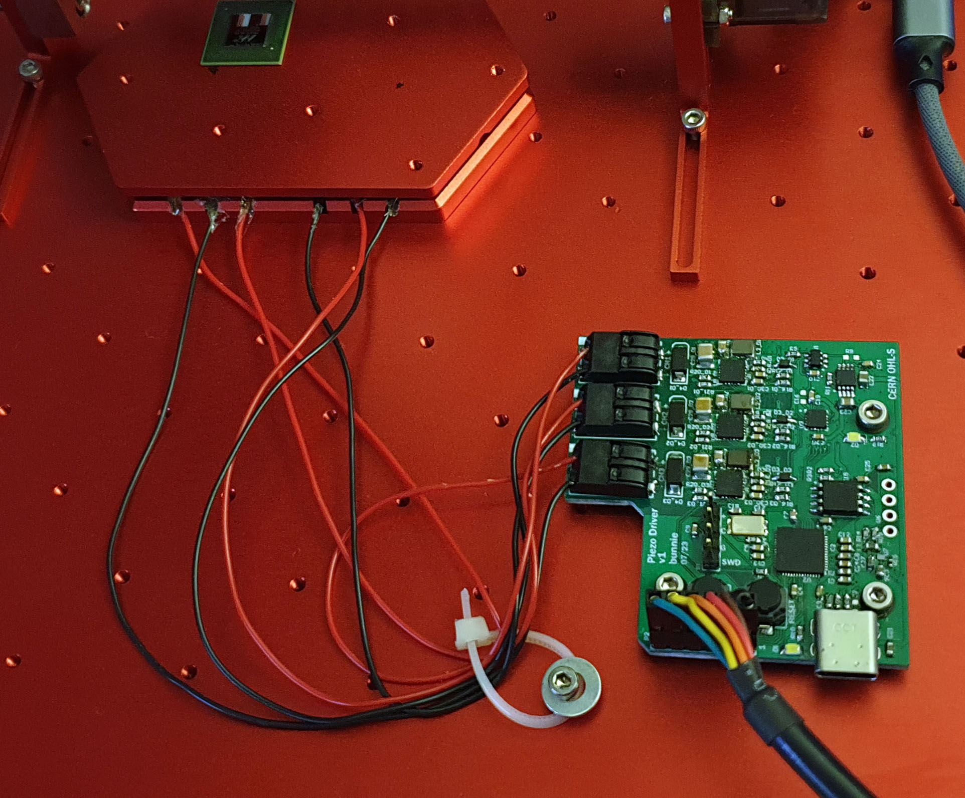
Above: hand-soldered, wired up and ready to go!
Testing high voltage drivers is always an exciting experience: the first time you command it to go to 100 volts, you sort of take a deep breath, close your eyes (so you don’t damage a cornea from flying fragments of chip package), and hit enter. While that test went smoothly, I did end up frying one channel during bring up so badly that the inductor desoldered itself from the board; this was also when I discovered that it was a bad idea to put reverse voltage protection diodes on the channels, because at high positive biases the leakage current was enough to cause the protection diode to self-heat, leading to higher leakage, leading to more heat … and eventually the circuit cooking itself off its pads.
However, once I got past the teething issues, things went surprisingly smoothly. The piezo actuator worked reliably and seems remarkably linear. Perhaps the biggest problem I encountered was that the response is too quick: the focus steps during auto-focus search were energetic enough that it would cause the chip samples to bounce around on the stage, causing them to “walk” out of the field of view over time. This was fixed with a small change in the control software to ramp the waveform, instead of doing a square-wave step to the final position.
Above is a short video of the auto-focus mechanism in action. The focus steps are very fine, so the effect is subtle. However, if you look at the bright laser marking stipples in the lower part of the image, you’ll notice more of an effect. In this video, the algorithm refocuses, sweeping the Z-height over a few microns, doing curve fitting, and determining the optimal point for focus on that step, all within a couple of seconds. The software algorithm to run the autofocus was actually much more challenging to get right than the hardware itself, and I’ll go into some of that in a future post.
The neat part is that at the end of the day, the whole thing cost a few hundred bucks, even counting all of the costs for one-off custom machining of parts and building circuit boards (it helps that I hand-soldered the whole thing myself). I’m not sure how this compares in performance to the thousand-dollar plus commercial alternatives, but it worked well enough and the software is tailored to exactly what I needed.
It helps that I can get CNC aluminum parts made at a reasonable quality for a very good price (about $55 for each of the aluminum plates) through a friend in Shenzhen. His company is called Jiada, and if you have Wechat, you can contact him at “Victor-Jiada”, and the design files can be found here. Just let him know that you got his contact via my blog.
Not a Product
The success of the design begs the question if I will offer it as a product. I’m not actually sure it would be worth it, because of creeping regulatory enshittification – FCC/CE certifications & declarations, RoHS, REACH, probably some UL/safety weirdness because of the high voltages, and unpredictable export controls because it’s related to semiconductor fabrication – is pretty significant, both in terms of real money cost but more importantly in terms of distraction, aggravation, and risk. Just last month, I had to write a letter to DigiKey explaining to them that no, really, I hand-solder everything in my home, and I’m not some fly-by-night trader re-exporting parts to banned entities like Russia or China.
I’ve also been burned by products bounced out of customs because of some small irregularity in the paperwork, followed up by angry customer emails about non-delivery, and ultimately me eating the cost of return shipping and a full refund to the customer, compounded with unsold inventory because my market shrinks with every new regulatory barrier – sometimes over really stupid stuff like post-Brexit UK requiring the words “UKCA” to be printed on products in order to pass customs.
Yes, I’m bitter, because I grew up in a world with fewer trade barriers, and without a DMCA. I remember when we were free to think, travel, and trade, and I liked it. I feel kind of sorry for the youth today, growing up in a world shaped by narratives of safety, fear, and ultimately, control. Also, climate change.

I digress.
Maybe if a few like-minded creators were interested in a kit of mostly assembled parts, I can make a “lo-fi” offering that skirts the most onerous regulations. But in the post trade-war economy, there is a disincentive to creating overly-polished products: if it looks too professional, regulators hold you to a higher level of scrutiny, and that makes it not worth the effort to “do better”, especially for small, bespoke lab tools like this. Welcome to the world of enshittified hardware.
Besides, I don’t have access to nanometer-precision metrology tools, so I’m not actually 100% sure what the piezo displacement curve looks like: “it works for IRIS”, and that’s about all I can guarantee.
DIY
The good news is that all this work is open source, so you’re more than welcome to build your own version of this nm-resolution piezo focus stage based on my design files – you should be able to find everything you need to do that at this github repository! You’re even free to sell product based on these files, but, don’t expect me to support your customers – my work comes with no warranty of fitness. You sell it, you support it!
The next post will dive into the mechanical design of the light positioner itself. Thanks for reading, and thanks again to NLnet and my Github Sponsors for supporting my research.

[…] 详情参考 […]
As the owner of a 2nd bedroom electronics business empire I hear you on the enshitification of trade :(
Thanks for the detailed write-ups! While I don’t need an IRIS microscope, a few of the parts and methods may become useful in other projects.
> Unfortunately, I have no definitive way to characterize the absolute accuracy of the setup; a nanometer-precise laser interferometer capable of doing these types of measurements costs a mint, and are probably subject to strict export controls.
On the contrary, interferometers are easily accessible and probably cheaper than you think.
* https://www.repairfaq.org/sam/manuals/hobspcl1.htm
* https://www.ebay.com/itm/303500535042
[…] Huang has steered that the main target stage is not going to be supplied as a product, however has included the design within the IRIS {hardware} repository underneath the Strongly Reciprocal variant of the CERN Open {Hardware} License Model 2. Extra data is obtainable on Huang’s weblog. […]
I think that at this stage of development, anyone who has a need for this capability should be building their own in order to integrate the principles involved.
Interesting project!
If you are looking for coarse and fine positioning in a single stage, you may want to consider Xeryon. Their products are driven by ultrasonic piezo motors, which offer the compactness and precision of piezo systems, but with much more travel range, speed and durability.
https://xeryon.com/products/