The Ware for August 2020 is shown below.
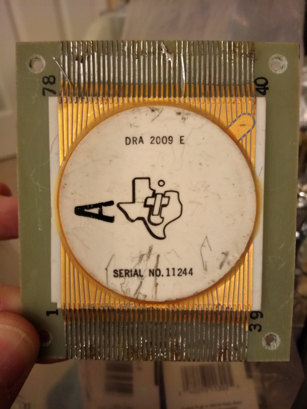
While sending me an unrelated photo that I will feature in a future Name that Ware, David Willmore nerd-sniped me with this incidental photo. It is as of yet unidentified, but as far as I could tell it’s from a short-lived family of 1969-era Texas Instruments “DRA” — a Discretionary Route Array. Basically a wafer-scale bipolar gate array (back when “wafer-scale” meant one 1.5″ wafer — hence the circular boss in the middle of the package), which could run at speeds of up to 10MHz. For example, the DRA-2003 was a dual 501-bit shift register, and cost $390 back then in 100-249 unit quantities (around $2,800 inflation-adjusted). As an interesting side note, the rule-of-thumb pricing for a single processed 12″ wafer today is … about $3,000. That’s Moore’s Law for you: 50 years got us roughly a billion times more transistors on a single wafer of 64x the area for about the same cost.
I couldn’t find anything on this specific part number (DRA-2009E), so I figured why not turn it over to Name that Ware to see if anyone could come up with more details, about the logic family itself, or ideally about the specific part number shown here.
I found references to a DRA-3008 test chip in this NASA report on Quality Standards for Bipolar LSI, https://ntrs.nasa.gov/citations/19700023200
And some cut away images of the package in this earlier report https://ntrs.nasa.gov/citations/19700023200
No mention of the DRA-2009E in any of the reports in that collection though unfortunately.
That is a spectacular find, well done.
Thanks!
I realised I pasted the same link twice. This is the correct link for the report that had results on testing the DRA-3008 https://ntrs.nasa.gov/citations/19710018295
The other reports in the collections can be found by searching for “NAS8-21319”
The Smithsonian chips collection also has a transcription of some TI marketing stuff mentioning DRAs in general, but also nothing about the 2009 – I’m guessing this is maybe where the original info was from, but still could be interesting for everyone else:
http://smithsonianchips.si.edu/ice/ICE_LSI_DRA1969_1970s11.pdf
(Linked from the top of this page: http://smithsonianchips.si.edu/ice/s11-100000.htm )
That NASA report was an interesting read, they seemed to use these sort of like modern flash memory, where they expected a certain number of defects per wafer and so would run an automated test to find which cells were bad, and have routing software create a unique metal-layer pattern to match the desired netlist while avoiding the bad cells.