The ware for June 2025 is shown below.
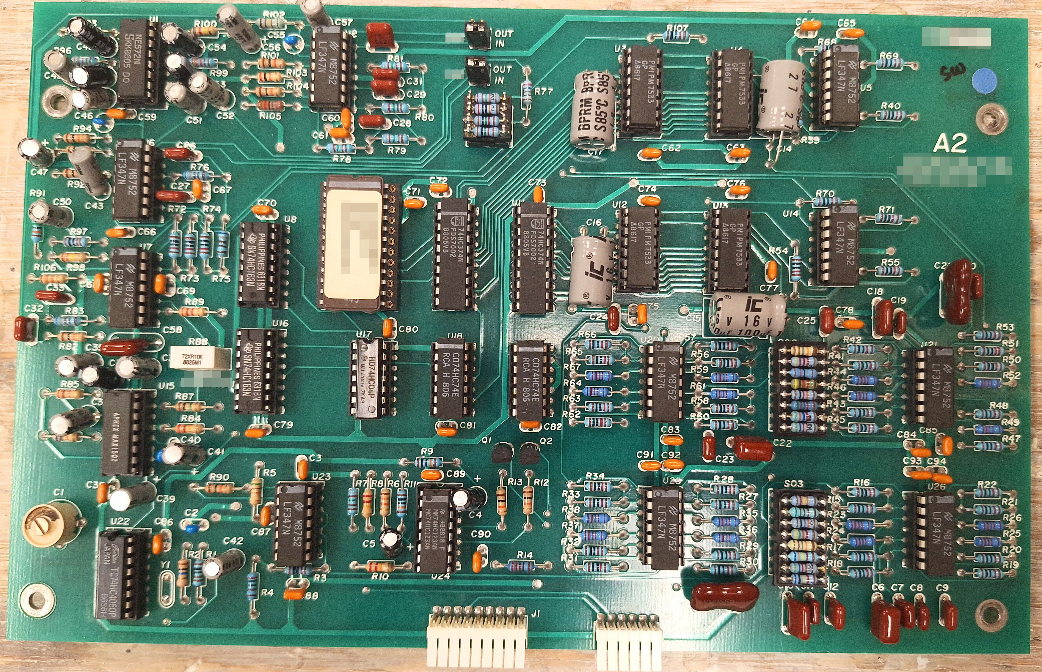
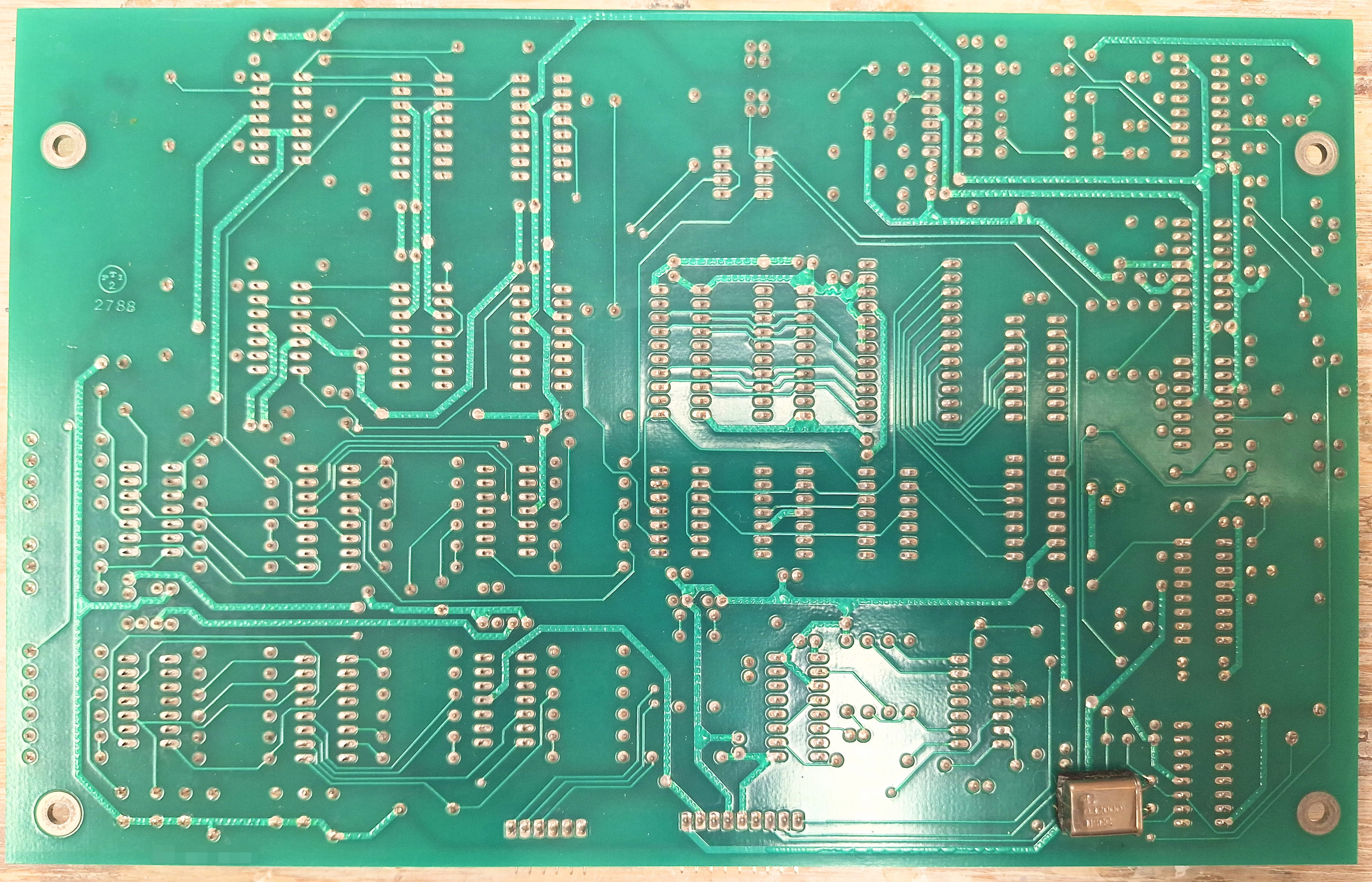
A big thanks to Chris Combs for this handsome contribution! Despite being 80’s vintage, the board is in mint condition.
The ware for June 2025 is shown below.
A big thanks to Chris Combs for this handsome contribution! Despite being 80’s vintage, the board is in mint condition.
The Ware for May 2025 is a Facebook (now Meta) Portal. I’ll give the prize to opticron for the quick guess, email me for your prize!
I actually considered redacting the audio DSP, but decided to leave it in because it’s an interesting detail. Despite having a big burly SoC with multiple cores and a GPU, the designers still opted to integrate a dedicated chip for audio DSP. I guess silicon has gotten cheap, and good software engineers have only gotten more expensive.
I’ll also give an honorable mention to Azeta for doing a great “spirit of the competition” analysis. Thanks for the contribution!
The Ware for May 2025 is shown below.
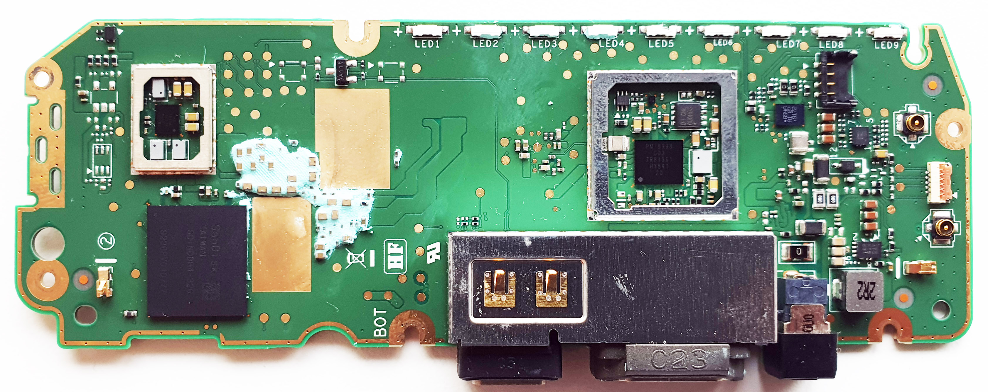
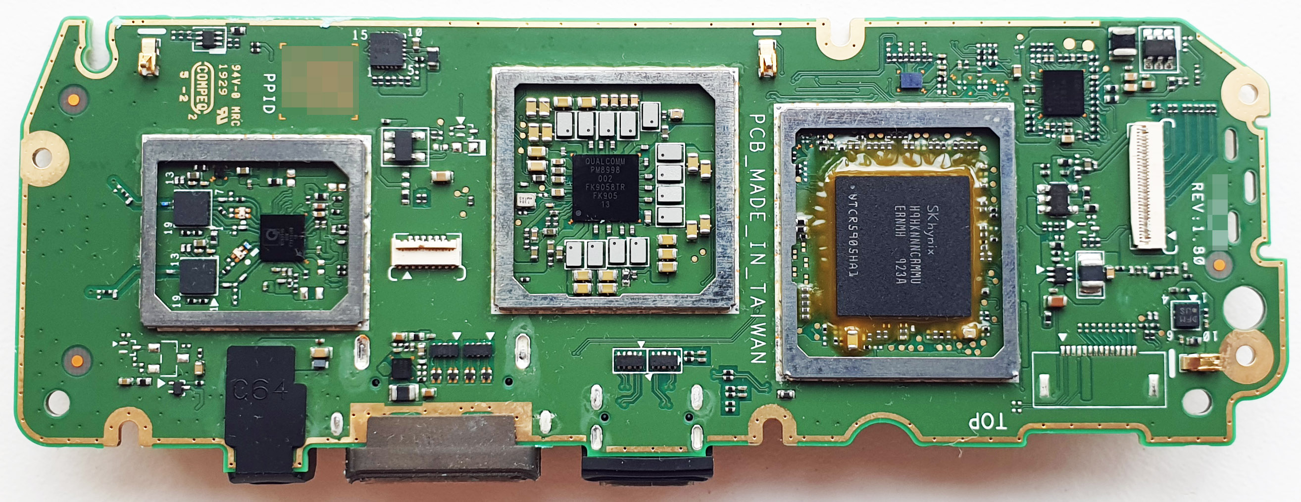
Because I really like to be able to read the part numbers on all the parts, here’s a couple more detail images of portions that didn’t photograph clearly in the above images.
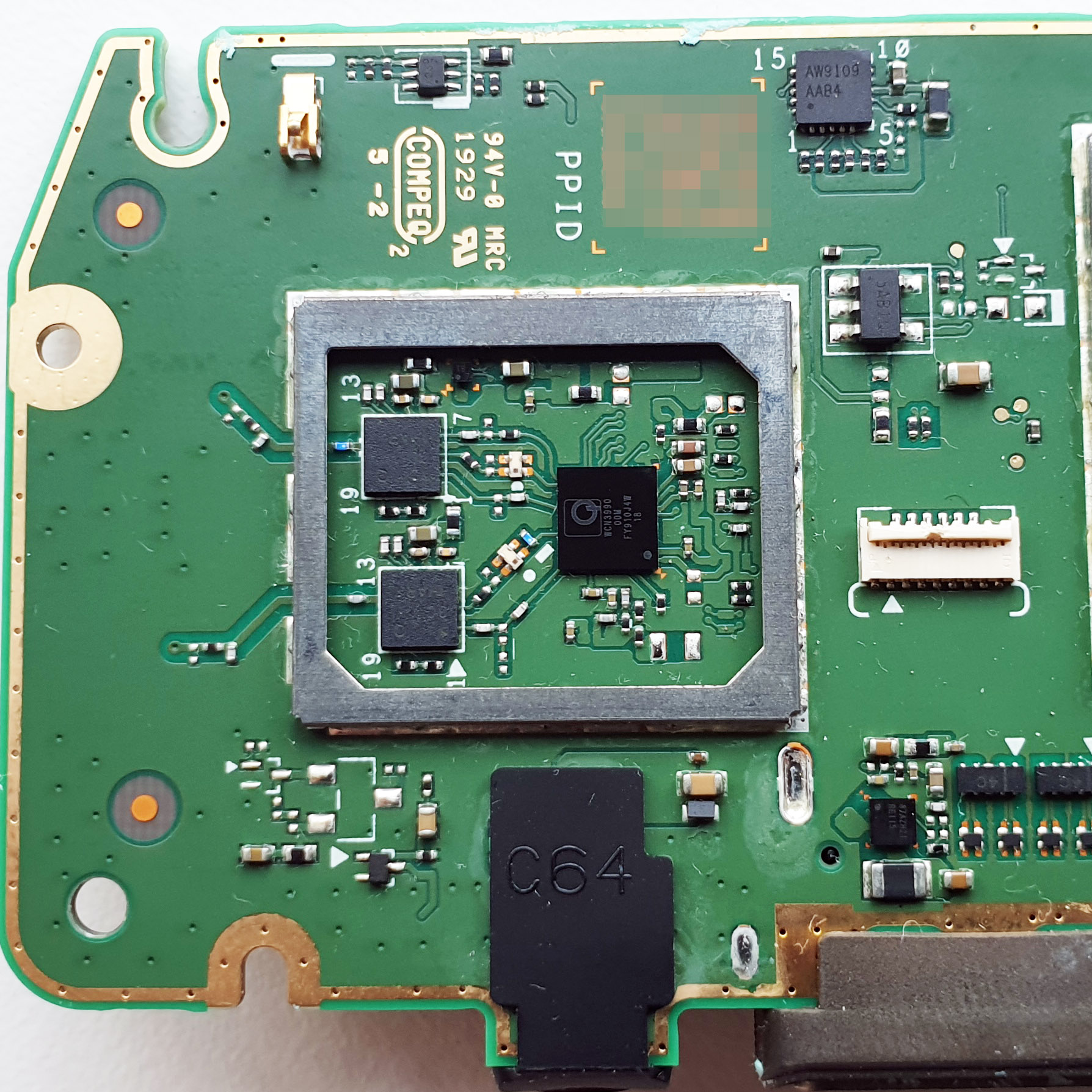
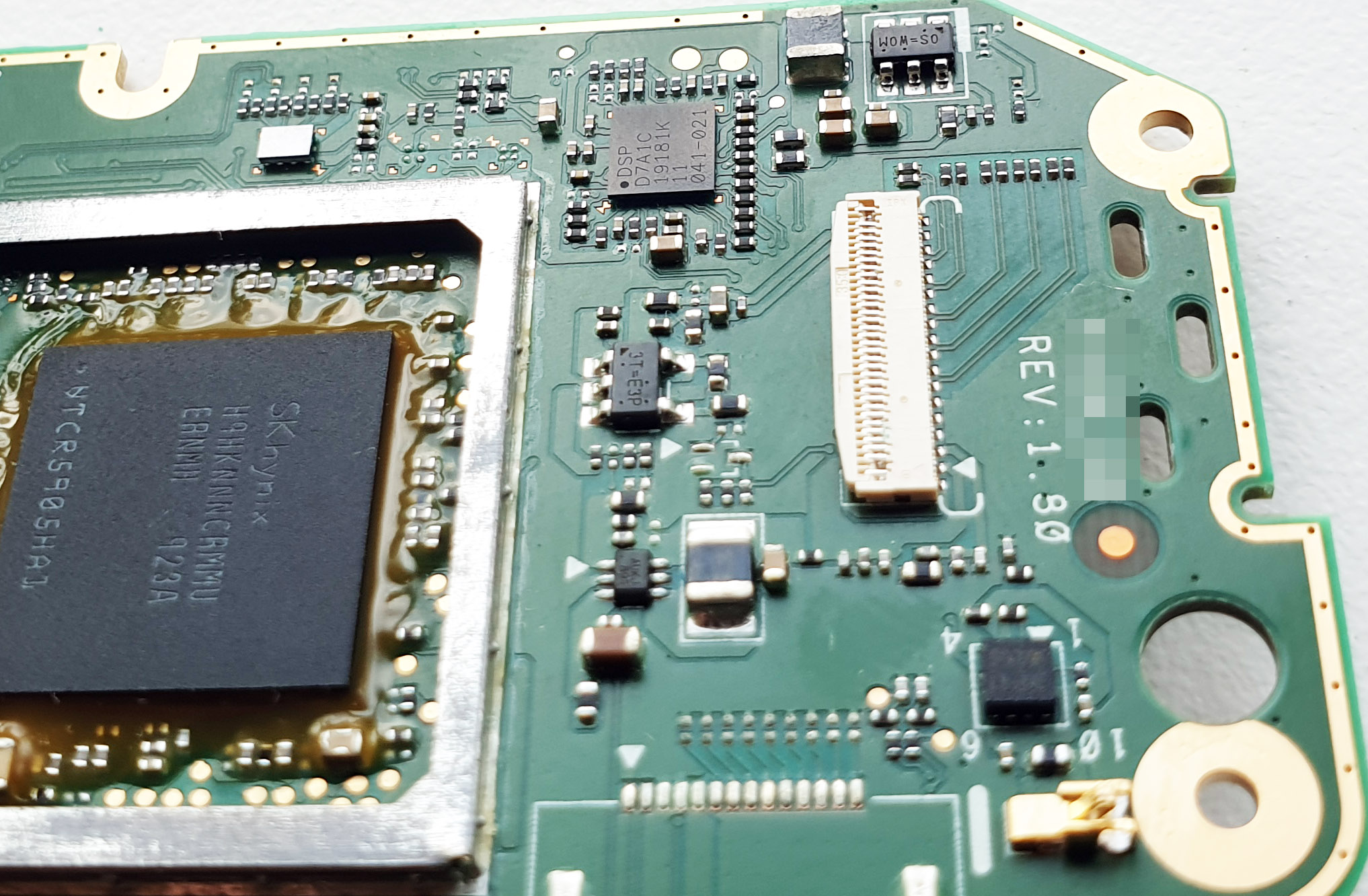
This ware was donated to me by someone in person, but unfortunately the post-it note I had put on it to remind me who it was had long fallen off. My apologies; if you happen to see this, feel free to pop a note in the comments so you can be attributed for the contribution.
I made a point of not looking up the details of the ware before I did the teardown, so I could have a little fun figuring it out. While pulling it apart, the entire time I kept muttering to myself how this ware reeks of silicon valley startup with more money than sense. The hardware engineers who worked on this were clearly professional, well-trained, and clever; but also, whoever the product manager was had some Opinions about design, and incorporated lots of cost-intensive high-tech “flexes”, most of which I’m pretty sure went unappreciated and/or unnoticed by anyone other than someone like me taking the thing apart. For example, the board shown above is encased in a thixomolded two-part magnesium thermal frame with heat pipes, precision-machined thermal conduction blocks and gobs and gobs of thermal paste, which then necessitated a fairly tricky assembly procedure, and some brand-name custom-designed antennae to work around the Faraday cage caused by the metal casing. You’ll also note that despite the whole assembly being stuck in a metal case, each circuit subsystem still had an RF cage over it – so it’s metal cages inside a metal cage. This project must have had one heck of a tooling budget.
This was all for the sake of a “clean” design that lacked any visible screws. I’d say it also lacked visible cooling vents but ironically the final design had prominent ribbed structures, but they weren’t used for cooling – they were purely cosmetic and sealed over with an inner bezel. I feel like most of the cost for the thermal frame could have been avoided if they just let some air flow through the product, but someone, somewhere, in the decision chain had a very strong opinion about the need for a minimalist design that left little room for compromise. I would lay good money that the argument “but Apple does it this way” was used more than once to drive a design decision and/or shame an engineer into retracting a compromise proposal. Anyways, I found this product to be an entertaining case study in over-engineering.
The Ware for April 2025 is two digits out of a TI-55 calculator display. The full display assembly and calculator IC can be seen below.
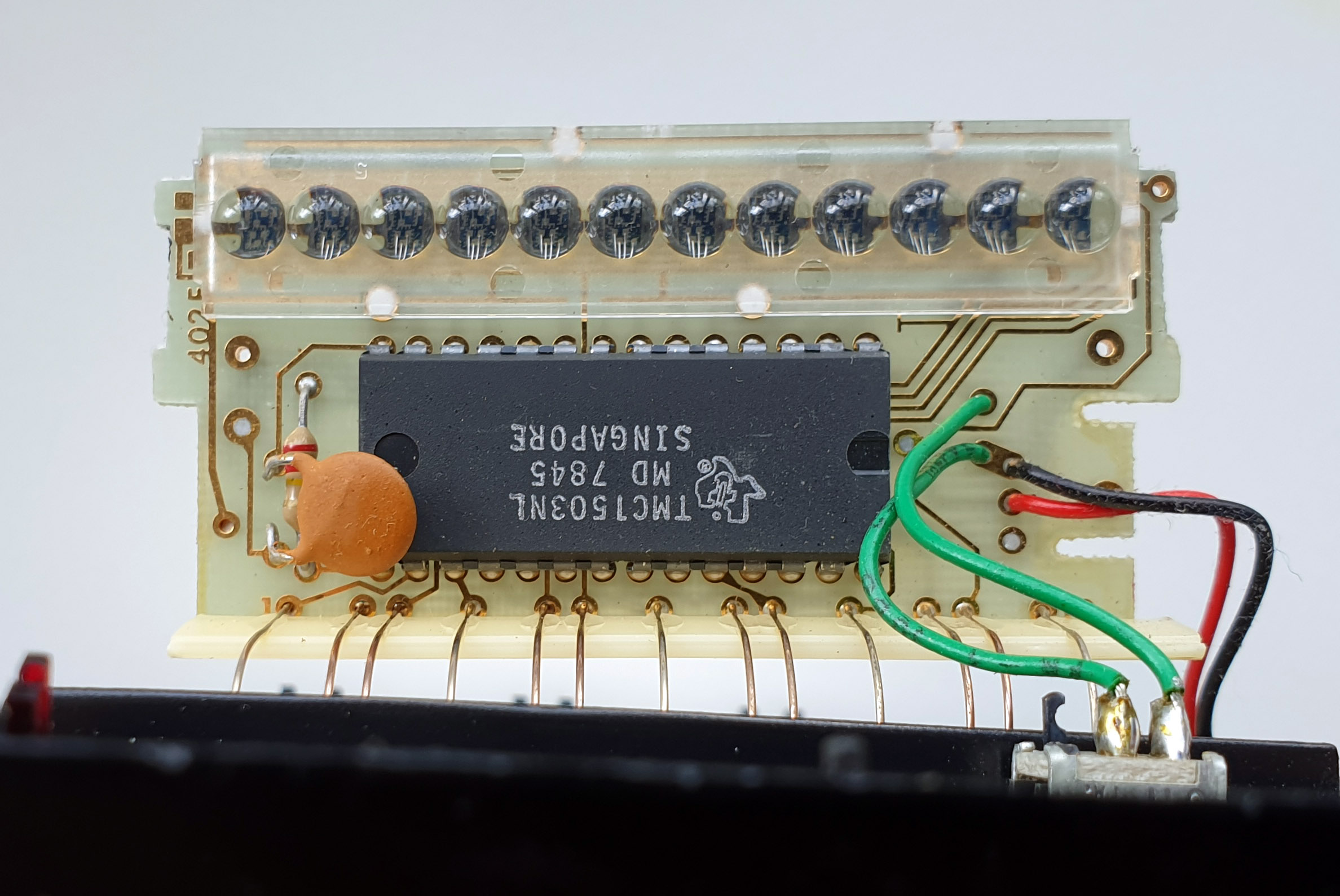
This was my father’s old calculator that he got back in 1979, which I recently recovered and lightly modified so that I could power it from a USB plug. I was getting frustrated with how buggy the “standard” calculator apps were, and this thing is perfect for doing taxes – I can crunch numbers without any fear of data being sucked into the cloud, or ads popping up. Even after 46 years, the TI-55 performs flawlessly – I can only aspire to build products with such evergreen utility and service life.
I took it apart, as I do to almost everything within arms reach of me, and was amused by the bonding error on the LED display. I’ve seen wirebonds repaired by hand before, my guess is someone in Taiwan back in 1978 spent a hot second pulling off a failed bond and redoing it on a manual bonding machine.
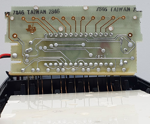
I thought it was interesting to include some more photos of the components because even back in 1970’s, the global nature of the supply chain was clear. Here is a calculator from “Texas Instruments”, but the chip was packaged in Singapore (probably not more than a half hour from where I live now!) and the display was bonded/assembled in Taiwan.
People speak of the outsourcing and globalization of electronics as some sort of recent phenomenon, as if electronics manufacturing plants were all originally in the USA, and only in the past couple decades migrated to Asia. However, if this calculator is any indicator of how supply chains worked almost 50 years ago, the outsource assembly of electronics to southeast Asia would seem to be a time-honored tradition dating from the dawn of consumer electronics.
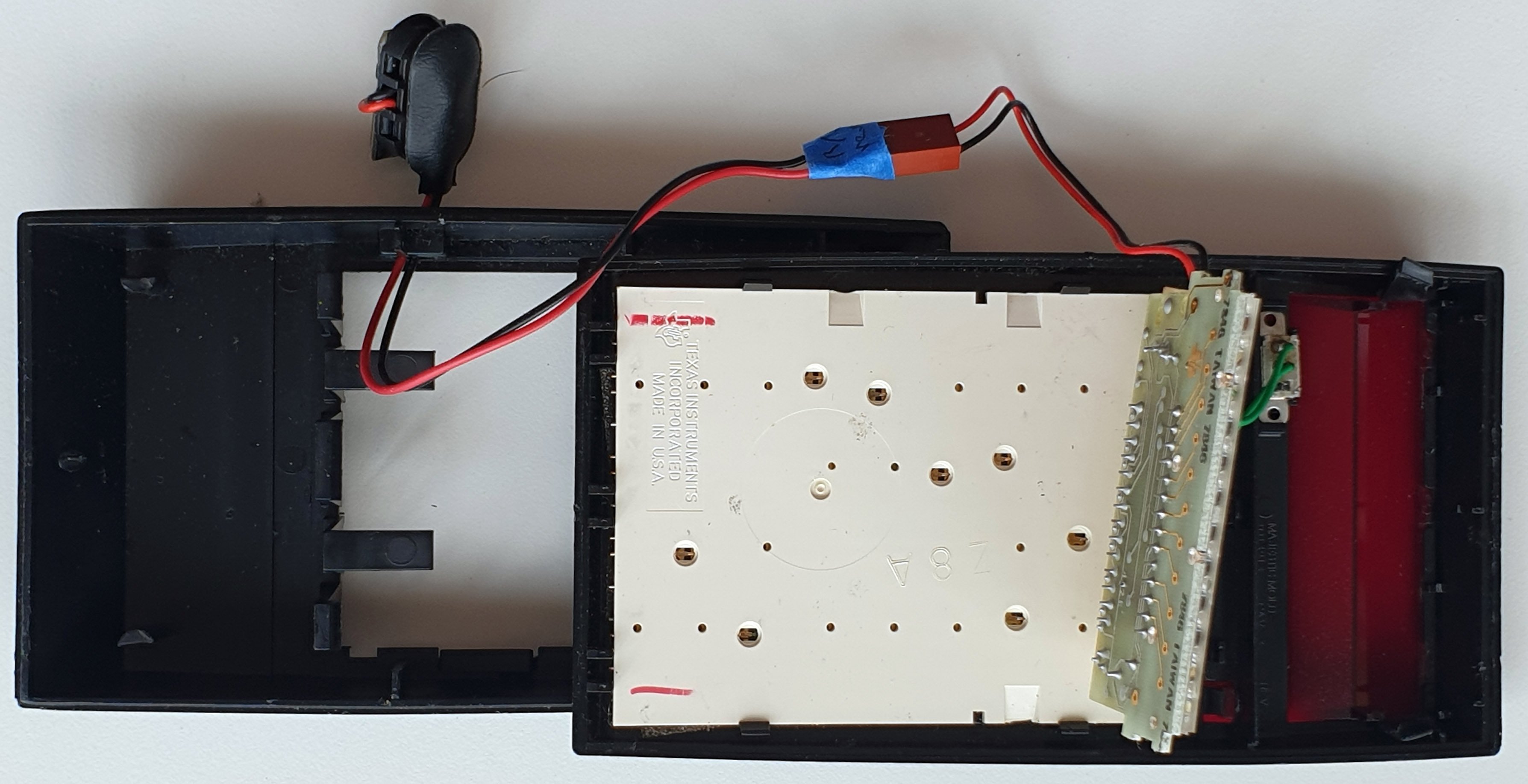
The keypad backing and plastic case bear “made in the USA” marks. So, while the semiconductors were packaged up in Asia, the injection molding and final assembly was done on a line somewhere in the US; the injection molder is identified as “Majestic Mold”. Injection molding is a whole separate and also very interesting supply chain story, but the short version is that I have seen some high-end specialty lines in the US (mostly medical and aerospace stuff) but the ecosystem of skilled labor, tools, raw material suppliers, machine repair specialists, recycling facilities and trade-secret know-how necessary to support cost-competitive injection molding has largely relocated to southeast Asia since the turn of the century.
I’ll give the prize this month to Adrian (unfortunately by the time I got around to clicking Joe’s image links, they were all 404’s). While nobody was able to guess the exact make/model of the LED, I did appreciate the image Adrian posted of a functioning display on his mastodon account. I was wondering what the “fingers” were on the metallization, and his image made it click for me. My guess is that the carrier lifetime was short enough on these older devices that regularly spaced fingers were needed to ensure uniform current density in the active region of the LED. Charge carriers can travel farther in today’s more pure wafers, and so modern LEDs don’t suffer as much of a brightness penalty from metallization blocking the active area.
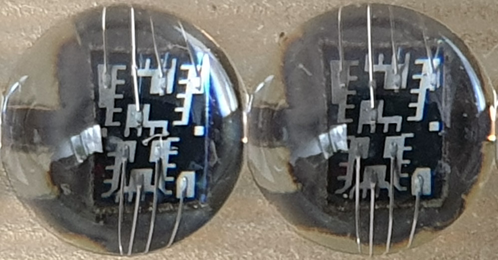
The Ware for this month is shown below:
It’s a tiny portion of a much larger ware, but for various reasons I think this is sufficient for someone to guess at least the type of ware this came from, if not the exact make/model.
There’s a particularly interesting bit about this ware, which you can see in the center of the left module – a tiny bit of wire that is out of place! It’s pretty rare to find small manufacturing defects like this in the wild. So far, this defect hasn’t caused a functional issue but I suppose some day it may. I wonder if this is a so-called “tin whisker” (i.e., a piece of metal that will keep growing with time until it causes a fault), or if it is just an errant bit of metal left over as an artifact of the manufacturing process. Only time will tell, I suppose!