Cryptography tells us how to make a chain of trust rooted in special-purpose chips known as secure elements. But how do we come to trust our secure elements? I have been searching for solutions to this thorny supply chain problem. Ideally, one can directly inspect the construction of a chip, but any viable inspection method must verify the construction of silicon chips after they have been integrated into finished products, without having to unmount or destroy the chips (“in situ“). The method should also ideally be cheap and simple enough for end users to access.
This post introduces a technique I call “Infra-Red, In Situ” (IRIS) inspection. It is founded on two insights: first, that silicon is transparent to infra-red light; second, that a digital camera can be modified to “see” in infra-red, thus effectively “seeing through” silicon chips. We can use these insights to inspect an increasingly popular family of chip packages known as Wafer Level Chip Scale Packages (WLCSPs) by shining infrared light through the back side of the package and detecting reflections from the lowest layers of metal using a digital camera. This technique works even after the chip has been assembled into a finished product. However, the resolution of the imaging method is limited to micron-scale features.
This post will start by briefly reviewing why silicon inspection is important, as well as some current methods for inspecting silicon. Then, I will go into the IRIS inspection method, giving background on the theory of operation while disclosing methods and initial results. Finally, I’ll contextualize the technique and discuss methods for closing the gap between micron-scale feature inspection and the nanometer-scale features found in today’s chip fabrication technology.
DOI: 10.48550/arXiv.2303.07406
Side Note on Trust Models
Many assume the point of trustable hardware is so that a third party can control what you do with your computer – like the secure enclave in an iPhone or a TPM in a PC. In this model, users delegate trust to vendors, and vendors do not trust users with key material: anti-tamper measures take priority over inspectability.
Readers who make this assumption would be confused by a trust method that involves open source and user inspections. To be clear, the threat model in this post assumes no third parties can be trusted, especially not the vendors. The IRIS method is for users who want to be empowered to manage their own key material. I acknowledge this is an increasingly minority position.
Why Inspect Chips?
The problem boils down to chips being literal black boxes with nothing but the label on the outside to identify them.
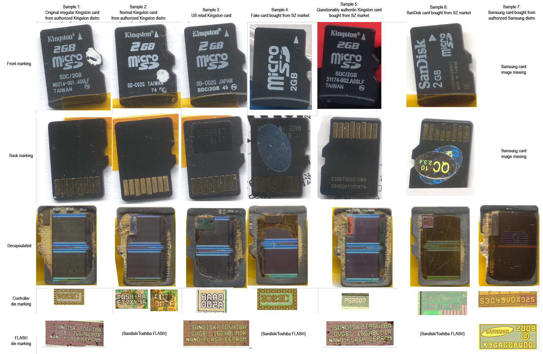
For example, above is a study I performed surveying the construction of microSD cards in an effort to trace down the root cause of a failed lot of products. Although every microSD card ostensibly advertised the same product and brand (Kingston 2GB), a decap study (where the exterior black epoxy is dissolved using a strong acid revealing the internal chips while destroying the card) revealed a great diversity in internal construction and suspected ghost runs. The take-away is that labels can’t be trusted; if you have a high-trust situation, something more is needed to establish a device’s internal construction than the exterior markings on a chip’s package.
What Are Some Existing Options for Inspecting Chips?
There are many options for inspecting the construction of chips; however, all of them suffer from a “Time Of Check versus Time Of Use” (TOCTOU) problem. In other words, none of these techniques are in situ. They must be performed either on samples of chips that are merely representative of the exact device in your possession, or they must be done at remote facilities such that the sample passes through many stranger’s hands before returning to your possession.

Scanning Electron Microscopy (SEM), exemplified above, is a popular method for inspecting chips (image credit: tmbinc). The technique can produce highly detailed images of even the latest nanometer-scale transistors. However, the technique is destructive: it can only probe the surface of a material. In order to image transistors one has to remove (through etching or polishing) the overlying layers of metal. Thus, the technique is not suitable for in situ inspection.
X-rays, exemplified in the above image of a MTK6260DA , are capable of non-destructive in situ inspection; anyone who has traveled by air is familiar with the applicability of X-rays to detect foreign objects inside locked suitcases. However, silicon is nearly transparent to the types of X-rays used in security checkpoints, making it less suitable for establishing the contents of a chip package. It can identify the size of a die and the position of bond wires, but it can’t establish much about the pattern of transistors on a die.
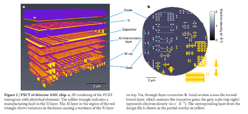
X-Ray Ptychography is a technique using high energy X-rays that can non-destructively establish the pattern of transistors on a chip. The image above is an example of a high-resolution 3D image generated by the technique, as disclosed in this Nature paper.

It is a very powerful technique, but unfortunately it requires a light source the size of a building, such as the Swiss Light Source (SLS) (donut-shaped building in the image above), of which there are few in the world. While it is a powerful method, it is impractical for inspecting every end user device. It also suffers from the TOCTOU problem in that your sample has to be mailed to the SLS and then mailed back to you. So, unless you hand-carried the sample to and from the SLS, your device is now additionally subject to “evil courier” attacks.
Optical microscopy – with a simple benchtop microscope, similar to those found in grade-school classrooms around the world – is also a noteworthy tool for inspecting chips that is easier to access than the SLS. Visible light can be a useful tool for checking the construction of a chip, if the chip itself has not been obscured with an opaque, over-molded plastic shell.
Fortunately, in the world of chip packaging, it has become increasingly popular to package chips with no overmolded plastic. The downside of exposing delicate silicon chips to possible mechanical abuse is offset by improved thermal performance, better electrical characteristics, smaller footprints, as well as typically lower costs when compared to overmolding. Because of its compelling advantages this style of packaging is ubiquitous in mobile devices. A common form of this package is known as the “Wafer Level Chip Scale Package” (WLCSP), and it can be optically inspected prior to assembly.
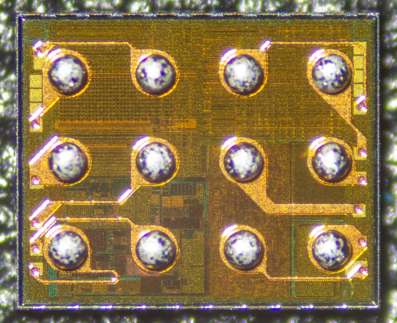
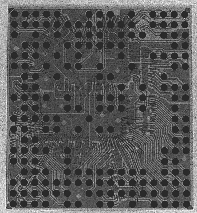
Above is an example of such a package viewed with an optical microscope, prior to attachment to a circuit board. In this image, the back side of the wafer is facing away from us, and the front side is dotted with 12 large silvery circles that are solder balls. The spacing of these solder balls is just 0.5mm – this chip would easily fit on your pinky nail.
The imaged chip is laying on its back, with the camera and light source reflecting light off of the top level routing features of the chip, as illustrated in the cross-section diagram above. Oftentimes these top level metal features take the form of a regular waffle-like grid. This grid of metal distributes power for the underlying logic, obscuring it from direct optical inspection.
Note that the terms “front” and “back” are taken from the perspective of the chip’s designer; thus, once the solder balls are attached to the circuit board, the “front side” with all the circuitry is obscured, and the plain silvery or sometimes paint-coated “back side” is what’s visible.
As a result, these chip packages look like opaque silvery squares, as demonstrated in the image above. Therefore front-side optical microscopy is not suitable for in situ inspection, as the chip must be removed from the board in order to see the interesting bits on the front side of the chip.
The IRIS Inspection Method
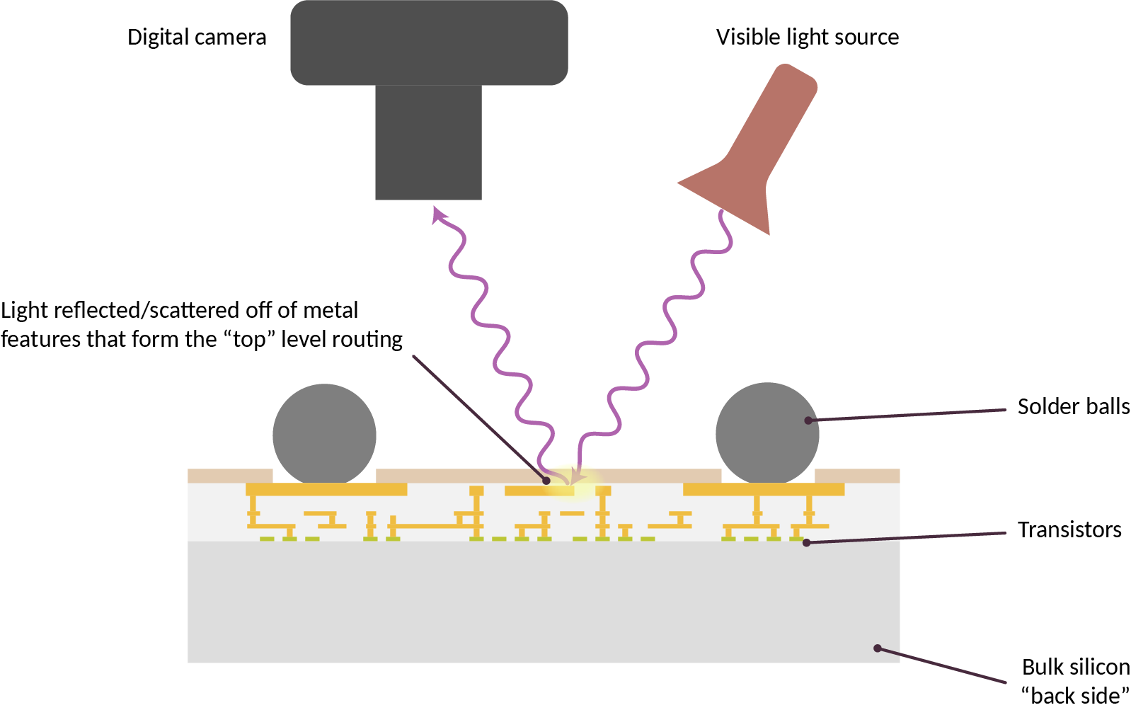
The Infra-Red, In Situ (IRIS) inspection method is capable of seeing through a chip already attached to a circuit board, and non-destructively imaging the construction of a chip’s logic.
Here’s a GIF that shows what it means in practice:
We start with an image of a WLCSP chip in visible light, assembled to a finished PCB (in this case, an iPhone motherboard). The scene is then flooded with 1070 nm infrared light, causing it to take on a purplish hue. I then turn off the visible light, leaving only the infrared light on. The internal structure of the chip comes into focus as we adjust the lens. Finally, the IR illuminator is moved around to show how the chip’s internal metal layers glint with light reflected through the body of the silicon.
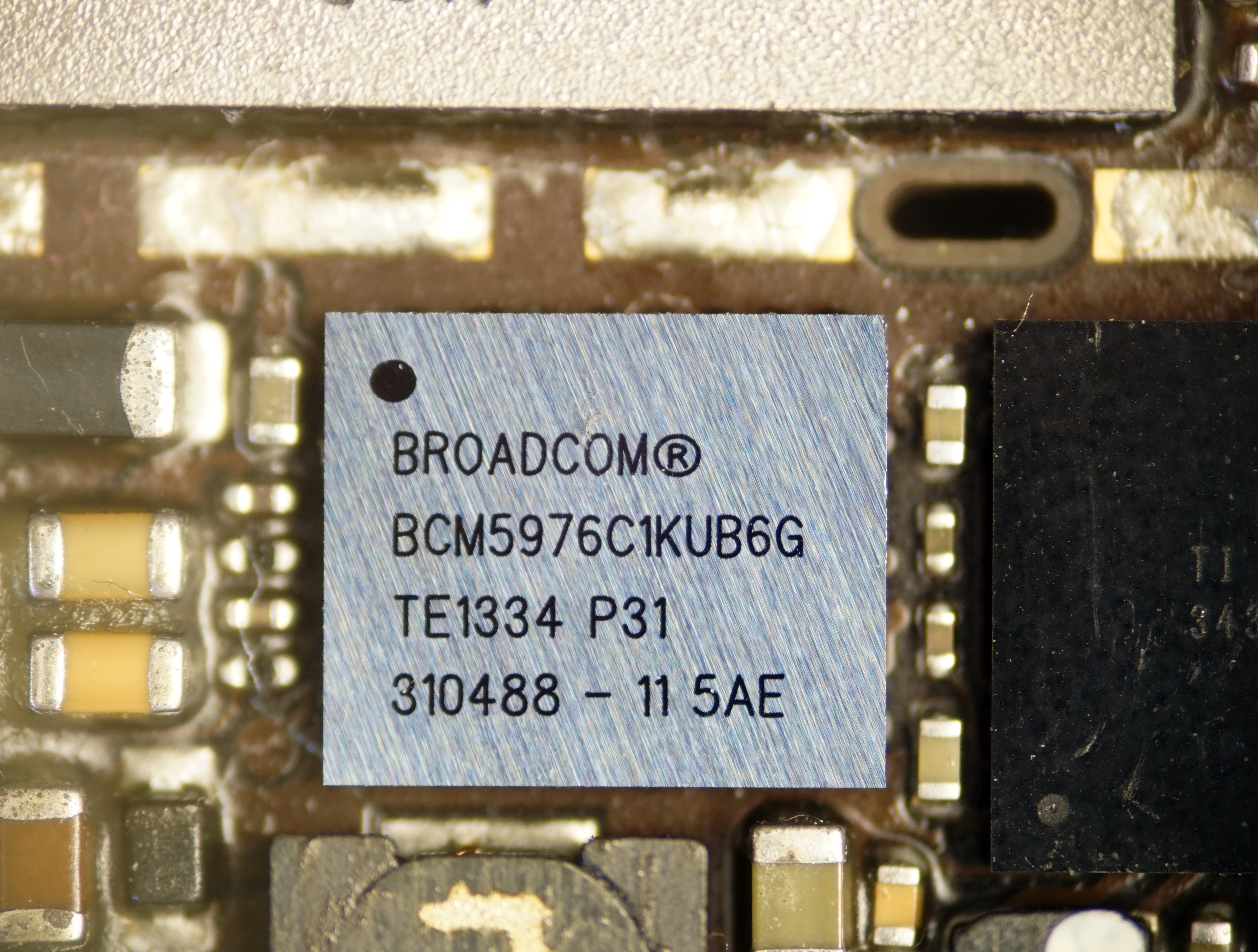
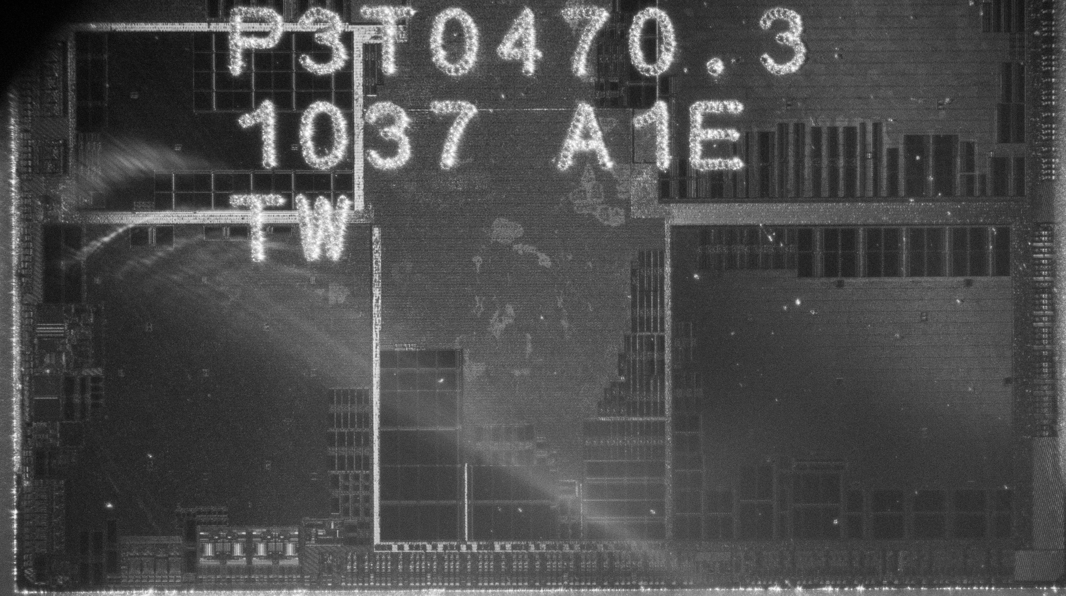
Here is a still image of the above chip imaged in infra-red, at a higher resolution:

The chip is the BCM5976, a capacitive touchscreen driver for older models of iPhones. The image reveals the macro-scopic structure of the chip, with multiple channels of data converters on the top right and right edge, along with several arrays of non-volatile memory and RAM along the lower half. From the top left extending to the center is a sea of standard cell logic, which has a “texture” based on the routing density of the metal layers. Remember, we’re looking through the backside of the chip, so the metal layer we’re seeing is mostly M1 (the metal connecting directly to the transistors). The diagonal artifacts apparent through the standard cell region are due to a slight surface texture left over from wafer processing.
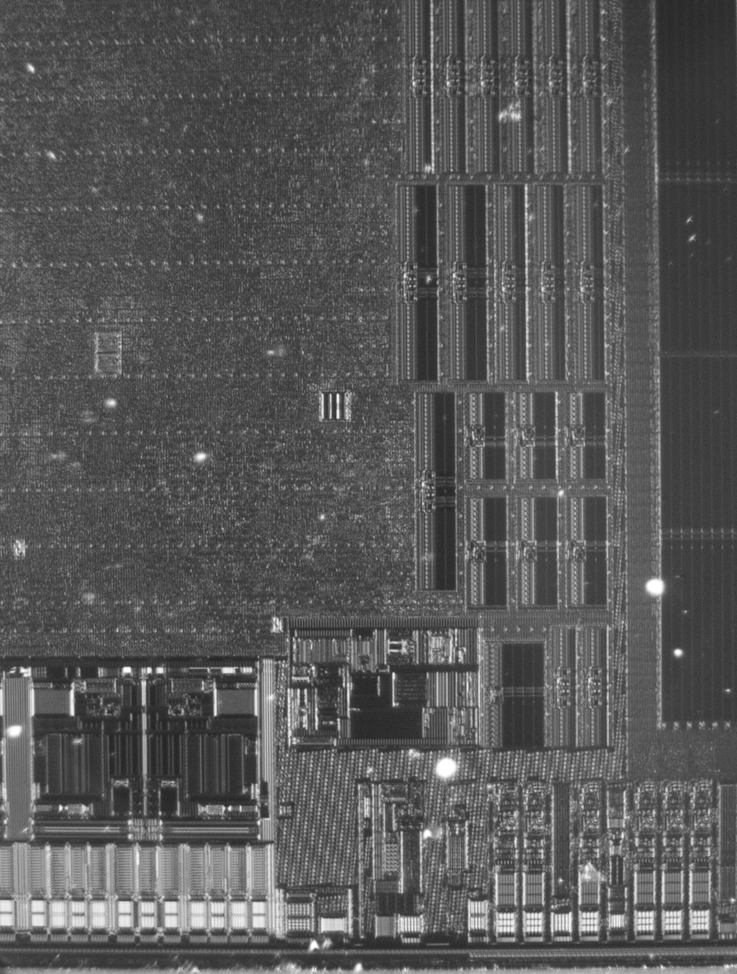
Below is the region in the pink rectangle at a higher magnification (click on the image to open a full-resolution version):
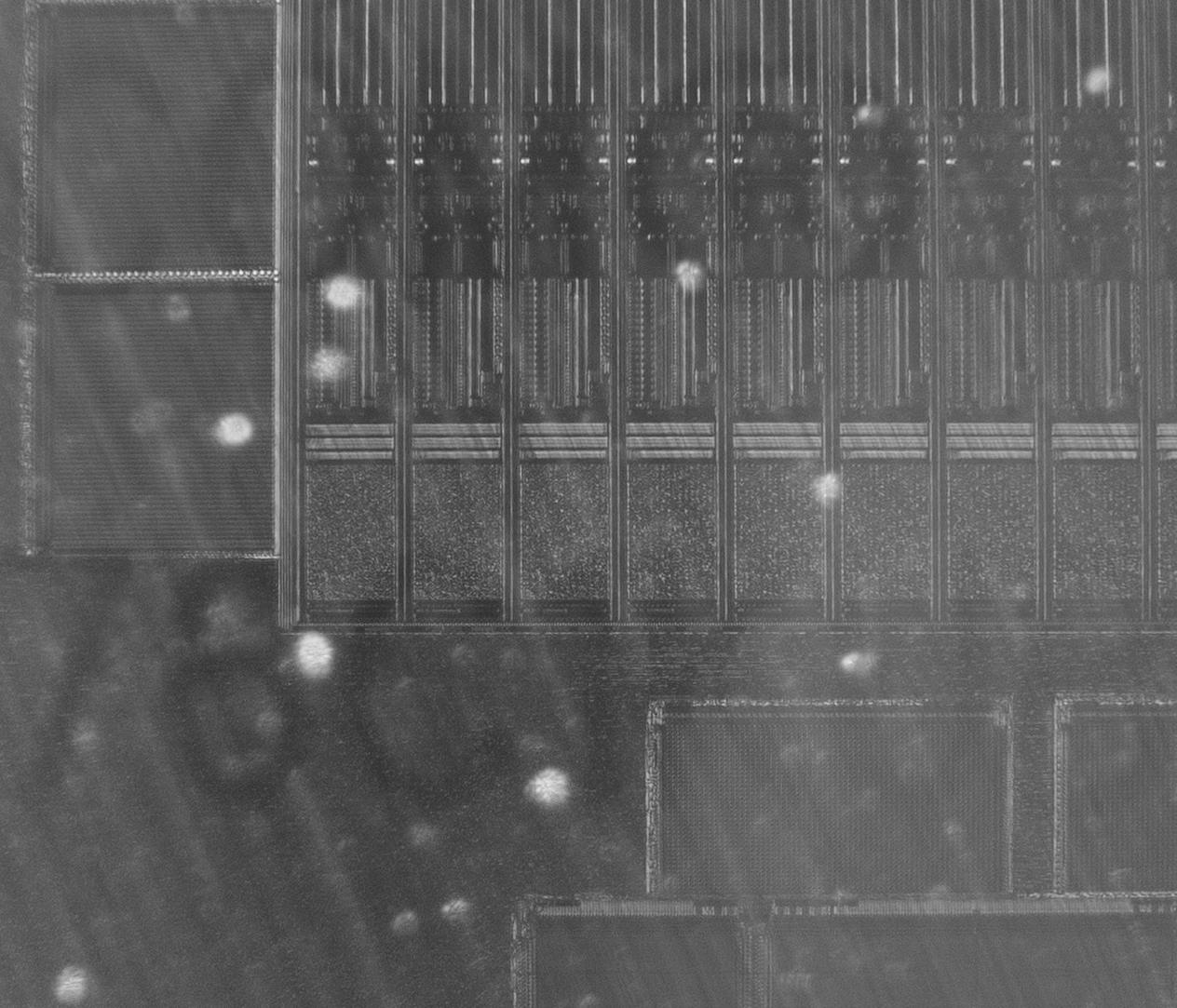
The magnified region demonstrates the imaging of meso-scopic structures, such as the row and structure column of memory macros and details of the data converters.
The larger image is 2330 pixels wide, while the chip is 3.9 mm wide: so each pixel corresponds to about 1.67 micron. To put that in perspective, if the chip were fabricated in 28 nm that would correspond to a “9-track” standard cell logic gate being 0.8 microns tall (based on data from Wikichip). Thus while these images cannot precisely resolve individual logic gates, the overall brightness of a region will bear a correlation to the type and density of logic gate used. Also please remember that IRIS is still at the “proof of concept” stage, and there are many things I’m working on to improve the image quality and fidelity.
Here’s another demo of the technique in action, on a different iPhone motherboard:
How Does It Work?
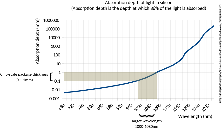
Silicon goes from opaque to transparent in the range of 1000 nm to 1100 nm (shaded band in the illustration below). Above 1100 nm, it’s as transparent as a pane of glass; below 1000 nm, it rapidly becomes more opaque than the darkest sunglasses.
Meanwhile, silicon-based image sensors retain some sensitivity in the near-to-short wave IR bands, as illustrated below.
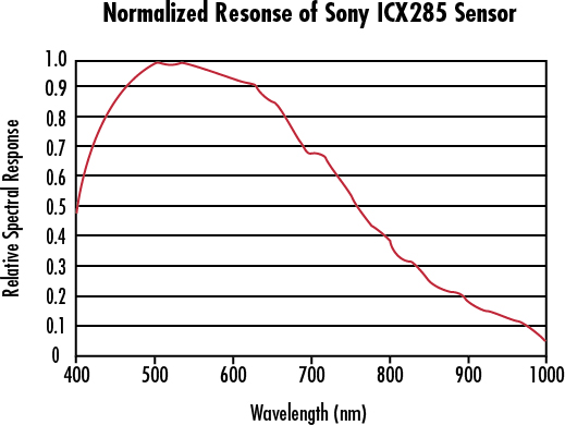
Between these two curves, there is a “sweet spot” where standard CMOS sensors retain some sensitivity to short-wave infrared, yet silicon is transparent enough that sufficient light passes through the layer of bulk silicon that forms the back side of a WLCSP package to do reflected-light imaging. More concretely, at 1000 nm a CMOS sensor might have 0.1x its peak sensitivity, and a 0.3 mm thick piece of silicon may pass about 10% of the incident light – so overall we are talking about a ~100x reduction in signal intensity compared to visible light operations. While this reduction is non-trivial, it is surmountable with a combination of a more intense light source and a longer exposure time (on the order of several seconds).
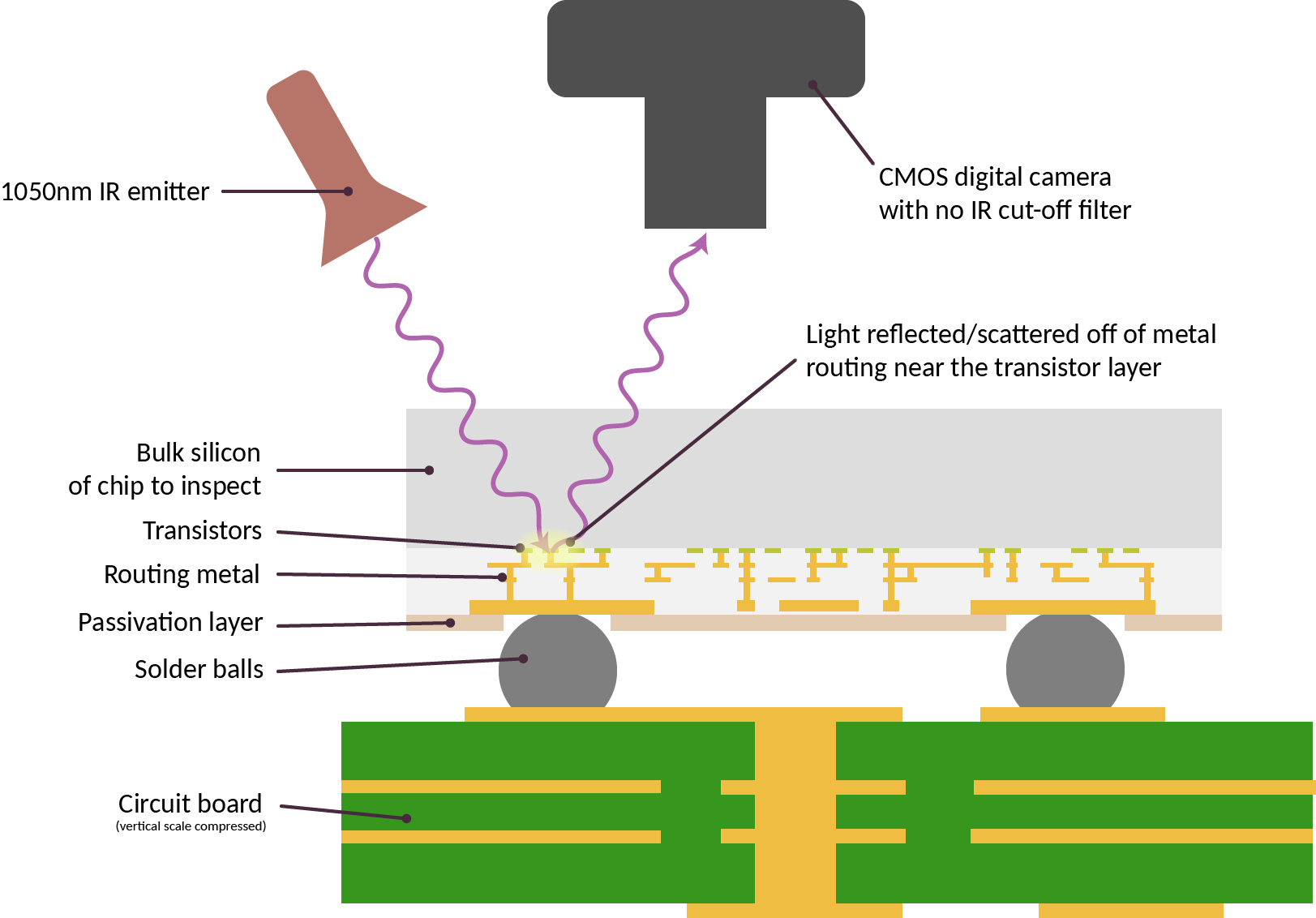
Above is a cross-section schematic of the IRIS inspection setup. Here, the sample for inspection is already attached to a circuit board and we are shining light through the back side of the silicon chip. The light reflects off of the layers of metal closest to the transistors, and is imaged using a camera. Conceptually, it is fairly straightforward once aware of the “sweet spot” in infrared.
Two things need to be prepared for the IRIS imaging technique. First, the “IR cut-off filter” has to be removed from a digital camera. Normally, the additional infrared sensitivity of CMOS sensors is considered to be problematic, as it introduces color fidelity artifacts. Because of this excess sensitivity, all consumer digital cameras ship with a special filter installed that blocks any incoming IR light. Removing this filter can range from trivial to very complicated, depending on the make of the camera.
Second, we need a source of IR light. Incandescent bulbs and natural sunlight contain plenty of IR light, but the current demonstration setup uses a pair of 1070 nm, 100 mA IF LED emitters from Martech, connected to a simple variable current power supply (in practice any LED around 1050nm +/- 30nm seems to work fairly well).
To give credit where it’s due, the spark for IRIS came from a series of papers referred to me by Dmitry Nedospadov during a chance meeting at CCC. One published example is “Key Extraction Using Thermal Laser Stimulation” by Lohrke et al, published in IACR Transactions on Cryptographic Hardware and Embedded Systems (DOI:10.13154/tches.v2018.i3.573-595). In this paper, a Phemos-1000 system by Hamamatsu (a roughly million dollar tool) uses a scanning laser to do optical backside imaging of an FPGA in a flip-chip package. More recently, I discovered a photo feed by Fritzchens Fritz demonstrating a similar technique, but using a much cheaper off-the-shelf Sony NEX-5T. Since then, I have been copying these ideas and improving upon them for practical application in supply chain/chip verification.
How Can I Try It Out?
While “off the shelf” solutions like the Phemos-1000 from Hamamatsu can produce high-resolution backside images of chips, the six or seven-figure price tag puts it out of reach of most practical applications. I have been researching ways to scale this cost down to something more accessible to end-users.
In the video below, I demonstrate how to modify an entry-level digital inspection camera, purchasable for about $180, to perform IRIS inspections. The modification is fairly straightforward and takes just a few minutes. The result is an inspection system that is capable of performing, at the very least, block-level verification of a chip’s construction.
For those interested in trying this out, this is the $180 camera and lens combo from Hayear (link contains affiliate code) used in the video. If you don’t already have a stand for mounting and focusing the camera, this one is pricey, but solid. You’ll also need some IR LEDs like this one to illuminate the sample. I have found that most LEDs with a 1050-1070 nm center wavelength works fairly well. Shorter wavelength LEDs are cheaper, but the incidentally reflected light off the chip’s outer surface tends to swamp the light reflected by internal metal layers; longer than 1100 nm, and the camera efficiency drops off too much and the image is too faint and noisy.
Of course, you can get higher quality images if you spend more money on better optics and a better camera. Most of the images shown in this post were taken with a Sony A6000 camera that was pre-modified by Kolari Vision. If you have a spare camera body laying around it is possible to DIY the IR cut-off filter removal; YouTube has several videos showing how.
The modified camera was matched with either the optics of the previously-linked Hayear inspection scope, or directly attached to a compound microscope via a C-mount to E-mount adapter.
Another Sample Image
I’ve been using an old Armada610 chip I had laying around for testing the setup. It’s ideal for testing because I know the node it was fabbed in (55 nm) and the package is a bare flip-chip BGA. FCBGA is a reasonably common package type, but more importantly for IRIS, the silicon is pre-thinned and mirror-polished. This is done to improve thermal performance, but it also makes for very clean backside images.
Above is what the chip looks like in visible light.

And here’s the same chip, except in IR. The light source is shining from the top right, and already you can see some of the detail within the chip. Note: the die is 8mm wide.
Above is the lower part of the chip, taken at a higher magnification. Here we can start to clearly make out the shapes of memory macros, I/O drivers, and regions of differing routing density in the standard cell logic. The die is about 4290 pixels across in this image, or about 1.86 microns per pixel.
And finally, above is the boxed region in the previous image, but a higher magnification (you can click on any of the images for a full-resolution version). Here we can make out the individual transistors used in I/O pads, sense amps on the RAM macros, and the texture of the standard cell logic. The resolution of this photo is roughly 1.13 microns per pixel – around the limit of what could be resolved with the 1070 nm light source – and a hypothetical “9-track” standard cell logic gate might be a little over a pixel tall by a couple pixels wide, on average.
Discussion
IRIS inspection reveals the internal structure of a silicon chip. IRIS can do this in situ (after the chip has been assembled into a product), and in a non-destructive manner. However, the technique can only inspect chips that have been packaged with the back side of the silicon exposed. Fortunately, a fairly broad and popular range of packages such as WLCSP and FCBGA already expose the back side of chips.
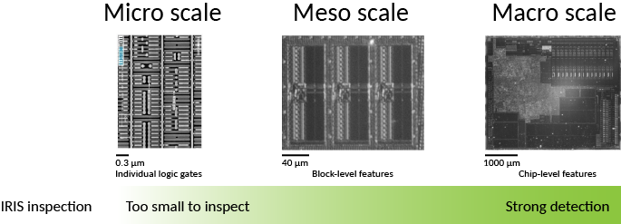
Above: Various size scales found on a chip, in relationship to IRIS capabilities.
IRIS cannot inspect the smallest features of a chip. The diagram above illustrates the various size scales found on a chip and relates it to the capabilities of IRIS. The three general feature ranges are prefixed with micro-, meso-, and macro-. On the left hand side, “micro-scale” features such as individual logic gates will be smaller than a micron tall. These are not resolvable with infra-red wavelengths and as such not directly inspectable via IRIS, so the representative image was created using SEM. The imaged region contains about 8 individual logic gates.
In the middle, we can see that “meso-scale” features can be constrained in size and identity. The representative image, taken with IRIS, shows three RAM “hard macros” in a 55 nm process. Individual row sense amplifiers are resolvable in this image. Even in a more modern sub-10 nm process, we can constrain a RAM’s size to plus/minus a few rows or columns.
On the right, “macro-scale” features are clearly enumerable. The number and count of major functional blocks such as I/O pads, data converters, oscillators, RAM, FLASH, and ROM blocks are readily identified.
IRIS is a major improvement over simply reading the numbers printed on the outside of a chip’s package and taking them at face value. It’s comparable to being able to X-ray every suitcase for dangerous objects, versus accepting suitcases based solely on their exterior size and shape.
Even with this improvement, malicious changes to chips – referred to as “hardware trojans” – can in theory remain devilishly difficult to detect, as demonstrated in “Stealthy Dopant-Level Hardware Trojans” by Becker, et al (2013). This paper proposes hardware trojans that only modulate the doping of transistors. Doping modifications would be invisible to most forms of inspection, including SEM, X-Ray ptychography, and IRIS.
The good news is that the attacks discussed (Becker, 2013) are against targets that are entirely unhardened against hardware trojans. With a reasonable amount of design-level hardening, we may be able to up the logic footprint for a hardware trojan into something large enough to be detected with IRIS. Fortunately, there is an existing body of research on hardening chips against trojans, using a variety of techniques including logic locking, built in self test (BIST) scans, path delay fingerprinting, and self-authentication methods; for an overview, see “Integrated Circuit Authentication” by Tehranipoor.
IRIS is a necessary complement to logic-level hardening methods, because logic-only methods are vulnerable to bypasses and emulation. In this scenario, a hardware trojan includes extra circuitry to evade detection by spoofing self-tests with correct answers, like a wolf carrying around a sheep’s costume that it dons only when a shepherd is nearby. Since IRIS can constrain meso-scale to macro-scale structure, we can rule out medium-to-large scale circuit modifications, giving us more confidence in the results of the micro-scale verification as reported by logic-level hardening methods.
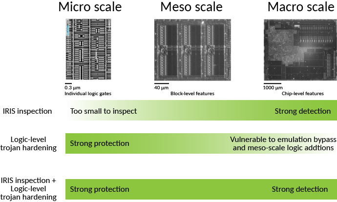
Above: Comparison of the detection-vs-protection trade offs of logic level hardening and IRIS inspection.
Thus, IRIS can be used in conjunction with logic-level trojan hardening to provide an overall high-confidence solution in a chip’s construction using non-destructive and in situ techniques, as illustrated above.
The primary requirement of the logic-level hardening method is that it must not be bypassable with a trivial amount of logic. For example, simple “logic locking” (a method of obfuscating logic which in its most basic form inserts X(N)ORs in logic paths, requiring a correct “key” to be applied to one input of the X(N)ORs to unlock proper operation) could be bypassed with just a few gates once the key is known, so this alone is not sufficient. However, a self-test mechanism that blends state from “normal runtime” mode and “self test” mode into a checksum of some sort could present a sufficiently high bar. In such a stateful verification mechanism, the amount of additional logic required to spoof a correct answer is proportional to the amount of state accumulated in the test. Thus, one can “scale up” the coverage of a logic-level test by including more state, until the point where any reliable bypass would be large enough to be detected by IRIS (thanks to jix for pointing me in the right direction!). The precise amount of state would depend on the process geometry: smaller process geometries would need more state.
Under the assumption that each extra bit would imply an additional flip flop plus a handful of gates, a back-of-the-envelope calculation indicates a 28 nm process would require just a few bits of state in the checksum. In this scenario, the additional trojan logic would modify several square microns of chip area, and materially change the scattering pattern of infra-red light off of the chip in the region of the modification. Additional techniques such as path delay fingerprinting may be necessary to force the trojan logic to be spatially clustered, so that the modification is confined to a single region, instead of diffused throughout the standard cell logic array.
Summary and Future Direction
IRIS is a promising technique for improving trust in hardware. With a bit of foresight and planning, designers can use IRIS in conjunction with logic hardening to gain comprehensive trust in a chip’s integrity from micro- to macro-scale. While the technique may not be suitable for every chip in a system, it fits comfortably within the parameters of chips requiring high assurance such as trust roots and secure enclaves.
Of course, IRIS is most effective when combined with open source chip design. In closed source chips, we don’t know what we’re looking at, or what we’re looking for; but with open source chips we can use the design source to augment the capabilities of IRIS to pinpoint features of interest.
That being said, I’m hoping that IR-capable microscopes become a staple on hardware hacker’s workbenches, so we can start to assemble databases of what chips should look like – be they open or closed source. Such a database can also find utility in everyday supply chain operations, helping to detect fake chips or silent die revisions prior to device assembly.
Over the coming year, I hope to improve the core IRIS technique. In addition to upgrading optics and adding image stitching to my toolbox, digitally controlling the angle and azimuth of incident light should play a significant role in enhancing the utility of IRIS. The sub-wavelength features on a chip interact with incident light like a hologram. By modifying the azimuth and angle of lighting, we can likely glean even more information about the structure of the underlying circuitry, even if they are smaller than the diffraction limit of the system.
A bit further down the road, I’d like to try combining IRIS with active laser probing techniques, where IRIS is used to precisely locate a spot that is then illuminated by an intense laser beam. While this has obvious applications in fault induction, it can also have applications in verification and chip readout. For example, the localized thermal stimulation of a laser can induce the Seeback effect, creating a data-dependent change in power consumption detectable with sensitive current monitors. I note here that if physical tamper-resistance is necessary, post-verification a chip can be sealed in opaque epoxy with bits of glitter sprinkled on top to shield it from direct optical manipulation attacks and evil-maid attacks. However, this is only necessary if these attacks are actually part of the threat model. Supply chain attacks happen, by definition, upstream of the end user’s location.
The other half of optical chip verification is an image processing problem. It’s one thing to have reference images of the chip, and it’s another thing to be able to take the image of a chip and compare it to the reference image and generate a confidence score in the construction of the chip. While I’m not an expert in image processing, I think it’s important to at least try and assemble a starter pipeline using well known image processing techniques. A turnkey feature extraction and comparison tool would go a long way toward making IRIS a practically useful tool.
Ultimately, the hope is to create a verification solution that grows in parallel with the open source chip design ecosystem, so that one day we can have chips we can trust. Not only will we know what chips are intended to do, we can rest assured knowing they were built as intended, too.
This research is partially funded by a NGI Zero Entrust grant from NLnet and the European Commission, as well as by the donations of Github Sponsors.
Have you tried Photon Emission Microscopy? Look with your camera at these chips and turn them on without any external illumination. You should be able to see photons coming out of the chips during switching. This can be used to see which part of the chip is active and (with a very good microscope) even see which transistor is switching.
Also Laser Scanning Techniques exist: Monitor the current consumption while scanning over the active device with an IR Laser. If the laser touches active circuitry, the current consumption will wiggle.
Further googling words should include EMMI, PEM, OBRICH, TIVA, IR-LIT :-)
I looked into the photon emission, you need a cooled camera with a very low dark current, and these are wicked expensive. Something to try, but the price tag makes it inaccessible for routine end user applications.
The post actually cites previous laser scanning techniques in the “discussion” section, exactly of the type you have mentioned. It is on the far-out roadmap of things to try someday.
How low of a dark current? I’m thinking of something like the imx533 which can be found nicely packaged with TEC cooling from QHY and ZWO (asi533mm [mono] or 533mc [color]) and has a readout noise as low as 1.0e.
Here’s a paper I’m using as a reference for trying to figure this out:
https://eprint.iacr.org/2017/822.pdf
The claim is the photons are 1330nm in wavelength. Another paper, I can’t seem to find it right now, mentioned you might get “a few” photons over several seconds. So 1.0e is in the ballpark of being able to generate a signal larger than noise, except for the fact that the imx533 QE is vanishingly small around 1330nm. Once you factor in the QE, you might have more noise than signal.
I suspect in order to do this you need to use one of the III-V cooled cameras, which ups the cost from a few hundred bucks to a couple $10k’s price tag — plus dealing with export controls etc. etc. because of its utility in military-grade night vision. It’s pricey enough that I can’t just go out and acquire one to experiment with. If you do get one of these, I’d be curious to hear the results.
Ah thanks for the resource, I didn’t realize the wavelength would be that far into IR so the QE would definitely be a problem I think. The only cheaper alternative, which isn’t that cheap, would maybe be an InGaAs sensor, like the imx990/991. However, I think prices should be coming down in the next few years so having it on a roadmap for future development (regardless of the method) is exciting! Great work!
To clarify though, if I use my 533 and point it at a powered chip in a suitable environment, are you saying there is a chance of seeing something? Because I will absolutely attempt if so. I’m thinking about this in a similar sense to collecting photons from space. Many long exposures, calibrated with dark and bias frames, stacked to increase SNR.
The going rates of the imx990/991 sensors are in the $9k-$15k range from what I’ve seen, versus the imx678 (which has a QE of ~0.3 at 1000nm) for around $300-$500.
The imx533 should work. Googling around reveals some informal posts indicating it has a QE of ~0.1 at 1000nm. And yes, you can compensate for the reduced QE with a long exposure and noise reduction tricks (on my Sony A6000 I set it to “ISO100” (which is the lowest noise setting) and an exposure of 10-15 seconds). You can also just use a brighter light source.
Perhaps take a look at DIY astronomy? There was a cookbook CCD camera a few years back that detailed how to build cooling etc.
Totally cool!
The big downside I see here is that you can’t image the poly layers, and the lower metal layers will obscure the upper ones – this is likely good for answering the question “does it look like the right chip” not so good for “has that gate been messed with and wired to the right place”.
Also imaging features that require EUV to render with IR means you’re limited in which chips you can get low level data from
You’re exactly right about the downside, which is why it has to be combined with some sort of logic-level scanning to confirm the actual wiring and doping of the transistors. There’s a decent body of existing research around that which I’m catching up on, but the general idea is to use IR-scale verification to make sure there isn’t some larger bypass circuit around the scanning logic, which means you can trust the result of the logic scan.
That makes sense – mind you messing with scan chains is just a mux and some wires, not really large scale features
Separate thoughts
– I wonder if someone could quietly fab IR leds on security chips and exfiltrate data through the base (LEDs require special chemistry, but maybe lower energy IR LEDs might be doable in some weird case)
– you’re looking from the bottom, can you image blown fuses normally hidden by metal layers? ……
Right, the idea is to combine the scan chain with some additional logic that accumulates state in some sort of CRC. To make it really effective, you’d have to have the CRC accumulate partially based on data in “normal run mode” and then the rest in “scan chain mode”. This forces the attacker to compensate for at least the amount of state accrued in the “normal run time” mode, which increases the footprint of the bypass logic. The idea is to tilt the tables in favor of the verifier because in this case the verifier gets to “warm up” the state vector with an indeterminate amount of “normal run” data before switching into scan mode. The amount of state you need to accumulate scales with the size of the CRC, so you have a knob you can turn to increase the size of the bypass, at the expense of a larger state accumulator overhead.
I once upon a time worked for a nanophotonics startup and we would have loved to be able to fabricate any sort of light source into silicon. A lot of very smart people have thought very hard about this and there hasn’t been a way to do it that I know of yet with any sort of reasonable efficiency. You’d definitely see a spike in the power consumption for any appreciable amount of light emission. Of course, you could always just do a flip-chip die attach of an emitter into the silicon….and if your chip is fabricated in SOI you can even make waveguides to couple the light to where you want it to be. But these are quite macroscopic and would show up easily with visual inspection.
I would *love to* find some fuses and try to image them. I doubt they’ll show up, but who knows — depending on the style of fuse, it involves some fairly intense local heating that could alter the index of refraction in an area much larger than the fuse and maybe create a signal.
I’ve already imaged flash memory arrays in 250nm and in maybe 40nm-ish technologies…you can’t see individual bits. But you can make out the row/column drivers, even in the 40nm case. I think that’s because the geometry of the drive transistors doesn’t scale as well with process node due to the voltages involved.
This might be totally off the wall, and isn’t as simple as attaching an instrument to an inspection scope, but wouldn’t it be possible to “JTAG” as a verb the logic on these larger chips? I.e., attaching the ring to every trace going into/out of the chip, and eventually having a database of “known good” results from such a jig?
Or, maybe, this is already done or a superior method is used to scan the logic. It does, of course, make sense to combine the IR-scale verification with a logic scan, and trust the result of the logic scan if the IR-scale verification shows no bypass circuit.
You’re exactly right. The proposition is to “JTAG” the whole chip, but you also have to use IR-scale verification to ensure there isn’t a bypass that detects the JTAG mode and presents you an alternate reality during the scan mode.
This morning I didn’t know one could do such a thing.
Thanks for doing what you do!
I came across a die photo of the previous generation of nVidia GPUs that looks like it was made using the same technique:
https://wccftech.com/nvidia-flagship-ampere-gaming-gpu-ga102-gets-beautiful-die-shot/
That’s almost certainly Fritzchen Fritz’s work! His Flickr feed has images of a busted A100 that he photographed.
Do you have a link to their Flickr?
Here it is: https://www.flickr.com/photos/130561288@N04/52465673068/in/photostream/
Is there a reason none of the images display?
I don’t see the problem right now, but it’s possible my server got rate limited. Are there still problems with images showing up?
The problem is that this camera (i have one) can’t do long exposure, it doesn’t even have an exposure control.
it can be solved, with many limitation, with an image stacking software (as used in astrophoto) to improve the S/N Ratio.
i’m very tempted to remove the IR filter, i’m happy to learn that it’s easy to do (rarely the case). But it’s my only camera at the moment so it will have to wait.
removing the IR filter, on top of butchering the colors, will also significantly degrade the overall image quality for “normal use” by introducing a massive chromatic aberation. the optical system is calibrated for green light (unless you have some super apo thingy, but even then, they’re not built for IR).
I’m super interested in seeing any experimentation using a laser as a microscope illumination (i’m not talking about confocal, just simple reflected/transmitted light microscopy, but with a laser instead of a regular lamp).
i have a bunch of (old) microscope at home, but a good controlable laser (aka : not a pen) is expensive.
So…
When there is a need, there is a will. (and vice versa)
– I (very) destructively removed the IR filter of an old bresser mikro okular (don’t buy it, it’s crap).
– i’ve put a a strong filter for IR photography below the condenser, in order to remove all visible light and be monochomatic(-ish)
– i pushed my 12V@60watt halogen light to 11V (60w it way too much for normal use, i usually use it at 6 or 7v), which generate a lot of heat (and therefore IR)
– as you can see here https://i.imgur.com/sPILcA2.jpg it totally works
– i was so surprised as to a well it went that i put the IR cutoff filter under the objective to make sure i did’t mess up and the image went totally black. So it works just fine.
– observation in “near-IR only” under the microscope works just fine as long as you remove the IR cutoff.
– i tried to observe an old opamp (unpowered), i got either nothing, or some kind of diffraction pattern / stray light that shouldn’t be here, but no clear image of a die (not even a blurry one).
– Perhaps transmitted IR light observation juste won’t work. but i’ll try again for sure. until i make it works, or figure out why it doesn’t works
Okay, after drinking enough caffeine and random experimentation, i realized why transmitted light doesn’t work and why it probably won’t (non destructively)
[…] https://www.bunniestudios.com/blog/?p=6712https://www.youtube.com/watch?v=kfsVb0pEayU […]
Congratulations on another piece of fine art in technology hacking :)
Very interesting article!
An approach I have seen in archeological imaging was to take digital images from a single perspective with a hemisphere array of LEDs so that the viewer could then virtually shift the light source, making it easier to identify markings on the surface of the imaged object. Having a couple different IR sources.and then switching back and forth between them might make distinguishing small components in the images easier?
Nice results, Bunnie!
Riffing on what Scott asked about using JTAG to explore or verify other people’s chips…
I worked for a fabless DSP startup in the early Aughts, and at some point I was tasked with wrangling test vectors. We dedicated 4 or 5 BGA balls to our JTAG controller for anyone to probe, but I’ve never worked with mass-market microcontrollers that bonded out the scan chain to the package pins. And for security-conscious chips, I have to believe there is a way to disable JTAG entirely. Can they like blow a fuse once the unpackaged die passes manufacturing tests? (My company played no such clever games.)
I also remember that scan chains can be hierarchical and re-configured on-the-fly so you don’t have to wait a gazillion clock cycles to access a certain piece of state. This would imply that if you don’t know what’s inside the chip, you will have a challenging time accessing the whole scan chain. The chip ID ROM might be relatively easy to read via JTAG, but also easily forged.
When I was in the micro-electronics industry in imec I came in contact with the wafer defect inspection tools. These tools are optical and allow to detect defects much smaller than the wavelength used for inspection. This is done by scanning the wafer and looking at the modulation of the (zero order) reflected light. It only detect where there is a defect, the actual imaging of the defect than needs to happen on higher resolution tools like a electron microscope or so.
In lithography I also came across a metrology technique that was called reflectometry. This technique did not scan but varied the angle of the light beam with the surface and then looked at intensity of light in different angles (e.g. higher order reflected light).
I think similar things with infra-red light could be applied if there would be a known good reference and detect any deviations and this for featutes much smaller than the wavelength.
In theory the reflection patterns could even be computed from the design but in practice it is likely not possible due to being very memory and compute intensive, not having the full knowledge of the actually optical properties of all the layers on a chip and the actual shape of all the layers.
Thanks for sharing that! I was looking for a name for that technique. I’m hoping to do something very similar to reflectometry to detect differences.
The idea is not to compute reflected patterns from first principles, but rather, measure what the reflection pattern is against a known good chip, and then you can use that to compare against another chip’s reflectance patterns. If there is a deviation larger than the measurement error it would warrant further investigation. Of course, the question is: can we get the measurement repeatable enough and with small enough error to be useful?
I’m hoping that some well-known structures (such as RAM macros and pad structures) can be used to calibrate the local reflectometry, and thus reduce the overall measurement error.
Would it be possible to increase the effective resolution by combining multiple shots of the same area but offset very slightly? Though I admit that this might require very high precision stepping.
[…] Whole information, which include recommendations on location up your individual IRIS capture system, are offered on Huang’s website. […]
Hy i saw this on Hackaday and i thought: Wait a minute i have one of this cheapo usb microscopes collecting dust some where around here.
So i desoldered two ir leds from scrap remotes. Removed the ir filter. And started playing around to find out with 960nm i couldn’t do much. So i bought two of the 1070nm ones mentioned in this post. To test it i set up the microscope to look at the back of an sdcard and when using the 1070nm i can clearly see the traces of the pcb inside the sd card. How ever i couldn’t get any die shots from stuff i had laying around. [Diffrent ST32FXXX, A Deffective Sat receiver board with various chips on it. and a nexus 5x mainboard.) So i was wondering if this is a limitation of the cheapo usb microscope because i think the dynamic range of the image sensor won’t be as good as the one shown in this post. If anyone has some clues, ideas, i would be happy to hear them. :)
Thanks for the article, feel honored to be mentioned here. :) And wanted to say we did not only do fancy expensive equipment stuff. :P If interested, check e.g. chapter 5.3 here: https://depositonce.tu-berlin.de/bitstreams/b2872471-dcbd-4032-bd21-34ebd89abd46/download and also the continuation over here: https://loetlabor-jena.de/doku.php?id=projekte:dvdlsm:start
Oooh neato! Thanks for the link to the thesis. I’ve downloaded it and I’ll give it a read. I’m impressed with your overall work!
Thanks, glad you like it. :)
[…] I love Andrew Huang’s approach to secure hardware (see here for a good overview), focusing on simplicity and end-user verification. Huang is working on betrusted which builds upon secure hardware and a secure OS to make a highly secure and verifiable messaging device. Huang is also working on a new method to non-destructively image chips. […]
Have you considered lock-in techniques? Modulating the power, cycling the device, can be synchronized to image acquisition and show you active regions in the device. The field is lock-in thermography (when no light is shining) or photoreflectance (when you are imaging subtle index changes due to the device cycling) and dramatically lowers noise by exchanging it for time and synchronization. Both are very interesting to image a device with and can work well as long as the device can be made to cycle a set of events.
I was once in the lab of a silicon producer (ingots) They had the IR light source behind the sample, a slice or piece of raw ingot – You could then focus the microscope (or any suitable camera i think) through and into the sample, it was pretty cool to see. If memory serves the source was just a simple bulb, but either way transmitted light as opposed to reflected as it looks to me that you are doing here.
Just thought i would write this as i stumbled upon this blog via a youtube video :) I also have some experience with microscopes, if you haven’t already maybe look into standard lighting like ring lights and “just” replace with IR. Also as you probably know there are lenses made specifically for wavelengths like this to better resolve details – But, Caching!
Interesting stuff anyways, good luck!