I think turning everyday gadgets into bombs is a bad idea. However, recent news coverage has been framing the weaponization of pagers and radios in the Middle East as something we do not need to concern ourselves with because “we” are safe.
I respectfully disagree. Our militaries wear uniforms, and our weapons of war are clearly marked as such because our societies operate on trust. As long as we don’t see uniformed soldiers marching through our streets, we can assume that the front lines of armed conflict are far from home. When enemies violate that trust, we call it terrorism, because we no longer feel safe around everyday people and objects.
The reason we don’t see exploding battery attacks more often is not because it’s technically hard, it’s because the erosion of public trust in everyday things isn’t worth it. The current discourse around the potential reach of such explosive devices is clouded by the assumption that it’s technically difficult to implement and thus unlikely to find its way to our front door.
That assumption is wrong. It is both surprisingly easy to do, and could be nearly impossible to detect. After I read about the attack, it took half an hour to combine fairly common supply chain knowledge with Wikipedia queries to propose the mechanism detailed below.
Why It’s Not Hard
Lithium pouch batteries are ubiquitous. They are produced in enormous volumes by countless factories around the world. Small laboratories in universities regularly build them in efforts to improve their capacity and longevity. One can purchase all the tools to produce batteries in R&D quantities for a surprisingly small amount of capital, on the order of $50,000. This is a good thing: more people researching batteries means more ideas to make our gadgets last longer, while getting us closer to our green energy objectives even faster.
Above is a screenshot I took today of search results on Alibaba for “pouch cell production line”.
The process to build such batteries is well understood and documented. Here is an excerpt from one vendor’s site promising to sell the equipment to build batteries in limited quantities (tens-to-hundreds per batch) for as little as $15,000:
Pouch cells are made by laying cathode and anode foils between a polymer separator that is folded many times:
Above from “High-resolution Interferometric Measurement of Thickness Change on a Lithium-Ion Pouch Battery” by Gunther Bohn, DOI:10.1088/1755-1315/281/1/012030, CC BY 3.0
The stacking process automated, where a machine takes alternating layers of cathode and anode material (shown as bare copper in the demo below) and wraps them in separator material:
There’s numerous videos on Youtube showing how this is done, here’s a couple of videos to get you started if you are curious.
After stacking, the assembly is laminated into an aluminum foil pouch, which is then trimmed and marked into the final lithium pouch format:
Above is a cell I had custom-fabricated for a product I make, the Precursor. It probably has about 10-15 layers inside, and it costs a few thousand dollars and a few weeks to get a thousand of these made. Point is, making custom pouch batteries isn’t rocket science – there’s a whole bunch of people who know how to do it, and a whole industry behind it.
Reports indicate the explosive payload in the cells is made of PETN. I can’t comment on how credible this is, but let’s assume for now that it’s accurate. I’m not an expert in organic chemistry or explosives, but a read-through the Wikipedia page indicates that it’s a fairly stable molecule, and it can be incorporated with plasticizers to create plastic explosives. Presumably, it can be mixed with binders to create a screen-printed sheet, and passivated if needed to make it electrically insulating. The pattern of the screen printing may be constructed to additionally create a shaped-charge effect, increasing the “bang for the buck” by concentrating the shock wave in an area, effectively turning the case around the device into a small fragmentation grenade.
Such a sheet could be inserted into the battery fold-and-stack process, after the first fold is made (or, with some effort, perhaps PETN could be incorporated into the spacer polymer itself – but let’s assume for now it’s just a drop-in sheet, which is easy to execute and likely effective). This would have the effect of making one of the cathode/anode pairs inactive, reducing the battery capacity, but only by a small amount: only one layer out of at least 10 layers is affected, thus reducing capacity by 10% or less. This may be well within the manufacturing tolerance of an inexpensive battery pack; alternatively, the cell could have an extra layer added to it to compensate for the capacity loss, with a very minor increase in the pack height (0.2mm or so, about the thickness of a sheet of paper – within the “swelling tolerance” of a battery pack).
Why It Could Be Hard to Detect
Once folded into the core of the battery, it is sealed in an aluminum pouch. If the manufacturing process carefully isolates the folding line from the laminating line, and/or rinses the outside of the pouch with acetone to dissolve away any PETN residue prior to marking, no explosive residue can escape the pouch, thus defeating swabs that look for chemical residue. It may also well evade methods such as X-Ray fluorescence (because the elements that compose the battery, separator and PETN are too similar and too light to be detected), and through-case methods like SORS (Spatially Offset Raman Spectroscopy) would likely be defeated by the multi-layer copper laminate structure of the battery itself blocking light from probing the inner layers.
Thus, I would posit that a lithium battery constructed with a PETN layer inside is largely undetectable: no visual inspection can see it, and no surface analytical method can detect it. I don’t know off-hand of a low-cost, high-throughput X-ray method that could detect it. A high-end CT machine could pick out the PETN layer, but it’d cost around a million dollars for one machine and scan times are around a half hour – not practical for i.e. airport security or high throughput customs screening. Electrical tests of capacity and impedance through electromechanical impedance spectroscopy (EIS) may struggle to differentiate a tampered battery from good batteries, especially if the battery was specifically engineered to fool such tests. An ultrasound test might be able to detect an extra layer, but it would require the battery to placed in intimate contact with an ultrasound scanner for screening. I also think that that PETN could be incorporated into the spacer polymer film itself, which would defeat even CT scanners (but may leave a detectable EIS fingerprint). Then again, this is just what I’m coming up with stream-of-consciousness: presumably an adversary with a staff of engineers and months of time could figure out numerous methods more clever than what I came up with shooting from the hip.
Detonating the PETN is a bit more tricky; without a detonator, PETN may conflagrate (burn fast), instead of detonating (and creating the much more damaging shock wave). However, the Wikipedia page notes that an electric spark with an energy in the range of 10-60 mJ is sufficient to initiate detonation.
Based on an available descriptions of the devices “getting hot” prior to detonation, one might suppose that detonation is initiated by a trigger-circuit shorting out the battery pack, causing the internal polymer spacers to melt, and eventually the cathode/anode pairs coming into contact, creating a spark. Such a spark may furthermore be guaranteed across the PETN sheet by introducing a small defect – such as a slight dimple – in the surrounding cathode/anode layers. Once the pack gets to the melting point of the spacers, the dimpled region is likely to connect, leading to a spark that then detonates the PETN layer sandwiched in between the cathode and anode layers.
But where do you hide this trigger-circuit?
It turns out that almost every lithium polymer pack has a small circuit board embedded in it called the PCM or “protection circuit module”. It contains a microcontroller, often in a “TSSOP-8” package, and at least one or more large transistors capable of handling the current capacity of the battery.
I’ve noted where the protection circuit is on my custom battery pack with a blue arrow. No electronics are visible because the circuit is folded over to protect the electronics from damage.
And above is a selection of three pouch cells that happen to have readily visible protection circuitry. The PCM is the thin green circuit board on the right hand side, covered in protective yellow tape. One take-away from this image is the diversity inherent in PCM modules: in fact, vendors may switch out PCM modules for functionally equivalent ones depending on component availability constraints.
Normally, the protection circuit has a simple job: sample the current flow and voltage of the pack, and if these go outside of a pre-defined range, turn off the flow of current.
Above: Example of a protection circuit inside a pouch battery. U1 is the controller IC, while U2 and U3 are two separate transistors employed to block current flow in both directions. One of these transistors can be repurposed to short across the battery while still leaving one transistor for protection use (able to block current flow in one direction). Thus the cell is still partially protected despite having a trigger circuit, defeating attempts to detect a modified circuit by simply counting the number of components on the circuit board, or by doing a simple short-circuit or overvoltage test.
A small re-wiring of traces on the protection circuit board gives you a circuit that instead of protecting the battery from out-of range conditions, turns it into a detonator for the PETN layer. One of the transistors that is normally used to cut the flow of electricity is instead wired across the terminals of the battery, allowing for a selective short circuit that can lead to the melting of the spacer layers, ultimately leading to a spark between the dimpled anode/cathode layers and thus detonation of the PETN.
The trigger itself may come via a “third wire” that is typically present on battery packs: the NTC temperature sensor. Many packs contain a safety feature where a nominally 10k resistor is provided to ground that has a so-called “negative temperature coefficient”, i.e., a resistance that changes in a well-characterized fashion with respect to temperature. By measuring the resistance, an external controller can detect if the pack is overheating, and disconnect it to prevent further damage.
However, the NTC can also be used as a one-wire communication bus: the controller IC on the protection circuit can readily sample the voltage on the NTC wire. Normally, the NTC has some constant positive bias applied to it; but if the NTC is connected to ground in a unique pattern, that can serve as a coded trigger to detonate.
The entirety of such a circuit could conceivably be implemented using an off-the-shelf microcontroller, such as the Microchip/Atmel Attiny 85/V, a TSSOP-8 device that would look perfectly at-home on a battery protection PCB, yet contains an on-board oscillator and sufficient code space such that it could decode a trigger pattern.
If the battery charger is integrated into the main MCU – which it often is in highly cost-reduced products such as pagers and walkie-talkies – the trigger sequence can be delivered to the battery with no detectable modification to the target device. Every circuit trace and component would be where it’s supposed to be, and the MCU would be an authentic, stock MCU.
The only difference is in the code: in addition to mapping a GPIO to an analog input to sample the NTC, the firmware would be modified to convert the GPIO into an output at “trigger time” which would pull the NTC to ground in the correct sequence to trigger the battery to explode. Note that this kind of flexibility of pin function is quite typical for modern microcontrollers.
Technical Summary
Thus, one could conceivably create a supply chain attack to put exploding batteries into everyday devices that is undetectable: the main control board is entirely unmodified; only a firmware change is needed to incorporate the trigger. It would pass every visual and electrical inspection.
The only component that has to be swapped out is the lithium pouch battery, which itself can be constructed for an investment as small as $15,000 in equipment (of course you’d need a specialist to operate the equipment, but pouch cells are ubiquitous enough that it would not be surprising to find a line at any university doing green-energy research). The lithium pouch cell itself can be constructed with an explosive layer that I hypothesize would be undetectable to most common analytical methods, and the detonator trigger can be constructed so that it is visually and mostly electrically indistinguishable from the protection circuit module that would be included on a stock lithium pouch battery, using only common, off-the-shelf components. Of course, if the adversary has the budget to make a custom chip, they could make the entire protection circuit perfectly indistinguishable to most forms of non-destructive inspection.
How To Attack a Supply Chain
Insofar as how one can get such cells and firmware updates into the supply chain – see any of my prior talks about the vulnerability of hardware supply chains to attack. For example: this talk which I gave in Israel in 2019 at the BlueHat event, outlining the numerous attack surfaces and porosity of modern hardware supply chains.
Above is a cartoon sketch of a supply chain. Getting fake components into the supply chain is easier than you might think. As a manufacturer of hardware, I have to deal with fake components all the time. This is especially true for batteries – most popular consumer electronic devices already have a healthy gray market for replacement batteries. These are batteries that look the same as OEM batteries and fetch an OEM price, but are made with sub-par components.
Aside from taking advantage of gray and secondary markets, there are multiple opportunities along the route from the factory to you to tamper with goods – from the customs inspector, to the courier.
But you don’t even have to go so far as offering anyone a bribe or being a state-level agency to get tampered batteries into a supply chain. Anyone can buy a bunch of items from Amazon, swap out the batteries, restore the packaging and seals, and return the goods to the warehouse (and yes, there is already a whole industry devoted to copying packaging and security seals for the purpose of warranty fraud). The perpetrator will be long-gone by the time the device is resold. Depending on the objective of the campaign, no further targeting may be necessary – just reports of dozens of devices simultaneously detonating in your home town may be sufficient to achieve a nefarious objective.
Note that such a “reverse-logistics injection attack” works even if you on-shore all your factories, and tariff the hell out of everyone else. Any “tourist” with a suitcase is all it takes.
Pandora’s Box is Open
Not all things that could exist should exist, and some ideas are better left unimplemented. Technology alone has no ethics: the difference between a patch and an exploit is the method in which a technology is disclosed. Exploding batteries have probably been conceived of and tested by spy agencies around the world, but never deployed en masse because while it may achieve a tactical win, it is too easy for weaker adversaries to copy the idea and justify its re-deployment in an asymmetric and devastating retaliation.
However, now that I’ve seen it executed, I am left with the terrifying realization that not only is it feasible, it’s relatively easy for any modestly-funded entity to implement. Not just our allies can do this – a wide cast of adversaries have this capability in their reach, from nation-states to cartels and gangs, to shady copycat battery factories just looking for a big payday (if chemical suppliers can moonlight in illicit drugs, what stops battery factories from dealing in bespoke munitions?). Bottom line is: we should approach the public policy debate around this assuming that someday, we could be victims of exploding batteries, too. Turning everyday objects into fragmentation grenades should be a crime, as it blurs the line between civilian and military technologies.
I fear that if we do not universally and swiftly condemn the practice of turning everyday gadgets into bombs, we risk legitimizing a military technology that can literally bring the front line of every conflict into your pocket, purse or home.
Formlabs has recently launched the fourth edition of their flagship SLA printer line, the Form 4. Of course, I jumped on the chance to do a teardown of the printer; I’m grateful that I was able to do the same for the Form 1, Form 2, and Form 3 generations. In addition to learning a lot from the process of tearing down a single printer, I am also gaining a unique perspective on how a successful hardware startup matures into an established player in a cut-throat industry.
Financial interest disclosure: Formlabs provides me two printers for the teardown, with no contingencies on the contents or views expressed in this post. I am also a shareholder of Formlabs.
A Bit of Background
The past few years has seen a step-function in the competitiveness of products out of China, and SLA 3D printers have been no exception. The Form 4 sits at a pivotal moment for Formlabs, and has parallels to the larger geopolitical race for technological superiority. In general, Chinese products tend to start from a low price point with fewer features and less reliability, focusing on the value segment and iterating their way towards up-market opportunities; US products tend to start at a high price point, with an eye on building (or defending) a differentiated brand through quality, support, and features, and iterate their way down into value-oriented models. We now sit at a point where both the iterate-up and iterate-down approaches are directly competing for the same markets, setting the stage for the current trade war.
Being the first to gain momentum in a field also results in the dilemma of inertia. Deep financial and human capital investments into older technology often create a barrier to adopting newer technology. Mobile phone infrastructure is a poster child for the inertia of legacy: developing countries often have spectacular 5G service compared to the US, since they have no legacy infrastructure on the balance sheet to depreciate and can thus leapfrog their nations directly into mature, cost-reduced and modern mobile phone infrastructure.
In the case of 3D printers, Formlabs was founded in 2011, back when UV lasers were expensive, UV LEDs weren’t commercially viable, and full HD LCD screens (1080p) were just becoming mainstream. The most viable technology for directing light at the time was the galvanometer: a tiny mirror mounted on a motor that can adjust its angle with parts-per-thousands accuracy, tens of thousands of times a second. They invested in full custom galvanometer technology to create a consumer-priced SLA 3D printer – a technology that remained a gold standard for almost a decade, and powered three generations of Form printers.
Above is the light path architecture of the Form 1 and Form 2 printers. Both used a laser plus a pair of galvanometers to direct light in a 2-D plane to cure a single layer of resin through raster scanning.
The Form 3, introduced in 2019, pushed galvanometer technology to its limit. This used a laser and a single galvanometer to scan one axis, bounced off a curved mirror and into the resin tank, all in a self-contained module called a “light processing unit” (LPU). The second axis came from sliding the LPU along the rail, creating the possibility of parallel LPUs for higher throughput, and “unlimited” printing volume in the Y direction.
In the decade since Formlabs’ founding, LCD and LED technology have progressed to the point where full-frame LCD printing has become viable, with the first devices available in the range of 2015-2017. I got to play with my first LCD printer in 2019, around the time that the Form 3 was launched. The benefits of an LCD architecture were readily apparent, the biggest being build speed: an LCD printer can expose the entire build area in a single exposure, instead of having to trace a slice of the model with a single point-like laser beam. However, LCD technology still had a learning curve to climb, but manufacturers climbed it quickly, iterating rapidly and introducing new models much faster than I could keep up with.
Five years later and one pandemic in between, the Form 4 is being launched, with the light processing engine fully transitioned from galvanometer-and-laser to an LCD-and-LED platform. I’m not privy to the inside conversations at Formlabs about the change, but I imagine it wasn’t easy, because transitioning away from a decade of human capital investment into a technology platform can be a difficult HR challenge. The LPU was a truly innovative piece of technology, but apparently it couldn’t match the speed and cost of parallel light processing with an LCD. However, I do imagine that the LPU is still indispensable for high-intensity 3D printing technologies such as Selective Laser Sintering (SLS).
Above is the architecture of the Form 4 – “look, ma, no moving parts!” – an entirely solid state design, capable of processing an entire layer of resin in a single go.
I’m definitely no expert in 3D printing technology – my primary exposure is through doing these teardowns – but from a first-principles perspective I can see many facial challenges around using LCDs as a light modulator for UV, such as reliability, uniformity, and build volume.
As their name implies, LCDs (liquid crystal displays) are built around cells filled with liquid crystal. Liquid crystals are organic molecules; 5CB is a textbook example of an LC compound.
Above is the structure of 5CB, snagged from its Wikipedia page; a few other LC molecules I looked up share a similar structure. I’m no organic chemist, but if you asked me “do you think a molecule like this might interact with intense ultraviolet light”, my answer is “definitely yes” – look at those aromatic rings!
A quick search seems to indicate that LCDs as printer elements can have a lifetime as short as a few hundred hours – which, given that the UV light is only on for a fraction of the time during a print cycle, probably translates to a few hundred prints. So, I imagine some conversations were had at Formlabs on how to either mitigate the lifetime issues or to make the machine serviceable so the LCD element can be swapped out.
Another challenge is the uniformity of the underlying LEDs. This challenge comes in two flavors. The first problem is that the LEDs themselves don’t project a uniform light cone – LEDs tend to have structural hot spots and artifacts from things such as bond wires that can create shadows; but diffusers and lenses incur optical losses which reduce the effective intensity of the light. The second is that the LEDs themselves have variance between devices and over time as they age, particularly high power devices that operate at elevated temperatures. This can be mitigated in part with smart digital controls, feedback loops, and cooling. This is helped by the fact that the light source is not on 100% of the time – in tests of the Form 4 it seems to be much less than 25% duty cycle, which gives ample time for heat dissipation.
Build volume is possibly a toss-up between galvo and LCD technologies. LCD resolutions can be made cheaply at extremely high resolutions today, so scaling up doesn’t necessarily mean coarser prints. However, you have to light up an even bigger area, and if your average build only uses a small fraction of the available volume, you’re wasting a lot of energy. On the other hand, with the Form 3’s LPU, energy efficiency scales with the volume of the part being printed: you only illuminate what you need to cure. And, the Form 3 can theoretically print an extremely wide build volume because the size in one dimension is limited only by the length of the rail for the LPU to sweep. One could conceivably 3D print the hood of a car with an LPU and a sufficiently wide resin tank! However, in practice, most 3D prints focus on smaller volumes – perhaps due to the circular reasoning of people simply don’t make 3D models for build volumes that aren’t available in volume production.
Despite the above challenges, Formlabs’ transition to LCD technology comes with the reward of greatly improved printing times. Prints that would have run overnight on the Form 3 now finish in just over an hour on the Form 4. Again, I’m not an expert in 3D printers so I don’t know how that speed compares against the state of the art today. Searching around a bit, there are some speed-focused printers that advertise some incredible peak build rates – but an hour and change to run the below test print is in net faster than my workflow can keep up with. At this speed, the sum of time I spend on 3D model prep plus print clean and finishing is more than the time it takes to run the print, so for a shop like mine where I’m both the engineer and the operator, it’s faster than I can keep up with.
A Look around the Exterior of the Form 4
Alright, let’s have a look at the printer!
The printer comes in a thoughtfully designed box, with ample padding and an opaque dust cover.
I personally really appreciate the detail of the dust cover – as I only have the bandwidth to design a couple products a year, the device can go for months without use. This is much easier on the eyes and likely more effective at blocking stray light than the black plastic trash bags I use to cover my printers.
The Form 4 builds on the design language of previous generation Form printers, with generous use of stamped aluminum, clean curves, and the iconic UV-blocking orange acrylic tank. I remember the first time I saw the orange tank and thought to myself, “that has to be really hard to manufacture…” I guess that process is now fully mature, as even the cheapest SLA printers incorporate that design touchstone.
A new feature that immediately leaps out to me is the camera. Apparently, this is for taking time lapses of builds. It increases the time to print (because the workpiece has to be brought up to a level for the camera to shoot, instead of just barely off the surface of the tank), but I suppose it could be useful for diagnostics or just appreciating the wonder of 3D printing. Unfortunately, I wasn’t able to get the feature to work with the beta software I had – it took the photos, but there’s something wrong with my Formlabs dashboard such that my Form 4 doesn’t show up there, and I can’t retrieve the time-lapse images.
Personally, I don’t allow any unattended, internet-connected cameras in my household – unused cameras are covered with tape, lids, or physically disabled if the former are not viable. I had to disclose the presence of the camera to my partner, which made her understandably uncomfortable. As a compromise, I re-positioned the printer so that it faces a wall, although I do have to wonder how many photos of me exist in my boxer shorts, checking in on a print late at night. At least the Form 4 is very up-front about the presence of the camera; one of the first things it does out of the box is ask you if you want to enable the camera, along with a preview of what’s in its field of view. It has an extremely wide angle lens, allowing it to capture most of the build volume in a single shot; but it also means it captures a surprisingly large portion of the room behind it as well.
Kind of a neat feature, but I think I’ll operate the Form 4 with tape over the camera unless I need to use the time-lapse feature for diagnostics. I don’t trust ‘soft switches’ for anything as potentially intrusive as a camera in my private spaces.
The backside of the Form 4 maintains a clean design, with another 3D printed access panel.
Above is a detail of the service plug on the back panel – you can see the tell-tale nubs on the inner surface of 3D printing. Formlabs is walking the walk by using their own printers to fabricate parts for their shipping products.
The bottom of the printer reveals a fan and a massive heatsink underneath. This assembly keeps the light source cool during operation. The construction of the bottom side is notably lighter-duty than the Form 3. I’m guessing the all solid-state design of the Form 4 resulted in a physically lighter device with reduced mechanical stiffness requirements.
Inside the printer’s cover, we get our first look at the pointy end of the stick – the imager surface. Unlike its predecessors, we’re no longer staring into a cavity filled with intricate mechanical parts. Instead we’re greeted with a textured LCD panel, along with some intriguing sensors and mounting features surrounding it. A side effect of no longer having to support an open-frame design is that the optical cavity within the printer is semi-sealed, with a HEPA-filtered centrifugal fan applying positive pressure to the cavity while cooling the optics. This should improve reliability in dusty environments, or urban centers where fine soot from internal combustion engines somehow finds their way onto every optical surface.
One minor detail I personally appreciate is the set of allen keys that come with the printer, hidden inside a nifty 3D printed holder. I’m a fan of products that ship with screwdrivers (or screwdriver-oids); it’s one of the feature points of the Precursor hardware password manager that I currently market.
The Allen key holder is just one of many details that make the Form 4 far easier to repair than the Form 3. I recall the Form 3 being quite difficult to take apart; while it used gorgeous body panels with compound splines, the situation rapidly deteriorated from “just poking around” to “this thing is never going back together again”. The Form 4’s body panels are quite easy to remove, and more importantly, to re-install.
A Deep Dive into the Light Path
Pulling off the right body panel reveals the motherboard. Four screws and the panel is off – super nice experience for repair!
And below, a close-up of the main board (click for a larger version):
A few things come out at me on first glance.
First up, the Raspberry Pi 4 compute module. From a scrappy little “$35 computer” put out by a charity originally for the educational market, Raspberry Pi has taken over the world of single board computers, socket by socket. Thanks to the financial backing it had from government grants and donations as well as tax-free status as a charity, it was able to kickstart an unusually low-margin hardware business model into a profitable and sustainable (and soon to be publicly traded!) organization with economies of scale filling its sails. It also benefits from awesome software support due to the synergy of its charitable activities fostering a cozy relationship with the open source community. Being able to purchase modules like the Raspberry Pi CM with all the hard bits like high-speed DDR memory routing, emissions certification, and a Linux distro frees staff resources in other hardware companies (like Formlabs and my own) to focus on other aspects of products.
The next thing that attracted my attention is the full-on HDMI cable protruding from the mainboard. My first thought was to try and plug a regular monitor into that port and see what happens – turns out that works pretty much exactly as you’d expect:
In the image above, the white splotches correspond to the areas being cured for the print – in this case, the base material for the supports for several parts in progress.
Above is a view of the layer being printed, as seen in the Preform software.
And above is a screenshot showing some context of the print itself.
The main trick is to boot the Form 4 with the original LCD plugged in (it needs to read the correct EDID from the panel to ensure it’s there, otherwise you get an error message), and then swap out the cable to an external monitor. I didn’t let the build run for too long for fear of damaging the printer, but for the couple layers I looked at there were some interesting flashes and blips. They might hint at some image processing tricks being played, but for the most part what’s being sent to the LCD is the slice of the current model to be cured.
I also took the LCD panel out of the printer and plugged it into my laptop and dumped its EDID. Here are the parameters that it reports:
I was a little surprised that it’s not a 4K display, but actually, we have to remember that each “color pixel” is actually three monochrome elements – so it probably has 2520 elements vertically, and 4032 elements horizontally. While resolutions can go higher than that, there are likely trade-offs on fill-factor (portion of a pixel that is available for light transmission versus reserved for switching circuitry) that are negatively impacted by trying to push resolution unnecessarily high.
The LCD panel itself is about as easy to repair as the side body panels; just 8 accessible screws, and it’s off.
Another minor detail I really enjoyed on the LCD panel is the 3D-printed retaining clip for the HDMI cable. I think this was probably made out of nylon on one of Formlabs’ own SLS printers.
Turn the LCD panel assembly over, and we see a few interesting details. First, the entire assembly is built into a robust aluminum frame. The frame itself has a couple of heating elements bonded to it, in the form of PCBs with serpentine traces. This creates an interesting conflict in engineering requirements:
The resin in the tank needs to be brought to temperature for printing
The LCD needs to be kept cool for reliability
Both need to be in intimate contact with the resin
Formlabs’ solution relies on the intimate contact with the resin to preferentially pull heat out of the heating elements, while avoiding overheating of the LCD panel, as shown below.
The key bit that’s not obvious from the photo above is that the resin tank’s lower surface is a conformal film that presses down onto the imaging assembly’s surface, allowing heat to go from the heater elements almost directly into the resin. During the resin heating phase of the print, a mixer turns the resin over continuously, ensuring that conduction is the dominant mode of heat transfer into the resin (as opposed to a still resin pool relying on natural convection and diffusion). The resin is effectively a liquid heat sink for the heater elements.
Of course, aluminum is an excellent conductor of heat, so to prevent heat from preferentially flowing into the LCD, gaps are milled into the aluminum panel that go along the edges of the panel, save the corners which still touch for good alignment. Although the gaps are filled with epoxy, the thermal conduction from the heating elements into the LCD panel is presumably much lower than that into the resin tank itself, thus allowing heating elements situated mere millimeters away from an LCD panel to heat the resin, without overheating the LCD.
One interesting and slightly puzzling aspect of the LCD is the textured film applied to the top of the LCD assembly. According to the Formlabs website, this is a “release texture” which prevents a vacuum between the film and the LCD panel, thus reducing peel forces and improving print times. The physics of print release from the tank film is not at all obvious to me, but perhaps during release phase, the angle between the film and the print in progress plays a big role in how fast the film can be peeled off. LCDs are extremely flat and I can see that without such a texture, air bubbles could be trapped between the film and the LCD; or if no air bubbles were there, there could be a significant amount of electrostatic attraction between the LCD and the film that can lead to inconsistent release patterns.
That being said, the texture itself creates a bunch of small lenses that should impact print quality. Presumably, this is compensated in the image processing pipeline by pre-distorting the image such that the final projected image is perfect. I tried to look for signs of such compensation in the print layers when I hooked the internal HDMI cable to an external monitor, but didn’t see it – but also, I was looking at layers that already had some crazy geometry to it, so it’s hard to say for sure.
The LCD driver board itself is about what you’d expect: an HDMI to flat panel converter chip, plus an EDID ROM.
As a side note, an LCD panel – a thing we think of typically as the finished product that we might buy from LG, Innolux, Sharp, CPT, etc. – is an assembly built from a liquid crystal cell (LC cell) and a backlight, along with various films and a handful of driver electronics. A lot of the smaller players who sell LCD panels are integrators who buy LC cells, backlights, and electronics from other specialty vendors. The cell itself consists of the glass sheets with the transparent ITO wires and TFT transistors, filled with LC material. This is the “hard part” to make, and only a few large factories have the scale to produce them at a competitive cost. The orange thing we’re looking at in the Form 4 is more precisely described as an LC cell plus some polarizing films and a specialized texture on top. Building a custom LC cell isn’t profitable unless you have millions of units per year volume, so Formlabs had to source the LC cells from a vendor specialized in this sort of thing.
Hold the panel up to a neutral light source (e.g., the sun), and we can see some interesting behaviors.
The video above was taken by plugging the Form 4’s LCD into my laptop and typing “THIS IS A TEST” into a word processor (so it appears as black text on a white background on my laptop screen). The text itself looks wider than on my computer screen because the Formlabs panel is probably using square pixels for each of the R, G, and B channels. For their application, there is no need for color filters; it’s just monochrome, on or off.
I suspect the polarizing films are UV-optimized. I’m not an expert in optics, but from the little I’ve played with it, polarizing films have a limited bandwidth – I encountered this while trying to polarize IR light for IRIS. I found that common, off-the-shelf polarizing films seemed ineffective at polarizing IR light. I also suspect that the liquid crystal material within the panel itself is tailored for UV light – the contrast ratio is surprisingly low in visible light, but perhaps it’s much better in UV.
I’m also a bit puzzled as to why rotating the polarizer doesn’t cause light to be entirely blocked in one of the directions; instead, the contrast inverts, and at 45 degrees there’s no contrast. When I try this in front of a conventional IPS LCD panel, one direction is totally dark, the other is normal. After puzzling over it a bit, the best explanation I can come up with is that this is an IPS panel, but only one of the two polarizing films have been applied to the panel. Thus an “off” state would rotate the incoming light’s polarization, and an “on” state would still polarize the light, but a direction 90 degrees from the “off” state.
I could see maybe there is a benefit to removing the incoming light polarizer from the LCD, because this polarizer would have to absorb, by definition, 50% of the energy of the incident unpolarized light, converting that intense incoming light into heat that could degrade the panel.
However, I couldn’t find any evidence of a detached polarizer anywhere in the backlight path. Perhaps someone with a bit more experience in liquid crystal panels could illuminate this mystery for me in the comments below!
Speaking of the backlight path – let’s return to digging into the printer!
About an inch behind the LCD is a diffuser – a clear sheet of plastic with some sort of textured film on it. In the photo above, my hand is held at roughly the exit plane of the LED array, demonstrating the diffusive properties of the optical element. My crude tests couldn’t pick up any signs of polarization in the diffuser.
Beneath the diffuser is the light source. The light source itself is a sandwich consisting of a lens array with another laminated diffuser texture, a baffle, an aluminum-core PCB with LED emitters, and a heat sink. The heat sink forms a boundary between the inside and outside of the printer, with the outside surface bearing a single large fan.
Below is a view of the light source assembly as it comes out of the printer.
Below is some detail of the lens array. Note the secondary diffuser texture film applied to the flat surface of the film.
Below is a view of the baffle that is immediately below the lens array.
I was a bit baffled by the presence of the baffle – intuitively, it should reduce the amount of light getting to the resin tank – but after mating the baffle to the lens assembly, it becomes a little more clear what its function might be:
Here, we can see that the baffle is barely visible in between the lens elements. It seems that the baffle’s purpose might be to simply block sidelobe emissions from the underlying dome-lensed LED elements, thus improving light uniformity at the resin tank.
Beneath the baffle is the LED array, as shown below.
And here’s a closer look at the drive electronics:
There’s a few interesting aspects about the drive electronics, which I call out in the detail below.
The board is actually two boards stacked on top of each other. The lower board is an aluminum-core PCB. If you look at the countersunk mounting hole, as highlighted by the buff-colored circle, you can see the shiny inner aluminum core reflecting light.
The most economical (and most common) metal-core stack-up is a sheet of aluminum that has a single-layer PCB bonded to it. This doesn’t have as good thermal performance as a copper-core board with direct thermal heat pads, but for most applications it’s good enough (and much, much cheaper).
However, because the aluminum board is single-layer, routing is a challenge. Again, referring to the detail photo of the board above, the green circle calls out a big, fat 0-ohm jumper – you’ll see many of them in the photo, actually. Because of this topological limitation, it’s typical to see conventional PCBs soldered onto a metal-core PCB to instantiate more complicated bits of circuitry. The cyan circle calls out one of the areas where the conventional PCB is soldered down to the metal-core PCB using edge-plated castellations. This arrangement works, but can be a little bit tricky due to differences in the thermal coefficient of expansion between aluminum and FR-4, leading to long-term reliability issues after many thermal cycles. As one can see from this image, a thick blob of solder is used to connect the two boards. The malleability of solder helps to absorb CTE mismatch-induced thermal stresses.
The light source itself uses the MAX25608B, a chip capable of individually dimming up to 12 high-current LEDs in series (incidentally, I recently made a post covering the theory behind this kind of lighting topology for IRIS). This is not a cheap chip, given the Maxim brand and the AEC-Q100 automotive rating (although, the automotive rating means it can operate at up to 125 °C – a great feature for a chip mounted to a heat sink!), but I can think of a couple reasons why it might be worth the cost. One is that the individual dimming control could give Formlabs the ability to measure each LED in the factory and match brightness across the array, through a per-printer unique lookup table to dim the brightest outliers. Another is that Formlabs could simply turn off LEDs that are in “dark” regions of the exposure field, thus reducing wear and tear on the LCD panel. The PreForm software could track which regions of the LCD have been used the least, and automatically place prints in those zones to wear-level the LCD. Perhaps yet another reason is that the drivers are capable of detecting and reporting LED faults, which is helpful from a long-term customer support perspective.
To investigate the light uniformity a bit more, I defeated the tank-close sensors with permanent magnets, and inserted a sheet of white paper in between the resin tank and the LCD to capture the light exiting the printer just before it hits the resin.
However, a warning: don’t try this without eye protection, as the UV light put out by the printer can quickly damage your eyes. Fortunately, I happen to have a pair of these bad boys in my lab since I somewhat routinely play with lasers:
Proper eye safety goggles will have their protection bandwidths printed on them: keep in mind that regular sunglasses may not offer sufficient protection, especially in non-visible wavelengths!
With the resin tank thus exposed, I was able to tell the printer to “print a cleaning sheet” (basically a single-layer, full-frame print) and capture images that are indicative of the uniformity of the backlighting:
Looks pretty good overall, but with a bit of exposure tweaking on the camera, we can see some subtle non-uniformities:
The image above has some bubbles in the tank from the mixer stirring the resin. I let the tank sit overnight and captured this the next day:
The uniformity of the LEDs changes slightly between the two runs, which is curious. I’m not sure what causes that. I note that the “cleaning pattern” doesn’t cause the fan to run, so possibly the LEDs are uncompensated in this special mode of operation.
The other thing I’d re-iterate is that without manually tweaking the exposure of the camera, the exposure looks pretty uniform: I cherry-picked a couple images so that we can see something more interesting than a solid bluish rectangle.
Other Features of Note
I spent a bit longer than I thought I would poking at the light path, so I’ll just briefly touch on a few other features I found noteworthy in the Form 4.
I appreciated the new foam seal on the bottom of the case lid. This isn’t present on the Form 3. I’m not sure exactly why they introduced it, but I have noticed that there is less smell from the printer as it’s running. For a small urban office like mine, the odor of the resin is a nuisance, so this quality of life improvement is appreciated.
I mentioned earlier in this post the replaceable HEPA filter cartridge on the intake of a blower that creates a positive pressure inside the optics path. Above is a photo of the filter. I was a little surprised at how loose-fitting the filter is; usually for a HEPA filter to be effective, you need a pretty tight fit, otherwise, particulates just go around the filter.
The small plastic protrusion that houses the camera board (shown above) also contains the resin level sensor (shown below).
The shape of the transducer on the sensor makes me think that it uses an ultrasonic time-of-flight mechanism to detect the level of the liquid. I’m impressed at the relative simplicity of the circuit – assuming I’m correct about my guess about the sensor, it seems that the STM32F303 microcontroller is directly driving the transducer, and the sole external analog circuit is presumably an LNA (low noise amplifier) for capturing the return echo.
The use of the STM32 also indicates that Formlabs probably hand-rolled the DSP pipeline for the ultrasound return signal processing. I would note that I did have a problem with the printer overfilling a tank with resin once during my evaluation. This could be due to inaccuracy in the sensor, but it could also be due to the fact that I keep the printer in a pretty warm location so the resin has a lower viscosity than usual, and thus it flows more quickly into the tank than their firmware expected. It could also be due to the effect of humidity and temperature on the speed of sound itself – poking around the speed of sound page on Wikipedia indicates that humidity can affect sound speed by 0.1-0.6%, and 20C in temperature shifts things by 3% (I could find neither a humidity nor an air temperature sensor in the region of the ultrasonic device). This seems negligible, but the distance from the sensor to the tank is about 80mm and they are filling the tank to about 5mm depth +/- 1mm (?), so they need an absolute accuracy of around 2.5%. I suspect the electronics itself are more than capable of resolving the distance, as the time of flight from the transducer and back is on the order of 500 microseconds, but the environmental effects might be an uncompensated error factor.
Nevertheless, the problem was quickly resolved by simply pouring some of the excess resin back into the cartridge.
Speaking of which, the Form 4 inherits the Form 3’s load-cell for measuring the weight of the resin cartridge, as well as the DC motor-driven pincer for squishing the dispenser head. The image above shows the blind-mating seat of the resin cartridge, with the load cell on the right, and the dispenser motor on the left.
A pair of 13.56 MHz RFID/NFC readers utilizing the TRF7970 allow the Form 4 to track consumables. One is used to read the resin cartridge, and the other is used to read the resin tank.
Finally, for completeness, here’s some power numbers of the Form 4. On standby, it consumes around 27 watts – just a hair more than the Form 3. During printing, I saw the power spike as high as 250 watts, with a bit over 100 watts on average viewed at the plug; I think the UV lights alone consume over 100 watts when they are full-on!
Epilogue
Well, that’s a wrap for this teardown. I hope you enjoyed reading it as much as I enjoyed tearing through the machine. I’m always impressed by the thoroughness of the Formlabs engineering team. I learn a lot from every teardown, and it’s a pleasure to see the new twists they put on old motifs.
While I wouldn’t characterize myself as a hardcore 3D printing enthusiast, I am an occasional user for prototyping mechanical parts and designs. For me, the dramatically faster print time of the Form 4 and reduced resin odor go a long way towards reducing the barrier to running a 3D print. I look forward to using the Form 4 more as I improve and tune my IRIS machine!
This post is part of a longer-running series about giving users a tangible reason to trust their hardware through my IRIS (Infra-Red, in-situ) technique. IRIS allows us to see the insides of certain types of chips, even after they are soldered to a circuit board. This is possible because under infrared light, silicon is practically transparent:
And this is what the current generation of IRIS machinery looks like:
Previously, I introduced the context of IRIS, and touched on my general methods for learning and exploring. This post will cover how I arrived at the final design for the light source featured in the above machine. It is structured as a case study on the general methods for learning that I covered in my previous post, so if you see foofy statements about “knowing it” or “being ignorant of it”, that’s where it comes from. Thus, this post will be a bit longer and more circuitous than usual; however, future posts will be more direct and to the point.
Readers interested in the TL;DR can scroll past most of this post and just look at the pretty pictures and video loops near the bottom.
As outlined in my methods post, the first step is to make an assessment of what you know and don’t know about a topic. One of the more effective rhetorical methods I use is to first try really hard to find someone else who has done it, and copy their work.
Try Really Hard to Copy Someone Else
As Tom Knight, my PhD advisor, used to quip, “did you know you could save a whole afternoon in the library by spending two weeks in the lab?” If there’s already something out there that’s pretty close to what I’m trying to do, perhaps my idea is not as interesting as I had thought. Maybe my time is better spent trying something else!
In practice, this means going back to the place where I had the “a-ha!” moment for the idea, and reading everything I can find about it. The original idea behind IRIS came from reading papers on key extraction that used the Hamamatsu Phemos series of failure analysis systems. These sophisticated systems use scanning lasers to non-destructively generate high-resolution images of chips with a variety of techniques. It’s an extremely capable system, but only available to labs with multi-million dollar budgets.
Above: except from a Hamamatsu brochure. Originally retrieved from this link, but hosted locally because the site’s link structure is not stable over time.
So, I tried to learn as much as I could about how it was implemented, and how I might be able to make a “shallow copy” of it. I did a bunch of dumpster-diving and acquired some old galvanometers, lasers, and a scrapped confocal microscope system to see what I could learn from reverse engineering it (reverse engineering is especially effective for learning about any system involving electromechanics).
However, in the process of reading articles about laser scanning optics, I stumbled upon Fritzchens Fritz’s Flickr feed (you can browse a slideshow of his feed, above), where he uses a CMOS imager (i.e. a Sony mirrorless camera) to do bulk imaging of silicon from the backside, with an IR lamp as a light source. This is a perfect example of the “I am ignorant of it” stage of learning: I had negative emotions when I first saw it, because I had previously invested so much effort in laser scanning. How could I have missed something so obvious? Have I really been wasting my time? Surely, there must be a reason why it’s not widely adopted already… I recognized these feelings as my “ignorance smell”, so I pushed past the knee-jerk bad feelings I had about my previously misdirected efforts, and tried to learn everything I could about this new technique.
After getting past “I am ignorant of it” and “I am aware of it”, I arrived at the stage of “I know of it”. It turns out Fritz’s technique is a great idea, and much better than anything I had previously thought of. So, I abandoned my laser scanner plan and tried to move to the stage of “tried it out” by copying Fritzchen Fritz’s setup. I dug around on the Internet and found a post where some details about his setup were revealed:
I bought a used Sony camera from Kolari Vision with the IR filter removed to try it out (you can also swap out the filter yourself, but I wanted to be able to continue using my existing camera for visible light photos). The results were spectacular, and I shared my findings in a short arXiv paper.
Above is an example of an early image I collected using a Sony camera photographing an iPhone6 motherboard. The chip’s internal circuitry isn’t overlaid with Photoshop — it’s actually how it appears to the camera in infrared lighting.
Extending the Technique
Now that I was past the stage of “I have tried it out”, it was time to move towards “I know it” and beyond. The photographs are a great qualitative tool, but verification requires something more quantitative: in the end, we want a “green/red light” indicator for if a chip is true to its blueprint, or not. This would entail some sort of automated acquisition and analysis of a die image that can put tight bounds on things like the number of bits of RAM or how many logic gates are in chip. Imaging is just one part of several technologies that have to come together to achieve this.
I’m going to need:
A camera that can image the chip
A light source that can illuminate the chip
A CNC robot that can move things around so we can image large chips
Stitching software to put the images together
Analysis software to correlate the images against designs
Scan chain techniques to complement the gate count census
Unfortunately, the sensors in Sony’s Alpha-NEX cameras aren’t available in a format that is easily integrated with automated control software. However, Sony CMOS sensors from the Starvis2 line are available from a variety sources (for example, Touptek) in compact C-mount cases with USB connectors and automation-ready software interfaces. The Starvis2 line targets the surveillance camera market, where IR sensitivity is a key feature for low-light performance. In particular, the IMX678 is an 8-Mpix 16:9 sensor with a response close to 40% of peak at 1000nm (NB: since I started the project, Sony’s IMX676 sensor is now also available (see E3ISPM12000KPC), a 12-Mpix model with a 1:1 aspect ratio that would be a better match for the imaging I’m trying to do; I’m currently upgrading the machine to use this). While there are exotic and more sensitive III-V NIR sensors available, after talking to a few other folks doing chip imaging, I felt pretty comfortable that these silicon CMOS cameras were probably the best sensors I could get for a couple hundred dollars.
With the camera problem fully constrained within my resource limits, I turned my attention to the problems of the light source, and repeatability.
Light Sources Are Hard
The light source turns out to be the hard problem. Here are some of the things I learned the hard way about light sources:
They need to be intense
They need to be uniform
Because of the diffractive nature of imaging chips, the exact position of the light source relative to the sample turns out to be critical. Viewing a chip is like looking at a hologram: the position of your eyes changes the image you see. Thus, in addition to X, Y and Z positioning, I would need azimuth and zenith controls.
For heavily doped substrates (as found on Intel chips), spectral width is also important, as it seems that backscatter from short wavelength sidebands quickly swamp the desired signal (note: this mechanism is an assumption, I’m not 100% sure I understand the phenomena correctly)
Above is the coordinate system used by IRIS. I will frequently refer to theta/zenith and phi/azimuth to describe the position of the lightsource in the following text.
Of course, when starting out, I didn’t know what I didn’t know. So, to get a better feel for the problem, I purchased an off-the-shelf “gooseneck” LED lamp, and replaced the white LEDs with IR LEDs. Most LED lamps with variable intensity use current-based regulation to control the white LEDs, which means it is probably safe to swap the white LEDs for IR LEDs, so long as the maximum current doesn’t exceed the rating of the IR LEDs. Fortunately, most IR LEDs can handle a higher current relative to similarly packaged white LEDs, since they operate at a lower forward voltage.
With these gooseneck-mounted IR LEDs, I’m able to position a light source in three dimensional space over a chip, and see how it impacts the resulting image.
Above: using gooseneck-mounted IR LEDs to sweep light across a chip. Notice how the detail of the circuitry within the chip is affected by small tweaks to the LED’s position.
Sidebar: Iterate Through Low-Effort Prototypes (and not Rapid Prototypes)
With a rough idea of the problem I’m trying to solve, the next step is build some low-effort prototypes and learn why my ideas are flawed.
I purposely call this “low-effort” instead of “rapid” prototypes. “Rapid prototyping” sets the expectation that we should invest in tooling so that we can think of an idea in the morning and have it on the lab bench by the afternoon, under the theory that faster iterations means faster progress.
The problem with rapid prototyping is that it differs significantly from production processes. When you iterate using a tool that doesn’t mimic your production process, what you get is a solution that works in the lab, but is not suitable for production. This conclusion shouldn’t be too surprising – evolutionary processes respond to all selective pressures in the environment, not just the abstract goals of a project. For example, parts optimized for 3D printing consider factors like scaffolding, but have no concern for undercuts and cavities that are impossible to produce with CNC processes. Meanwhile CNC parts will gravitate toward base dimensions that match bar stock, while minimizing the number of reference changes necessary during processing.
So, I try to prototype using production processes – but with low-effort. “Low-effort” means reducing the designer’s total cognitive load, even if it comes at the cost of a longer processing time. Low effort prototyping may require more patience, but also requires less attention. It turns out that prototyping-in-production is feasible, and is actually the standard practice in vibrant hardware ecosystems like Shenzhen. The main trade-off is that instead of having an idea that morning and a prototype on your desk by the afternoon, it might take a few days. And yes – of course there ways to shave those few days down (already anticipating the comments informing me of this cool trick to speed things up) – but the whole point is to not be distracted by the obsession of shortening cycle times, and spend more attention on the design. Increasing the time between generations by an order of magnitude might seem fatally slow for a convergent process, but the direction of convergence matters as much as the speed of convergence.
More importantly, if I were driving a PCB printer, CNC, or pick-and-place machine by myself, I’d be spending all morning getting that prototype on my desk. By ordering my prototypes from third party service providers, I can spend my time on something else. It also forces me to generate better documentation at each iteration, making it easier to retrace my footsteps when I mess up. Generally, I shoot for an iteration to take 2-4 weeks – an eternity, I suppose, by Silicon Valley metrics – but the two-week mark is nice because I can achieve it with almost no cognitive burden, and no expedite fees.
I then spend at least several days to weeks characterizing the results of each iteration. It usually takes about 3-4 iterations for me to converge on a workable solution – about a few months in total. I know, people are often shocked when I admit to them that I think it will take me some years to finish this project.
A manager charged with optimizing innovation would point out that if I could cut the weeks out where I’m waiting to get the prototype back, I could improve the time constant on an exponential and therefore I’d be so much more productive: the compounding gains are so compelling that we should drop everything and invest heavily in rapid prototyping.
However, this calculus misses the point that I should be spending a good chunk of time evaluating and improving each iteration. If I’m able to think of the next improvement within a few minutes of receiving the prototype, then I wasn’t imaginative enough in designing that iteration.
That’s the other failure of rapid prototyping: when there’s near zero cost to iterate, it doesn’t pay to put anything more than near zero effort into coming up with the next iteration. Rapid-prototyping iterations are faster, but in much smaller steps. In contrast, with low-effort prototyping, I feel less pressure to rush. My deliberative process is no longer the limiting factor for progress; I can ponder without stress, and take the time to document. This means I can make more progress every step, and so I need to take fewer steps.
Alright, back to the main story — how we got to this endpoint:
The First Low-Effort Prototypes
I could think of two ways to create a source of light that had a controllable azimuth and zenith. One is to mount it to a mechanism that physically moves the light around. The other is to create a digital array of lights with lights in every position, and control the light source’s position electronically.
When I started out, I didn’t have a clue on how to build a 2-axis mechanical positioner; it sounded hard and expensive. So, I gravitated toward the all-digital concept of creating a hemispherical dome of LEDs with digitally addressable azimuth and zenith.
The first problem with the digital array approach is the cost of a suitable IR LED. On DigiKey, a single 1050nm LED costs around $12. A matrix of hundreds of these would be prohibitively expensive!
Fortunately, I could draw from prior experience to help with this. Back when I was running supply chain operations for Chibitronics, I had purchased over a million LEDs, so I had a good working relationship with an LED maker. It turns out the bare IR LED die were available off-the-shelf from a supplier in Taiwan, so all my LED vendor had to do was wirebond them into an existing lead frame that they also had in stock. With the help of AQS, my contract manufacturing partner, we had two reels of custom LEDs made, one with 1050nm chips, and another with 1200nm chips. This allowed me to drop the cost of LEDs well over an order of magnitude, for a total cost that was less than the sample cost of a few dozen LEDs from name-brand vendors like Marubeni, Ushio-Epitex, and Marktech.
With the LED cost problem overcome, I started prototyping arrays using paper and copper tape, and a benchtop power supply to control the current (and thus the overall brightness of the arrays).
Above: some early prototypes of LEDs mounted on paper using copper tape and a conventional leaded LED for comparison.
Since paper is flexible, I was also able to prototype three dimensional rings of LEDs and other shapes with ease. Playing with LEDs on paper was a quick way to build intuition for how the light interacts with the silicon. For example, I discovered through play that the grain of the polish on the backside of a chip can create parasitic specular reflections that swamp out the desired reflections from circuits inside the die. Thus, a 360-degree ring light without pixel switching would have too many off-target specular reflections, reducing image contrast.
Furthermore, since most of the wires on a chip are parallel to one of the die edges, it seemed like I could probably get away with just a pair of orthogonal pixel-based light sources illuminating at right angles to each other. In order to test this theory, I decided to build a compact LED bar with individually switchable pixels.
Evolving From Paper and Tape to Circuit Boards
As anyone who has played with RGB LED tape knows, individually addressable pixels are really easy to do when you have a driver IC embedded inside the LED package. For those unfamiliar with RGB LED tape, here’s a conceptual diagram of its construction:
Each RGB triple of LEDs is co-packaged with a controller chip (“serial driver IC”), that can individually control the current to each LED. The control chip translates serial input data to brightness levels. This “unit cell” of control + LEDs can be repeated hundreds of times, limited primarily by the resistance of copper wire, thanks to the series wiring topology.
What I wanted was something like this, but with IR LEDs in the package. Unfortunately, each IR LED can draw up to 100mA – more than an off-the-shelf controller IC can handle – and my custom LEDs are just simple, naked LEDs in 3528 packages. So, I had to come up with some sort of control circuit that allowed me to achieve pixel-level control of the LEDs, at a high brightnesses, without giving up the scalability of a serial topology.
Trade-Offs in Driver Topologies
For lighting applications, it’s important that every LED shines with equal brightness. The intensity of an LED’s light output is correlated with the current flowing through it; so in general if you have a set of LEDs that are from the same manufacturing process and “age” (hours illuminated), they will emit the same flux of light for the same amount of current. This is in contrast to applying the same voltage to every LED; in the scenario of a constant voltage, minute structural variations between the LEDs and local thermal differences can lead to exponential differences in brightness.
This means that, in general, we can’t wire every LED in parallel to a constant voltage; instead, every LED needs a regulator that adjusts the voltage across the LED to achieve the desired fixed current level.
Fortunately, this problem is common enough that there are several inexpensive, single-chip offerings from major chip makers that provide exactly this. A decade ago this would have been expensive and hard, but now one can search for “white LED driver IC” and come up with dozens of options.
The conceptually simplest way of doing this – giving each LED its own current regulator – does not scale well, because for N LEDs, you need N regulators with 2N wires. In addition to the regulation cost scaling with the number of LEDs, the wire routing becomes quite problematic as the LED bar becomes longer.
Parallel, switchable LED drive concept. N.B.: The two overlapping circles with an arrow through it is the symbol I learned for a variable current source.
Because of this scaling problem, the typical go-to industry technique for driving an array of identical-illumination LEDs is to string them in series, and use a single boost regulator to control the current going through the entire chain; the laws of physics demands that a string of LEDs in series all share the same current. The regulator adjusts the total voltage going into the string of LEDs, and nature “figures out” what the appropriate voltage is for every individual LED to achieve the desired current.
This series arrangement, shown above, allows N LEDs to share a single regulator, and is the typical solution used in most LED lamps.
Of course, with all the LEDs in series, you don’t have a switchable matrix of LEDs – reducing the current through one LED means the current through all the others identically!
The way to switch off individual LEDs in series is to short out the LEDs that should be turned off. So, conceptually, this is the circuit I needed:
In the above diagram, every LED has an individual switch that can shunt current around the LED. This has some problems in practice; for example, if all the LEDs are off, you have a short to ground, which creates problems for the boost regulator. Furthermore, switching several LEDs on and off simultaneously would require the regulator to step its voltage up and down quickly, which can lead to instability in the current regulation feedback loop.
Below is the actual, practical implementation of this idea:
Here, the logical function undergoes two steps of transformation to achieve the final circuit.
First, we implement the shunt switch using a P-channel FET, but also put a “regular” diode in series with the P-FET. The “regular” diode is chosen such that it has a lower forward voltage than the LED, but only just slightly lower. Because diodes have an exponential current flow with voltage, even a slightly lower voltage conventional diode in parallel with with an LED will effectively steal all the current from the LED and turn it off. In this case, instead of emitting light, all the current is turned into waste heat. While this is inefficient, it has the benefit that the current regulator loop transient is minimized as LEDs turn on and off, and also when all the LEDs are off, you don’t have a short to ground.
Finally, we implement the “regular” diode by abusing the P-channel FET. By flipping the P-channel FET around (biasing the drain higher than the source) and connecting the FET in the “off” state, we activate the intrinsic “body diode” of the P-channel FET. This is an “accidental” diode that’s inherent to the structure of all MOSFETs, but in the case of power transistors, device designers optimize for and specify its performance since it is used by circuit designers to do things like absorb the kick-back of an inductive load when it is suddenly switched off.
Using the body diode like this has several benefits. First, the body diode is “bad” in the sense that it has a high forward voltage. However, for this application, we actually want a high forward voltage: our goal is to approach the forward voltage of an LED (about 1.6V), but be slightly less than that. This requirement is the opposite of what most discrete diodes optimize for: most diodes optimize for the lowest possible forward voltage, since they are commonly used as power rectifiers and this voltage represents an efficiency loss. Furthermore, the body diode (at least in a power transistor) is optimized to handle high currents, so, passing 100mA through the body diode is no sweat. We also enjoy the enhanced thermal conductivity of a typical power transistor, which helps us pull the waste heat out. Finally, by doubling-down on a single component, we reduce our BOM line-item count and overall costs. It actually turns out that P-channel power FETs are cheaper per device, and come in far smaller packages, than diodes of similar capability!
With this technique, we’re actually able to fit the entire circuity of the switch PFET, diode dummy load, an NFET for gate control, and a shift-register flip-flop underneath the footprint of a single 3528 LED, allowing us to create a high-density, high-intensity pixel-addressable IR LED strip.
First Version
On the very first version of the strip, I illuminated two LEDs at a time because I thought I would need at least two LEDs to generate sufficient light flux for imaging. The overall width of the LED strip was kept to a minimum so the strip could be placed as close to the chip as possible. Each strip was placed on a single rotating axis driven by a small hobby servo. The position of the light on the strip would approximate the azimuth of the light, and the angle of the axis of the hobby servo would approximate the zenith. Finally, two of these strips were intended to be used at right angles to improve the azimuth range.
As expected, the first version had a lot of problems. The main source of problems was a poor assumption I made about the required light intensity: much less light was needed than I had estimated.
The optics were evolved concurrently with the light source design, and I was learning a lot along the way. I’ll go into the optics and mechanical aspects in other posts, but the short summary is that I had not appreciated the full impact of anti-reflective (AR) coatings (or rather, the lack thereof) in my early tests. AR coatings reduce the amount of light reflected by optics, thus improving the amount of light going in the “right direction”, at the expense of reducing the bandwidth of the optics.
In particular, my very first imaging tests were conducted using a cheap monocular inspection microscope I had sitting around, purchased years ago on a whim in the Shenzhen markets. The microscope is so cheap that none of the optics had anti-reflective coatings. While it performs worse than more expensive models with AR coating in visible light, I did not appreciate that it works much better than other models with AR-coating in the infra-red wavelengths.
The second optical testbench I built used the cheapest compound microscope I could find with a C-mount port, so I could play around with higher zoom levels. The images were much dimmer, which I incorrectly attributed to the higher zoom levels; in fact, most of the loss in performance was due to the visible-light optimized AR coatings used on all of the optics of the microscope.
When I put together the “final” optics path consisting of a custom monocular microscope cobbled together from a Thorlabs TTL200-Btube lens, SM1-series tubes, and a Boli Optics NIR objective, the impact of the AR coatings became readily apparent. The amount of light being put out by the light bar was problematically large; chip circuitry was being swamped by stray light reflections and I had to reduce the brightness down to the lowest levels to capture anything.
It was also readily apparent that ganging together two LEDs was not going to give me fine enough control of azimuth position, so, I quickly turned around a second version of the LED bar.
Second Version
The second version of the bar re-used the existing mechanical assembly, but featured individually switchable LEDs (instead of pairs of LEDs). A major goal of this iteration was to vet if I could achieve sufficient azimuth control from switching individual LEDs. I also placed a bank of 1200nm LEDs next to 1050nm LEDs. Early tests showed that 1200nm could be effective at imaging some of the more difficult-to-penetrate chips, so I wanted to explore that possibility further with this light source.
As one can see from the photo above, the second version was just a very slight modification from the first version, re-using most of the existing mounting hardware and circuitry.
While the second version worked well enough to start automated image collection, it became apparent that I was not going to get sufficient angular resolution through an array of LEDs alone. Here are some of the problems with the approach:
Fixing the LEDs to the stage instead of the moving microscope head means that as the microscope steps across the chip, the light direction and intensity is continuously changing. In other words, it’s very hard to compare one part of a chip to another part of a chip because the lighting angle is fundamentally different, especially on chips larger than a few millimeters on a side.
While it is trivial to align the LEDs with respect to the wiring on the chip (most wires are parallel to one of the edges of the chip), it’s hard to align the LEDs with respect to the grain of the finish on the back side of the chip.
Many chips are not polished, but “back-grinded”. Polished chips are mirror-smooth and image extremely well at all angles; back-grinded chips have a distinct grain to their finish. The grain does not run in any consistent angle with respect to the wires of the chip, and a light source will reflect off of the grain, resulting in bright streaks that hide the features underneath.
Above is an example of how the grain of a chip’s backside finish can reflect light and drown out the circuit features underneath.
Because of these effects, it ends up being very tricky to align a chip for imaging, involving half an hour of prodding and poking with tweezers until the chip is at just the right angle with respect to the light sources for imaging. Because the alignment is manual and fussy, it is virtually impossible to reproduce.
As a result of these findings, I decided it was time to bite the bullet and build a light source that is continuously variable along azimuth and zenith using mechanically driven axes. A cost-down commercial solution would likely end up using a hybrid of mechanical and electrical light source positioning techniques, but I wanted to characterize the performance of a continuously positionable light source in order to make the call on if and how to discretize the positioning.
Third and Current Version
The third and current version of the light source re-uses the driver circuity developed from the previous two iterations, but only for the purpose of switching between 1050 and 1200nm wavelengths. I had to learn a lot of things to design a mechanically positionable light source – this is an area I had no prior experience in. This post is already quite long, so I’ll save the details of the mechanical design of the light source for a future post, and instead describe the light source qualitatively.
As you can see from the above video loop, the light source is built coaxially around the optics. It consists of a hub that can freely rotate about the Z axis, a bit over 180 degrees in either direction, and a pair of LED panels on rails that follow a guide which keeps the LEDs aimed at the focal point of the microscope regardless of the zenith of the light.
It was totally worth it to build the continuously variable light source mechanism. Here’s a video of a chip where the zenith (or theta) of the light source is varied continuously:
And here’s a more dramatic video of a chip where the azimuth / psi of the light source is varied continuously:
The chip is a GF180 MPW test chip, courtesy of Google, and it has a mirror finish and thus has no “white-out” angles since there is no back-grind texture to interfere with the imaging as the light source rotates about the vertical axis.
And just as a reminder, here’s the coordinate system used by IRIS:
These early tests using continuously variable angular imaging confirm that there’s information to be gathered about the construction of a chip based not just on the intensity of light reflecting off the chip, but also based on how the intensity varies versus the angle of the illumination with respect to the chip. There’s additional “phase” information that can be gleaned from a chip which can help differentiate sub-wavelength features: in plain terms, by rotating the light around the vertical axis, we can gather more information about the type logic cells used in a chip.
In upcoming posts, I’ll talk more about the light positioning mechanism, autofocus and the software pipelines for image capture and stitching. Future posts will be more to-the-point; this is the only post where I give the full evolutionary blow-by-blow of a design aspect, but actually, every aspect of the project took about an equal number of twists and turns before arriving at the current solution.
Taking an even bigger step back, it’s sobering to remember that image capture is just the first step in the overall journey toward evidence-based verification of chips. There are whole arcs related to scan chain methodology and automated image analysis on which I haven’t even scratched the surface; but Rome wasn’t built in a day.
Again, a big thanks goes to NLnet for funding independent, non-academic researchers like me, and their patience in waiting for the results and the write-ups, as well as to my Github Sponsors. This is a big research project that will span many years, and I am grateful that I can focus on doing the work, instead of fundraising and/or metrics such as impact factor.
IRIS (Infra-Red, in-situ) is a multidisciplinary project I’m developing to give people a tangible reason to trust their hardware.
Above: example of IRIS imaging a chip mounted on a circuit board.
When I set out to research this technique, there were many unknowns, and many skills I lacked to complete the project. This means I made many mistakes along the way, and had to iterate several times to reach the current solution.
Instead of presenting just the final solution, I thought it might be interesting to share some of the failures and missteps I made along the way. The propensity to show only final results can make technology feel less inclusive: if you aren’t already in the know, it’s easy to feel like everything is magic. Nothing can be farther from the truth.
This short “sidebar” post will wax philosophical and discuss my general methods for learning and exploration; if you have no interest in this topic, you can safely skip this post.
The Rule of Three
When I have no way to derive how many iterations it will take to get something right, I use the “rule of three”: generally, you can get somewhere interesting with three iterations of a methodical process. The rule of three has roots in the observation many natural phenomena can be described with relationships based on the natural logarithm, e. In particular, diffusive processes – that is, progress toward a goal that is driven by random walks over a concentration gradient – have shapes and time constants governed by this relationship. As a corollary it matters less the exact nature of the process, and more the magnitude and proximity of the realizable incentives to get it right.
Such processes tend to get “63% of the way there” in the first interval, “86% of the way there” in the second interval, and “95% of the way there” by the third interval (these percentages correspond to inverse powers of e, that is: 63% ≈ 1 – e-1, 86% ≈ 1 – e-2, etc…). You can’t iterate to perfection, but 95% of the way there is usually good enough. So when I can’t find a better analysis to guide a process, I’ll apply the “rule of 3” to everything from project management for a complex system, to how many times I rinse a dish rag before I hang it to dry.
Meta-knowledge: Knowing what You Know
When it comes to planning a big project like IRIS, a realistic self-assessment improves my ability to estimate time and resource requirements; the rule of three only works if you’re realistic about what you can achieve with every iteration.
Thus, I have developed a series of criteria to keep myself grounded, and periodically I take some time to reflect and correct my behavior if it is out of line.
Here is my self-assessment criteria, presented as a series of statements I can make about my knowledge, followed by a set of tests I might use to prove the statement.
I am ignorant of it: the concept does not exist in my consciousness; there’s an instinct to reject the possibility of its existence, especially if it is adjacent to something I already know well. The path to knowledge starts with recognizing ignorance; learning the smell of my own ignorance (that is, the instinct to reject or be incredulous) helps me get over this barrier faster.
I am aware of it: I’ve heard enough about it that I can throw the term around in the right context and impress someone who hasn’t heard of it.
I know of it: I’ve seen others do it, read some articles or papers about it, perhaps even played with a toy version of it and/or correctly answered basic questions about it.
Everyone is different, but this is roughly the level of knowledge I felt I had when I finished my basic undergraduate-level courses in university.
I have tried it out: did a small “original” project with it, and it seemed to go OK. This is the point where it’s easy to fall into the trap of knowing enough to be dangerous, but not realizing it.
This is around the point I felt I got to after completing some thesis-level projects in university.
I know it: did at least two projects with it, one of which I struggled to finish, because I hit a limit of the example code, API, or physics
This is roughly where I felt when I was as a junior professional in my first jobs out of college.
I know it well: extended it with a previously unknown aspect, or built a version of it from near first-principles; can teach it to others, but pupils still come away overwhelmed by jargon. Usually requires at least one several-month period of not touching it, and then coming back to it before I can reach the next stage
I have mastered it: knowing what I don’t know about it, and what it might take to figure out the missing bits; can correctly identify which problems it can be used to solve, and effectively solve them; able to use it as a reference to explore other less-known things; can readily extend it to meet other people’s needs; can offer a lucid and compact explanation of the topic to a beginner, without relying on jargon.
This is roughly what I would expect out of a senior professional or professor.
I am overfitting it: using it to solve everything, and everything is solvable with it; learning new things is harder and riskier relative to converting all the problems into something solvable with it – so I stop learning new things and spend more of my time converting all problems into its domain. This is the point at which everything looks like a nail because you’ve got a really nice, fancy hammer and you can swing it like nobody else can.
Overfitting can happen at any stage of learning, but it tends to happen whenever you become the most skilled within a given peer group. It’s avoidable, but is often a terminal state of learning. Overfitting can prevent forward progress in other skills, because it can seem like there is no need to master any other technique since you’re already “the smartest person in the room”.
I find that the final stages of learning are a constant tension between overfitting and asymptotically approaching mastery; there is no clear answer as to when I’m overfitting or when I’m just judiciously applying a well-worn tool to a job. However, as a matter of habit, when I start to feel too comfortable with a tool or technique, I try to force myself out of my comfort zone and try something new, just to make sure I’m not overfitting.
There is a cost to this, however, since it almost always means passing up easy money or fame to make the time to explore. An excellent way to break the overfitting cycle is to create art. Art is a safer space for exploration; even technical failures, if sufficiently spectacular, may have artistic merit. I also learn a lot when I collaborate with artists, because they often see aspects of familiar topics that I’ve been blind to my entire life.
Working within my Limitations
Significantly, progress past the “know it well” stage often requires me to take a several month break from doing anything with the topic or tool. During this time, all my short-term memory of the subject is lost, so I have to re-acquire the knowledge when I return to the topic. Re-learning from experience is an important step because I get a fresh look on the topic. Because I’m already somewhat familiar with things, I have the surplus cognitive capacity to put everything into context, while having the awareness to identify and break bad habits.
This cool-down period on learning puts a fundamental cap on the rate at which I can learn any single topic, but, the process of forgetting is aided by rotating through other skills and learning other things. I can use this to my advantage to learn several things in parallel. As a result, I generally try to have at least two projects running at the same time, each exercising a different set of skills. For example, most recently I have been alternating between maintaining the Xous OS (Rust programming), designing IRIS (mechanical design), and designing the next-generation Precursor (chip design).
At least for me, another important aspect is also knowing when to stop learning. You don’t need to be a master of everything (if your goal is to build a thing and deliver it on time). The trick is to learn just enough to get the job done correctly. Since time is a limited resource, overlearning can be as problematic as overfitting. My usual rule is to learn enough to get the job done, and then just enough more to be aware of a few crucial things that I might be missing. If none of these things have a substantial impact on the outcome of the project, it’s time to move on.
In the next post, I’ll describe the process of creating a light source for IRIS as a case study of this self-assessment methodology in action.
The request is facially misguided; any restrictions would only serve to reduce American participation in an important emerging technology, while bolstering ARM’s position as an incumbent near-monopoly provider of embedded CPUs.
When the first report came out, I hoped it was just a blip that would go away, but with the broader bi-partisan group asking for restrictions, I felt I could no longer just stand by and watch: I am an active participant in the RISC-V ecosystem. I’m also subject to US law.
I did the one thing any American can do, which is write a letter summarizing my thoughts on the issue, and sending it to the White House, Department of Commerce, and the relevant members of Congress. Unfortunately, I don’t have a PAC, lobbyists or any sort of high-level connections to US politicians, so I don’t have much hope the letter will be received in time.
However, I do have a blog. I’m posting a copy of the letter I sent to the White House here, in far-flung hopes that maybe someone with more political connections than I might pick it up and send it on.
Finally, if you disagree with my stance or have a different perspective, I also encourage you to send a letter expressing your thoughts to various government officials. It doesn’t have to be “my way”, but a show of broad public interest in the topic may at least encourage policymakers to think a bit more carefully about the issue, and to hear out more perspectives.
The Letter
To President Biden and the White House staff:
Recently, a letter was sent to the White House and the Secretary of Commerce by 18 lawmakers asking how the US plans to prevent China “from achieving dominance in … RISC-V technology and leveraging that dominance at the expense of US national and economic security”.
I am a Michigan-born American with a PhD from MIT in electrical engineering. I’m also a small business owner who designs and manufactures electronics. I am writing to urge you to not place any restrictions on the sharing of RISC-V technology.
My products’ CPUs are based on the open source RISC-V standard. RISC-V’s openness specifically benefits small businesses such as mine. I get tools and designs from the open source community, and I contribute my improvements back to the pool. Barrier-free participation in this vibrant open source ecosystem keeps overhead low, allowing me to be competitive in the cutthroat hardware business.
Like the Internet, RISC-V is already a global phenomenon. There are already prolific contributions from the EU, India, China, and more [1]; the US is not the sole proprietor of RISC-V implementations. I use an implementation of RISC-V called the VexRiscv, which is developed in the EU. Any barrier for US persons’ participation will only slow American progress in developing and adopting this technology. It will have an effect opposite of that intended by lawmakers.
A further subtlety is that RISC-V is simply a standard. It defines a set of words used to tell a chip to do something, similar to how we rely on a dictionary to define the meaning of English words. Just as one can write secret documents using openly defined words, designs using the RISC-V standard can be proprietary, even if the standard is open. The benefits of open standards are so well established that the US has an entire agency – NIST – to promote American innovation and industrial competitiveness by publishing open standards.
Furthermore, it is not practical to police the use of an established standard: once a book is published, it is impractical to ensure that none of America’s enemies obtain a copy of it. This has long been a trade-off of American innovation philosophy: we can freely exercise our First Amendment rights to share ideas, creating a vibrant intellectual exchange, even at the risk of others benefiting from reading our textbooks, journals and patents.
I believe this trade-off has been in our favor. With every exchange – even with potential competitors – we learn more. Chilling our freedom of expression to achieve administrative outcomes is a page out of other more oppressive regimes’ playbooks: it is fundamentally un-American to restrict the flow of ideas.
In summary, any restrictions placed on US persons sharing RISC-V technology would only serve to diminish America’s role as a technological leader. Over-broad restrictions could deprive educators of a popular tool used to teach students about computers on American campuses, for fear of also accidentally teaching to an embargoed entity. And even narrow restrictions on RISC-V could deprive US tech companies with any potential exposure to the Chinese market of access to a cost-effective, high-performance CPU technology, forcing them to pay royalties to the incumbent near-monopoly provider, ARM Holdings plc – a company that isn’t American. This weakens American competitiveness and ultimately harms the US’s best interests.
If the administration agrees that RISC-V is a technology so critical to US economic and military interests that it deserves special attention, instead of trying to restrict its expression with a federally-mandated licensing regime, it should invest in programs to develop more home-grown American RISC-V chip maker success stories. It is already within the four corners of existing US legal framework, and the RISC-V contractual framework, for companies to choose to develop proprietary implementations of RISC-V CPUs. The US has strong precedents for companies navigating the boundaries of open standards and finding success without the need for federal guidance: Intel and AMD are American industrial juggernauts built around proprietary implementations of an otherwise openly documented “x86” computer standard. What the US needs is an American answer to ARM Holdings plc’s monopoly, and that answer comes from investing in US companies that embrace RISC-V.
President Biden, I urge you: have faith in American innovation. Have faith in American values. Do not place any restrictions on the sharing of RISC-V technology. We can work together to build more US chip maker success stories, while embracing the American value of freedom of expression!
Very truly yours,
Andrew ‘bunnie’ Huang
An American Hacker, Maker, and Author
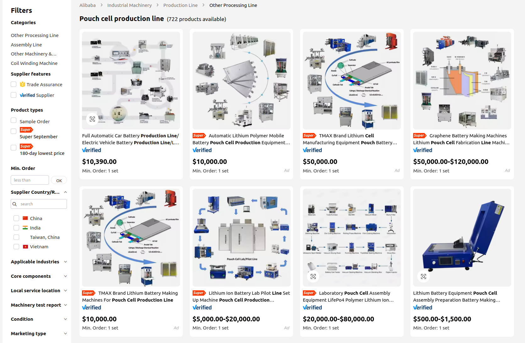
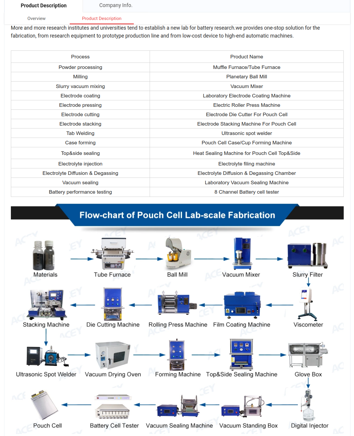
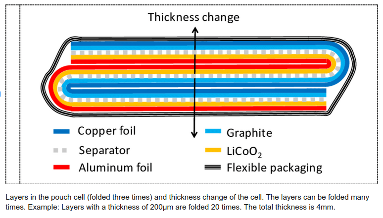
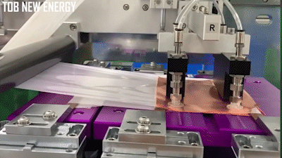

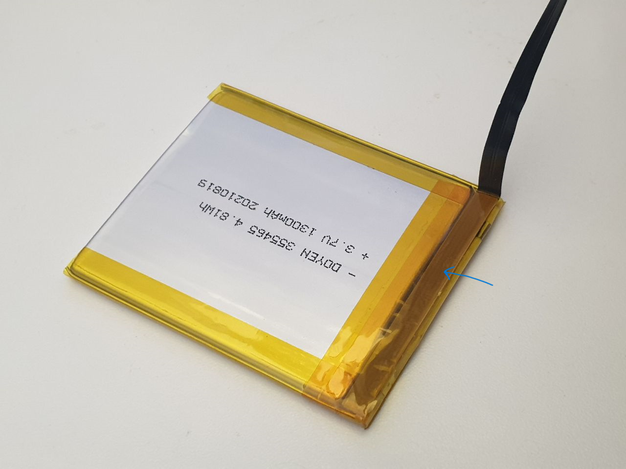
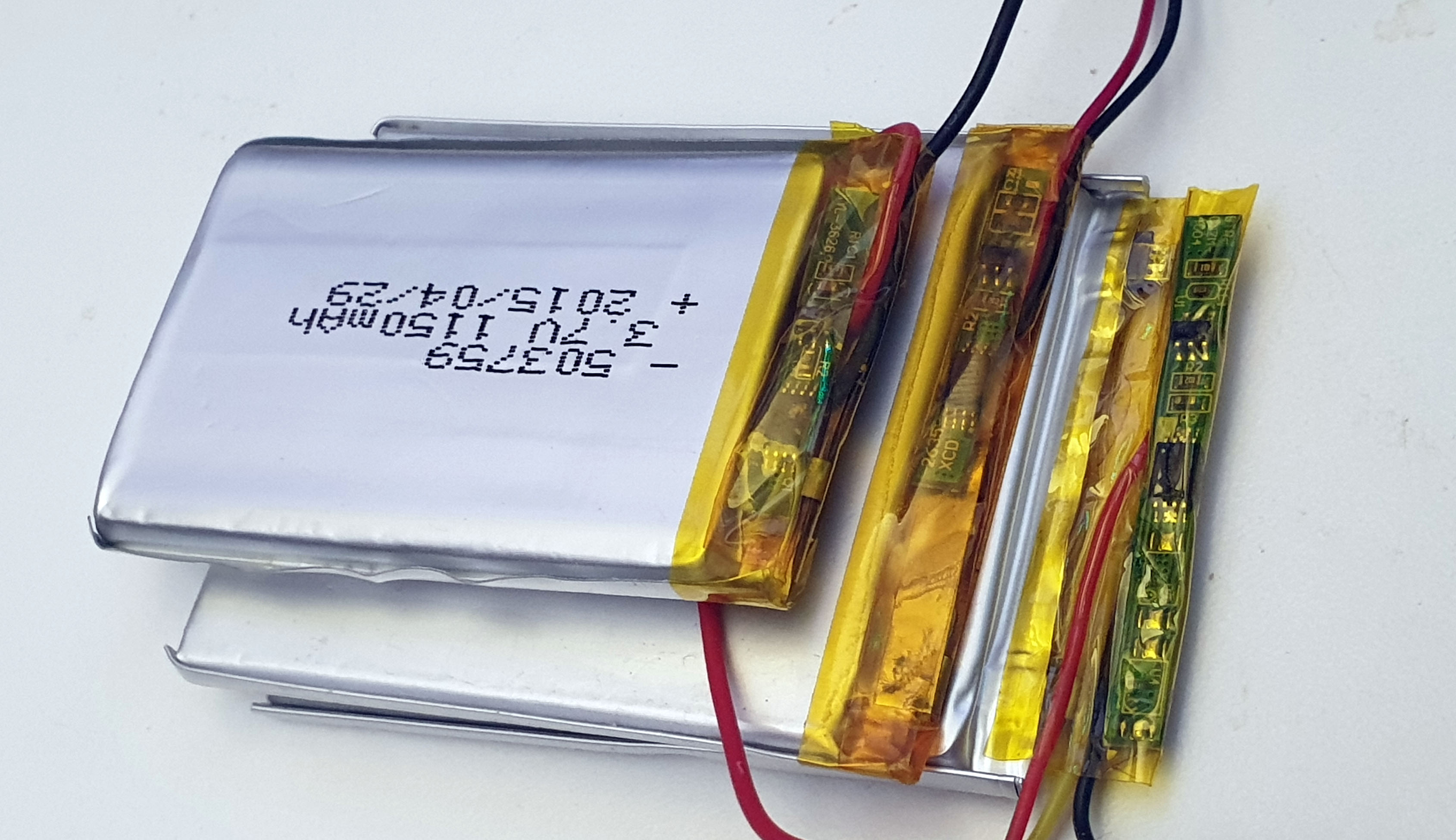
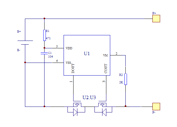
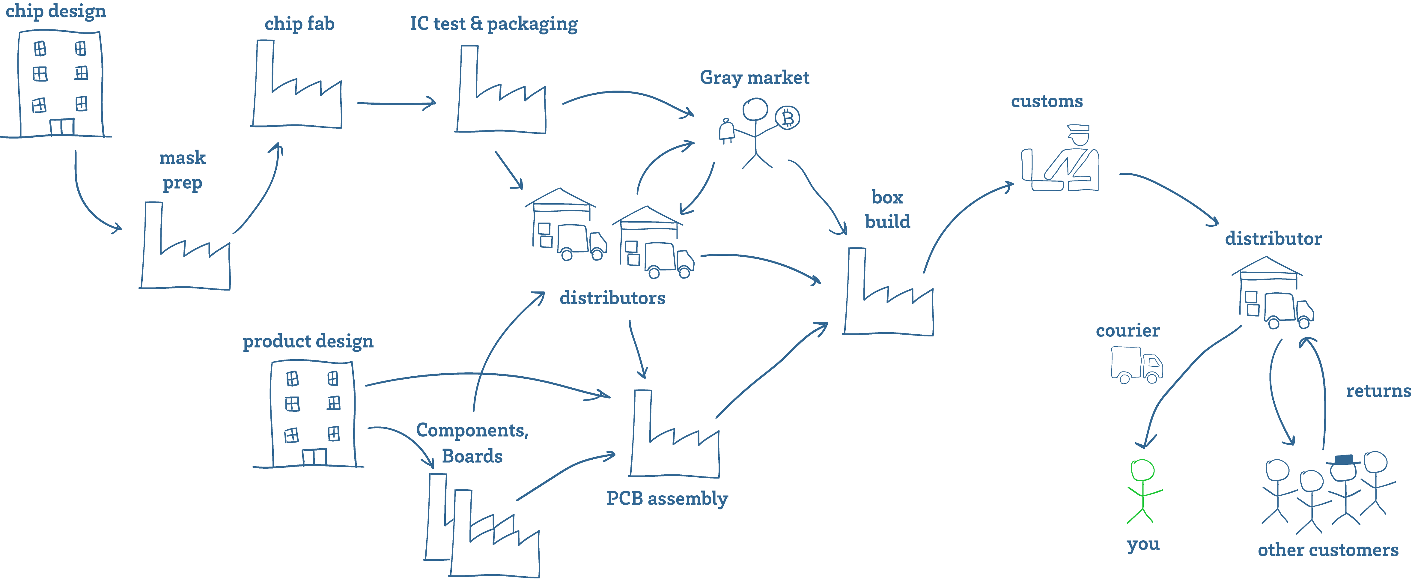
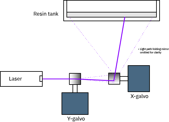
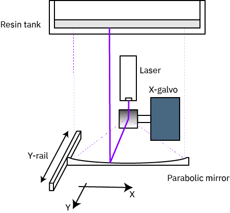
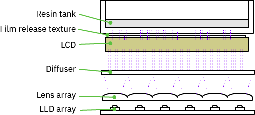
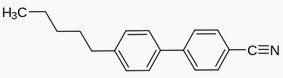


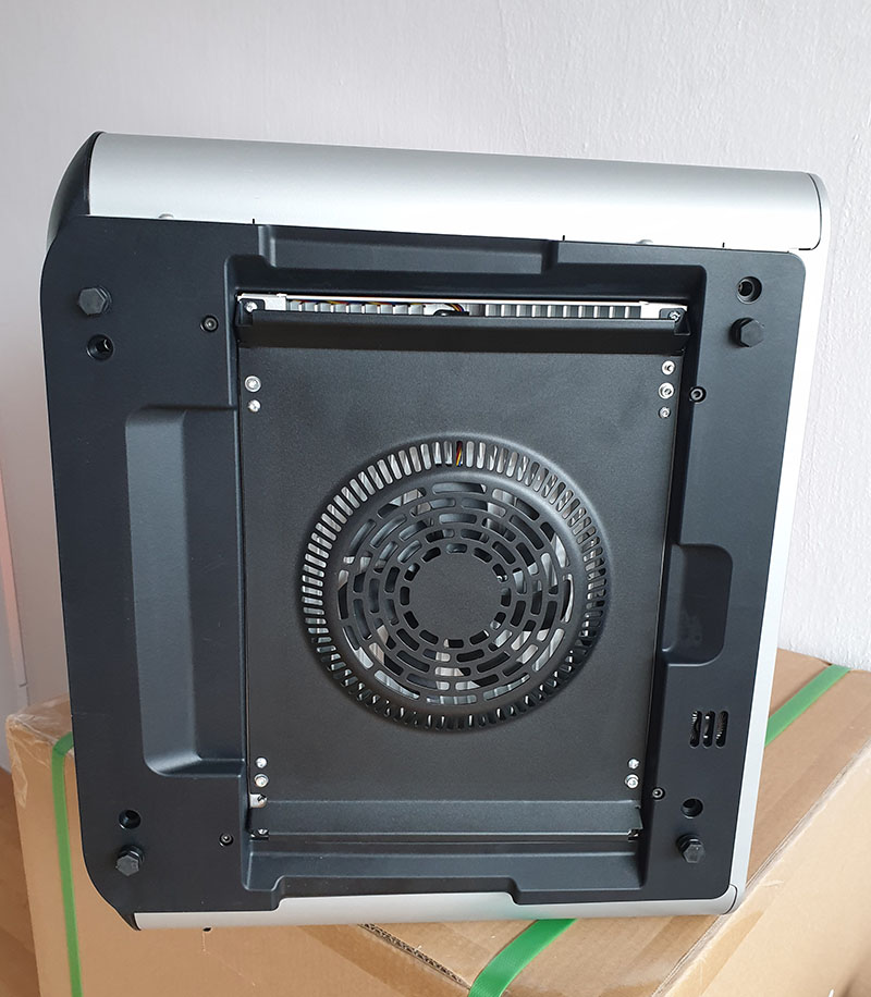
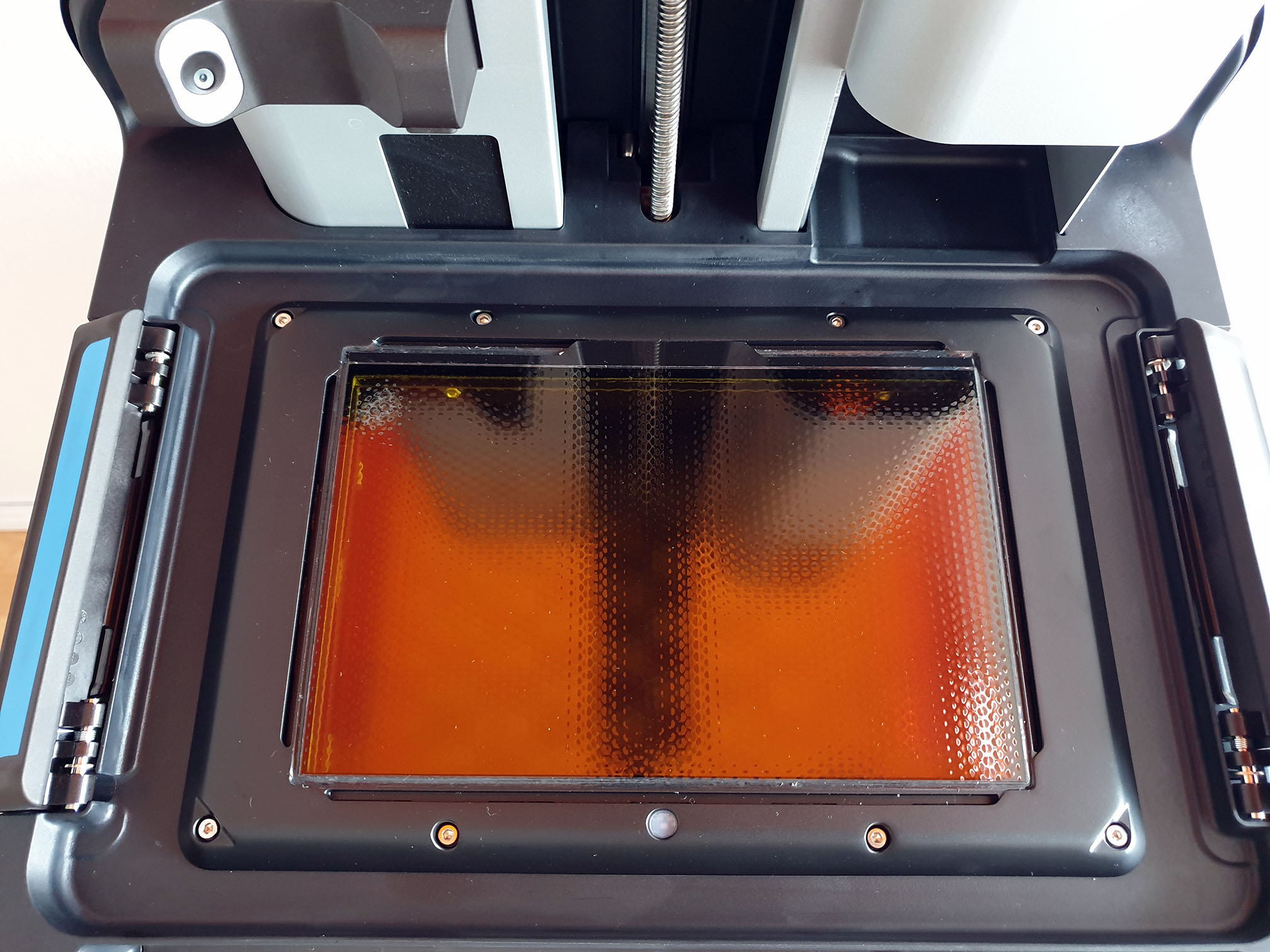
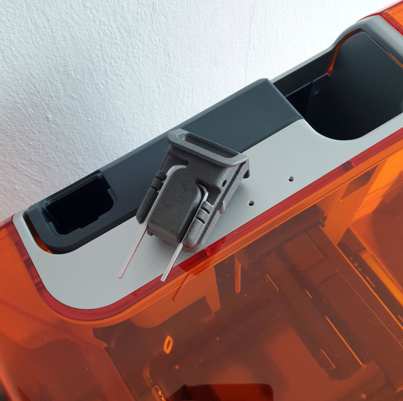
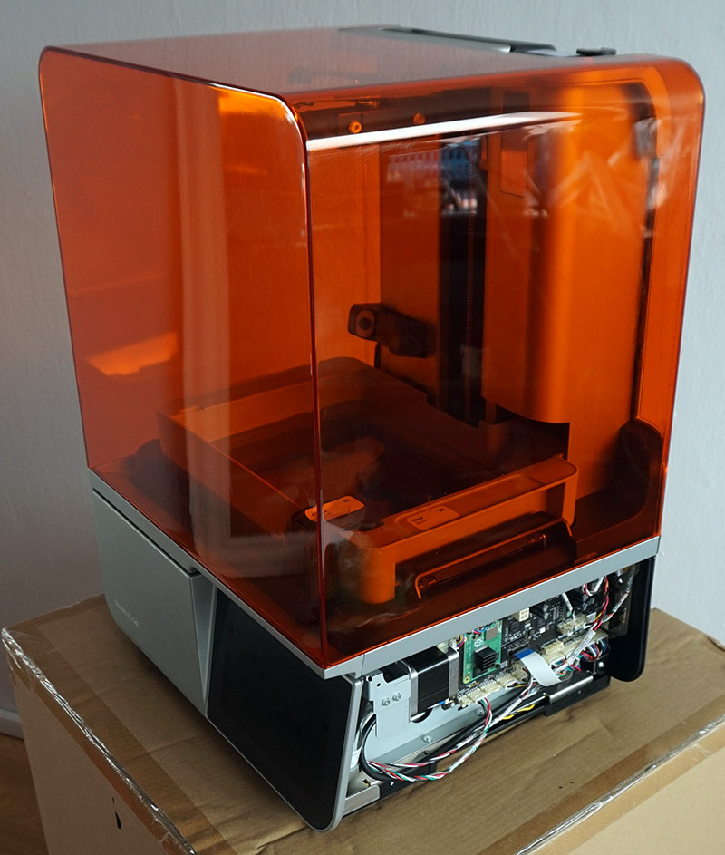
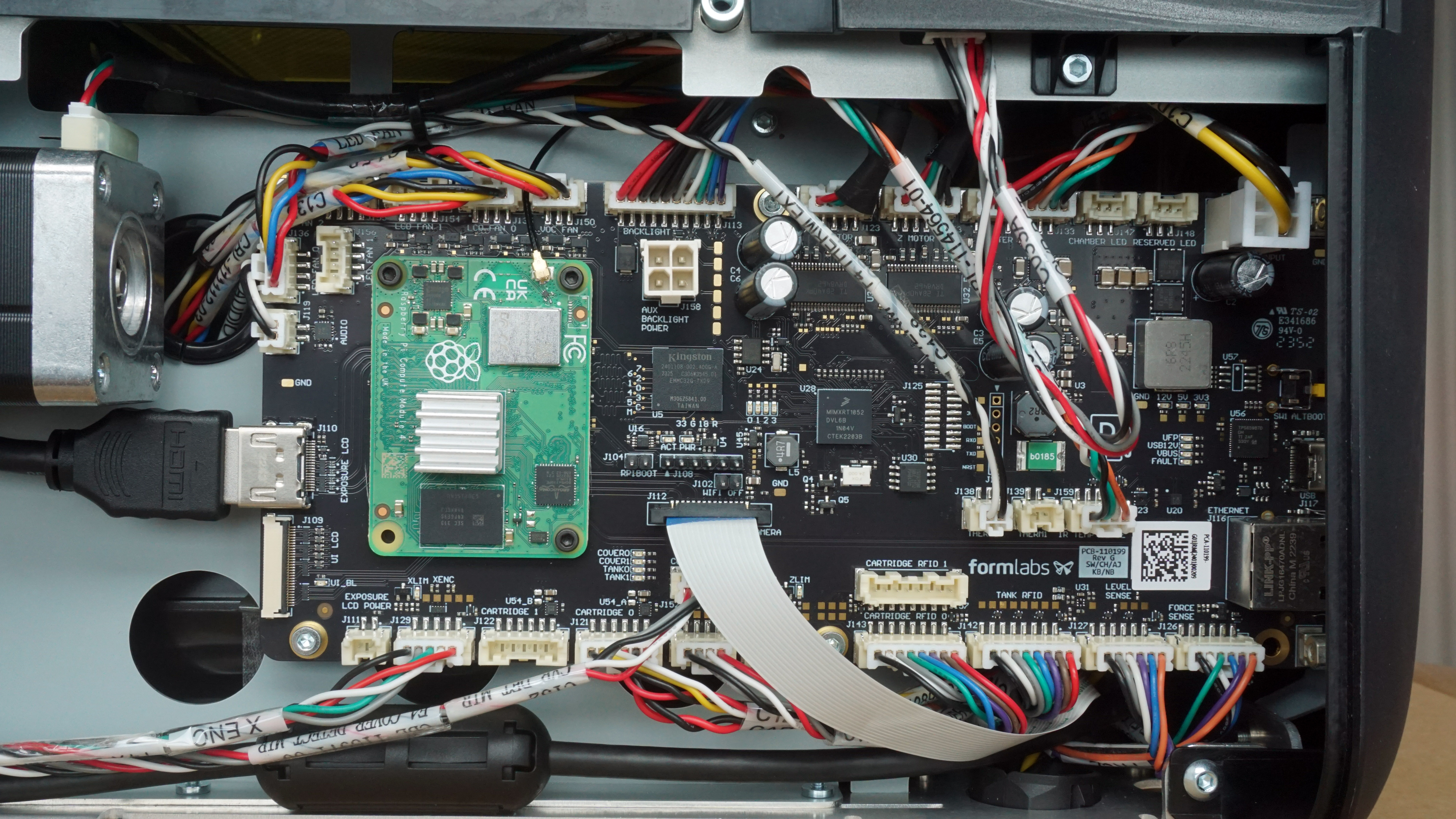
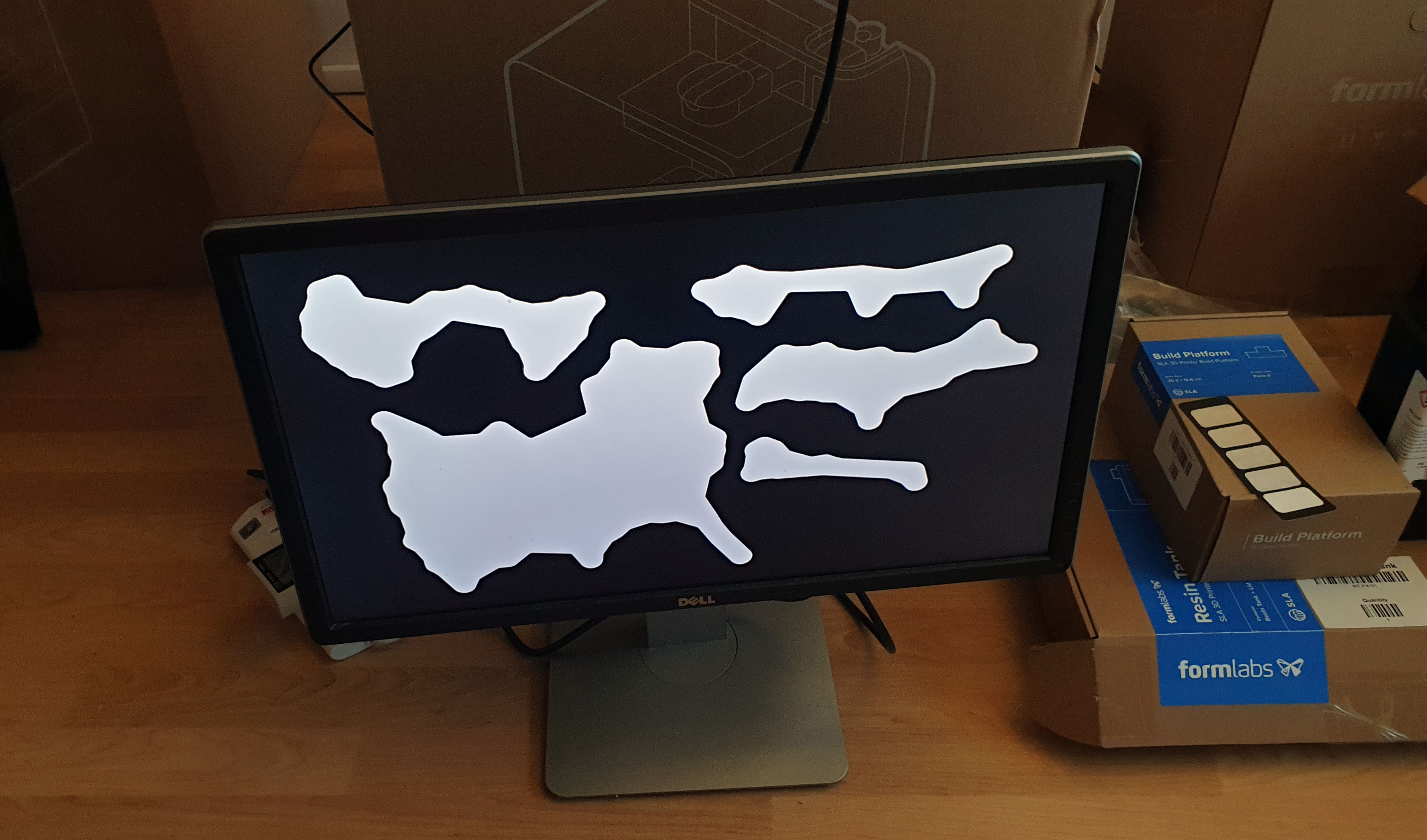
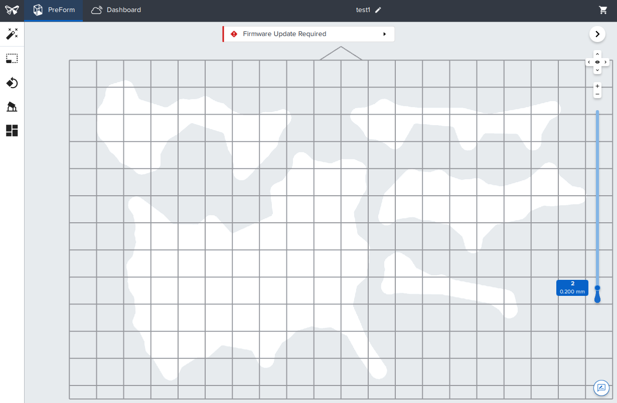
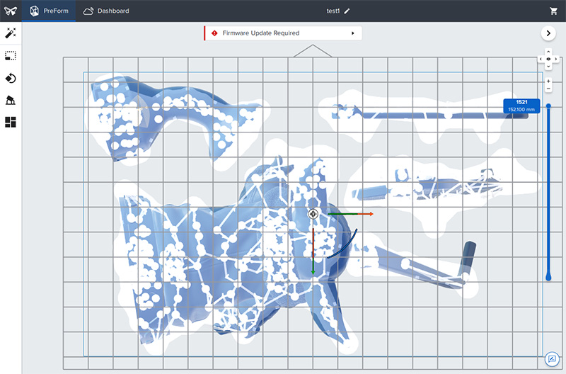
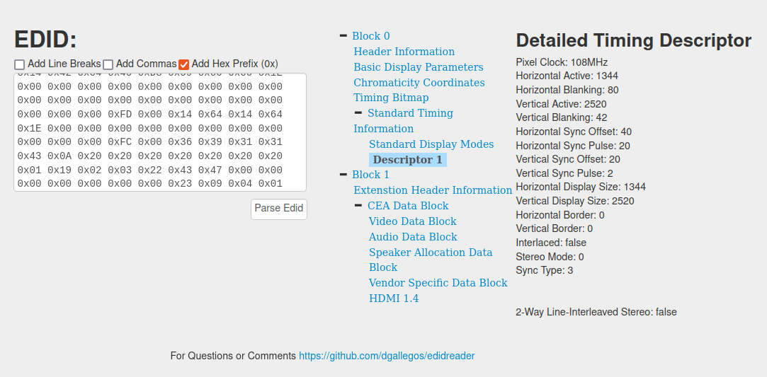
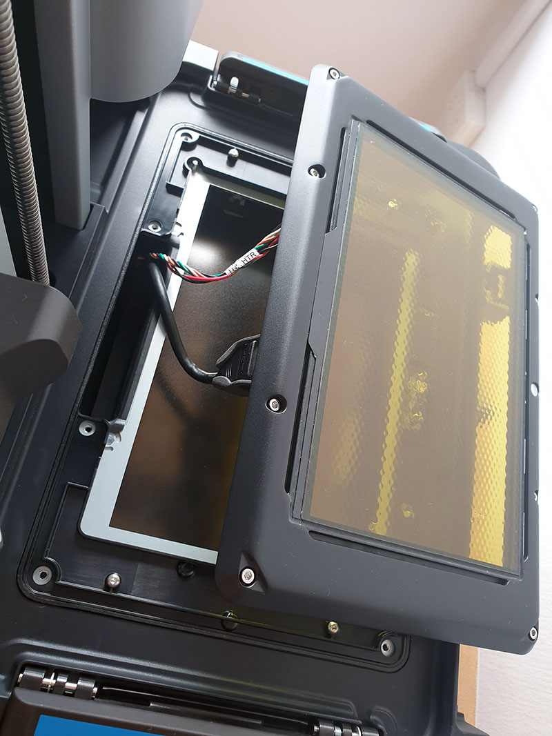
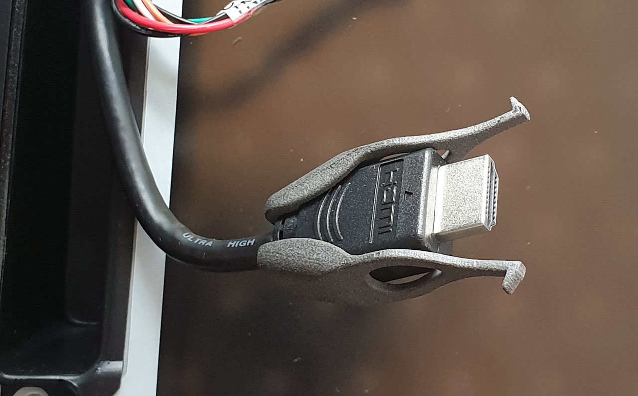
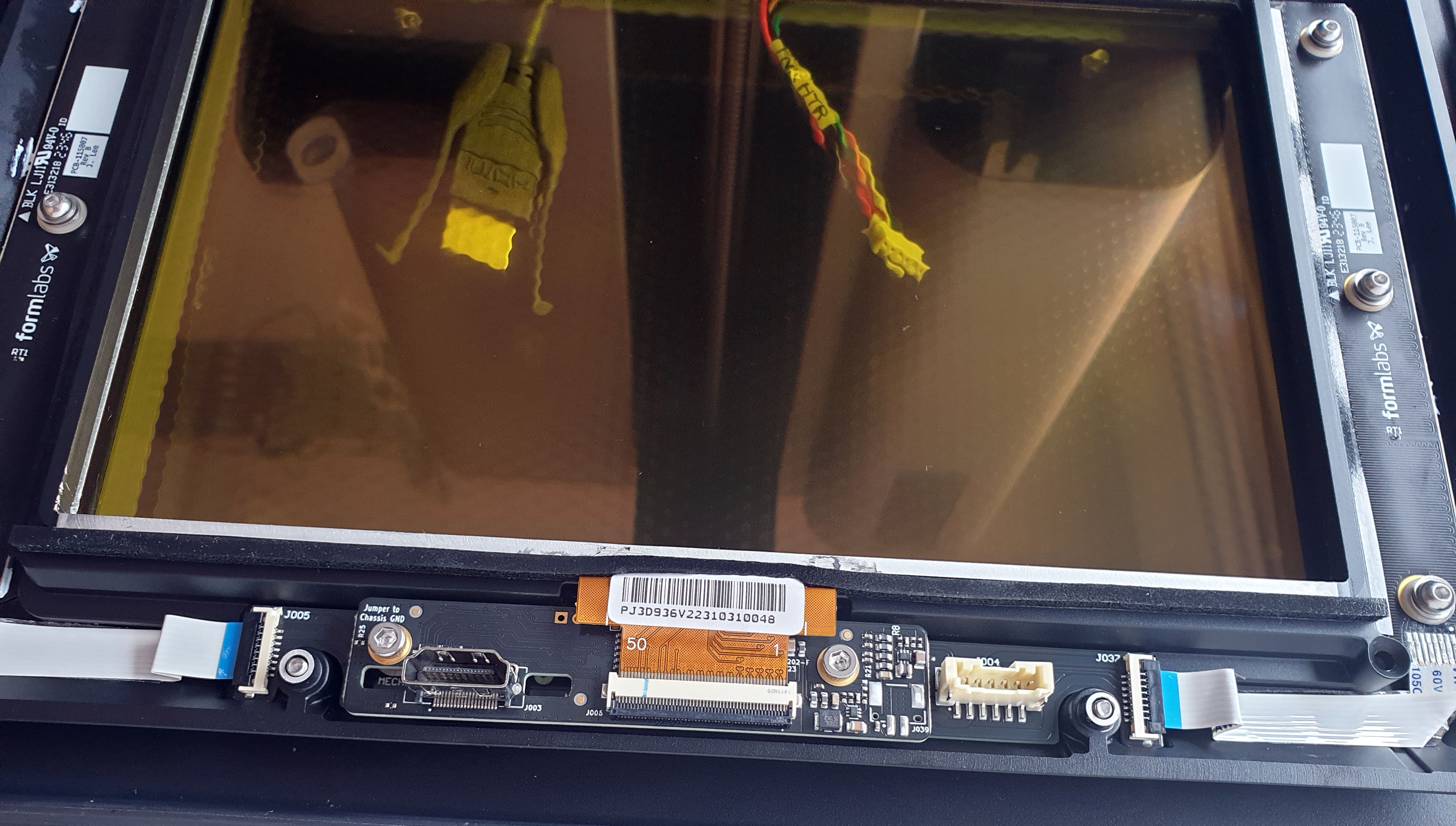
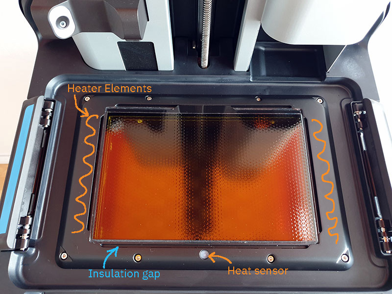
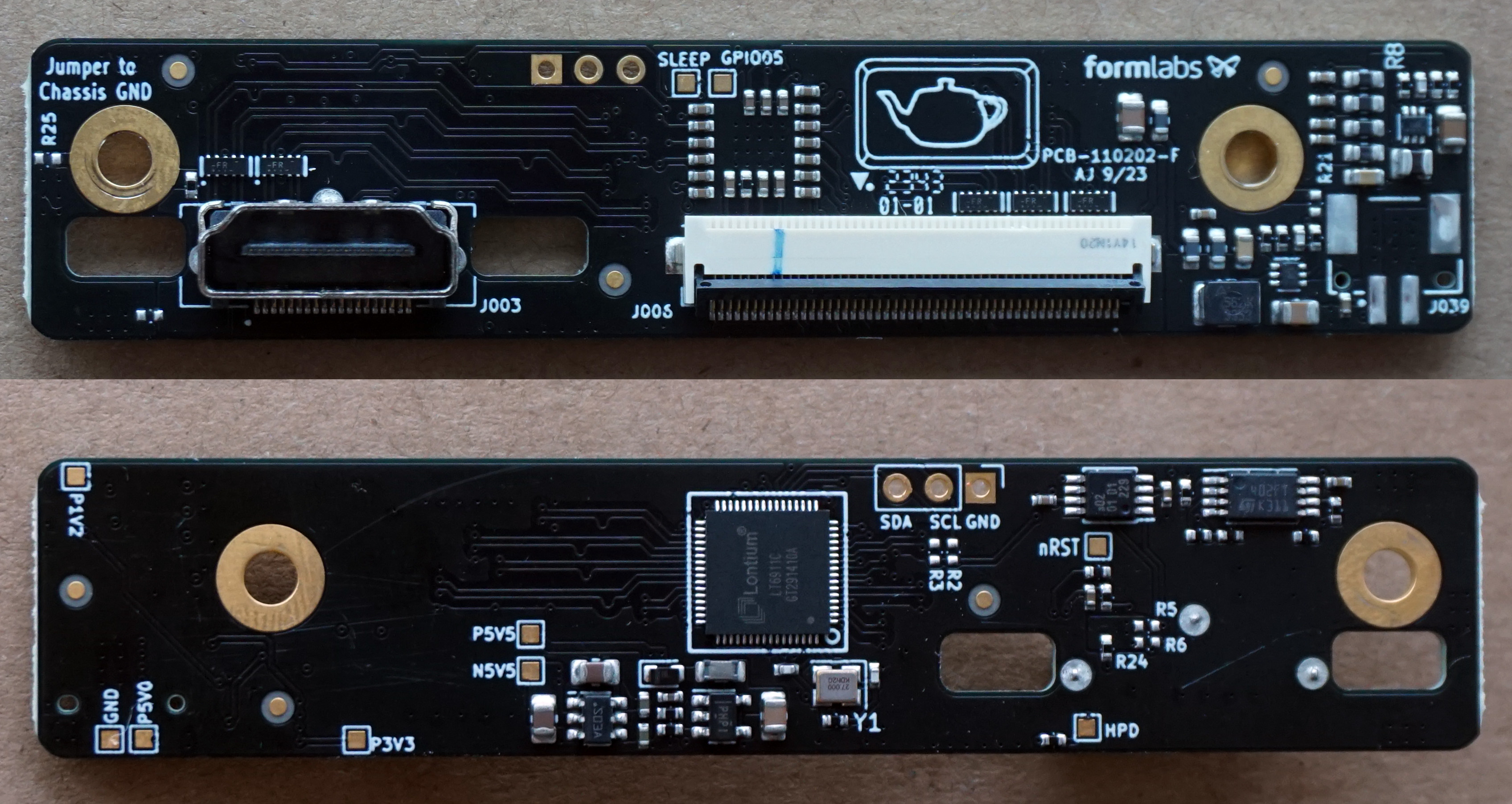
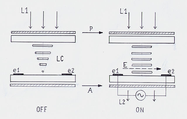
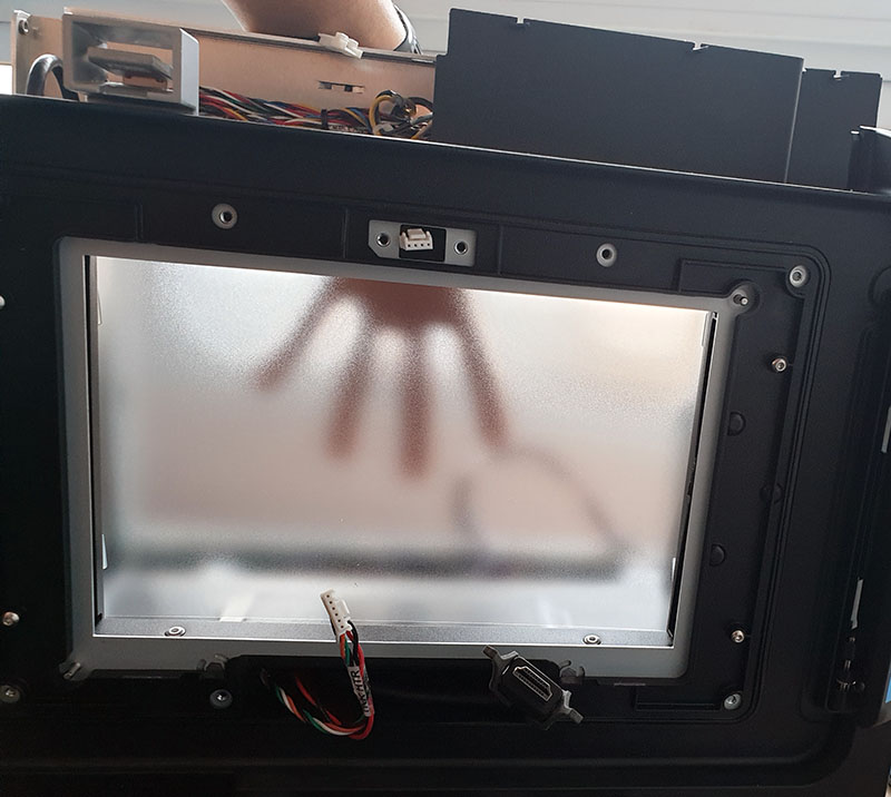
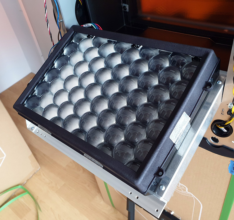

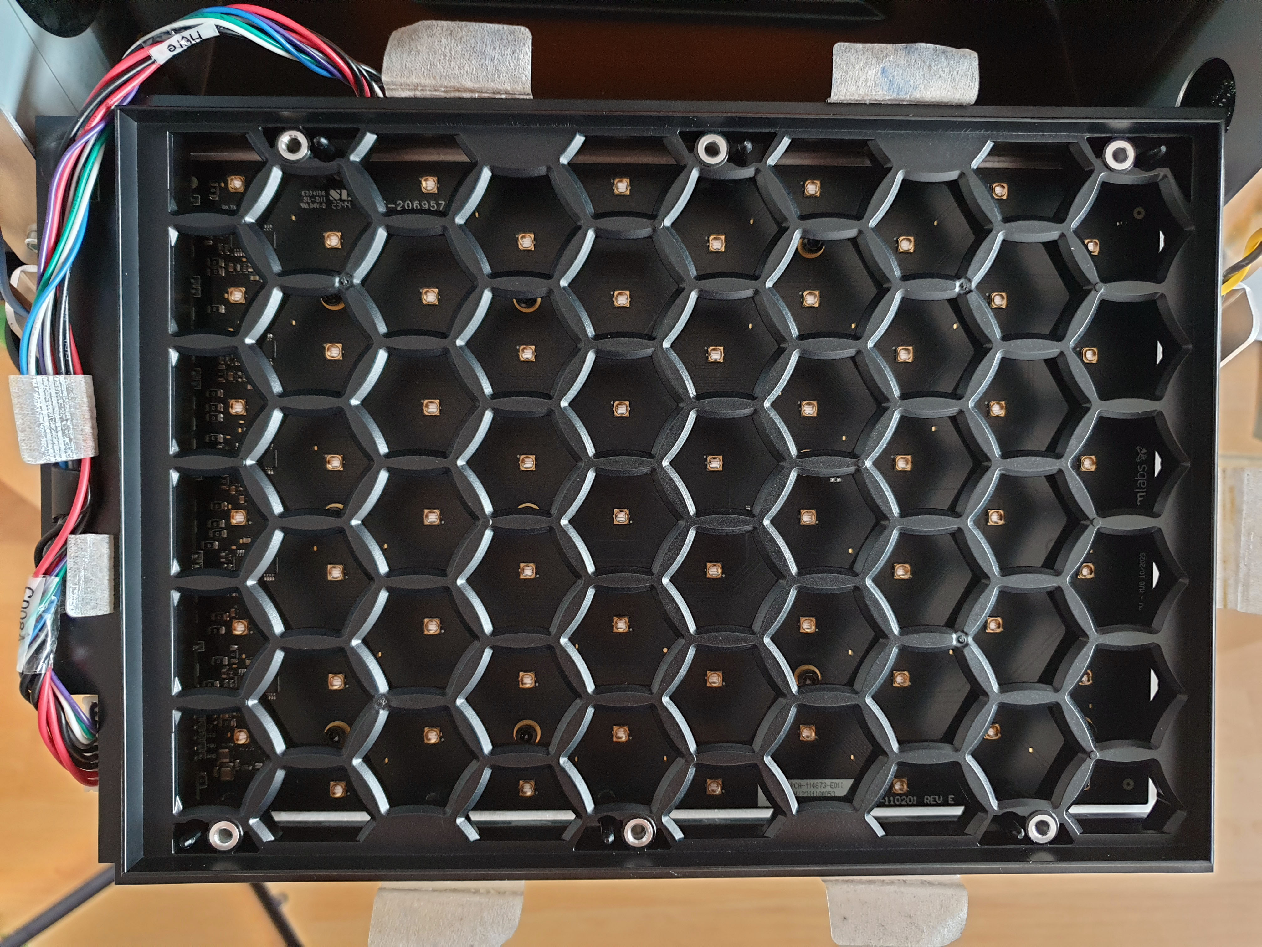
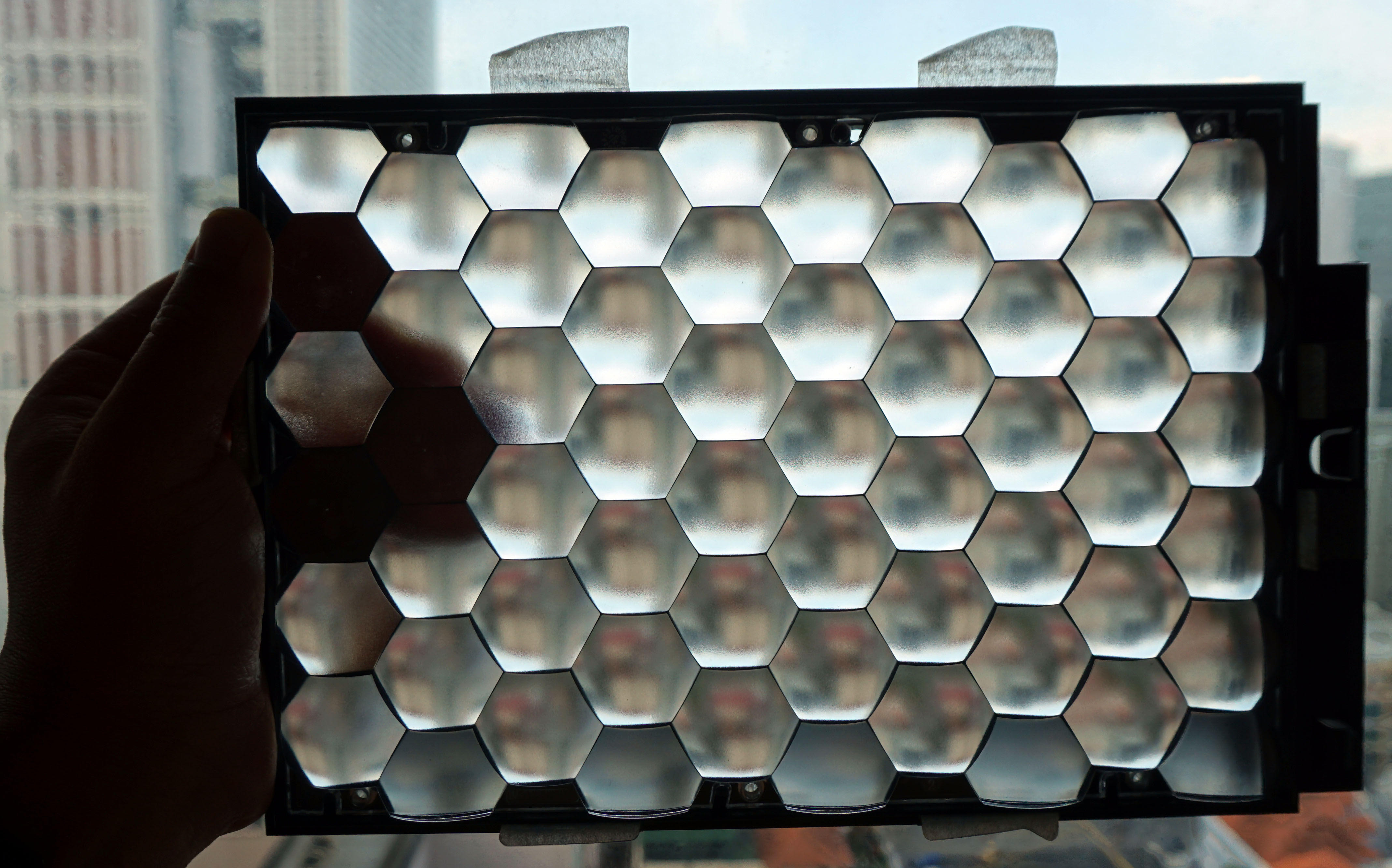
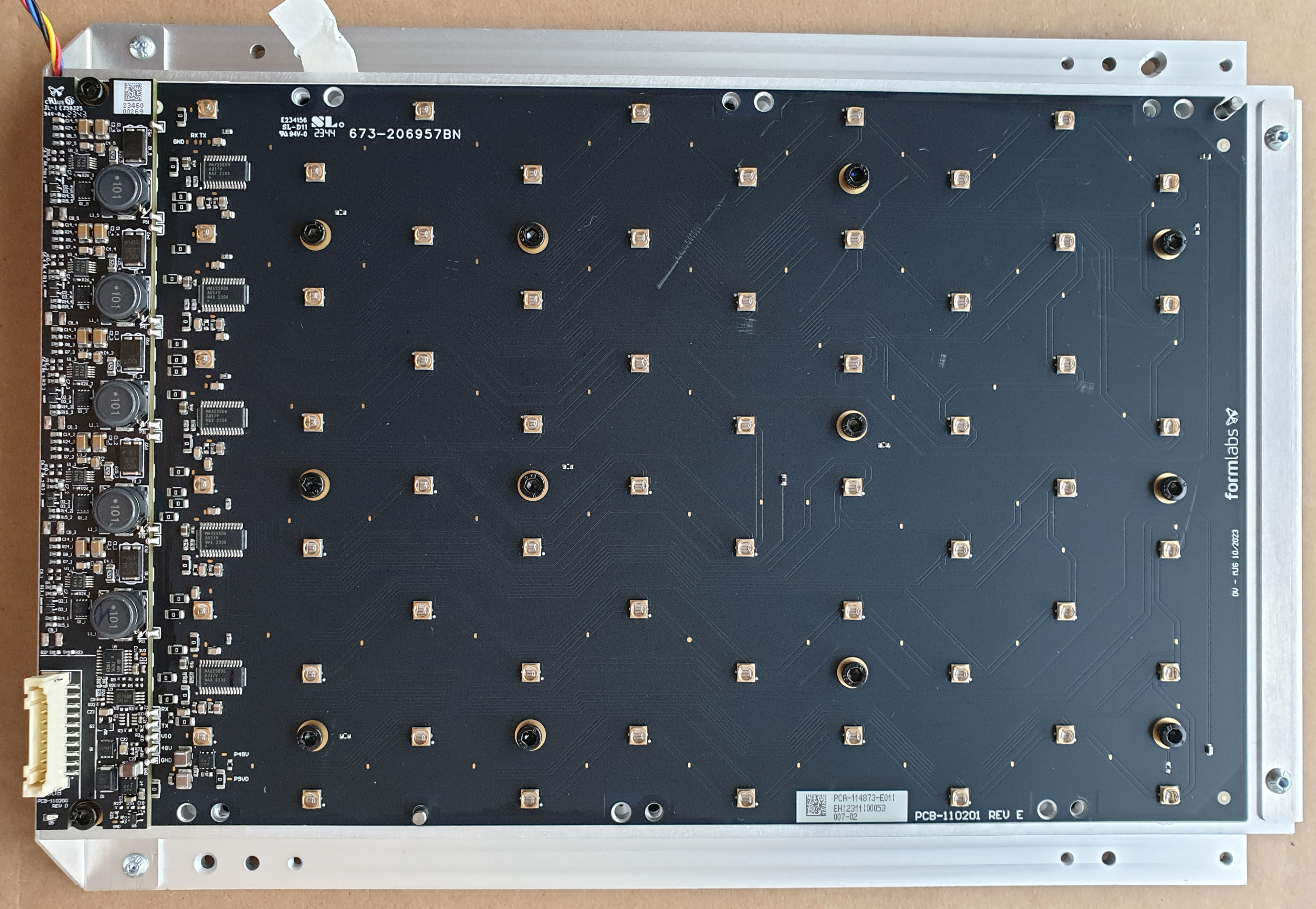

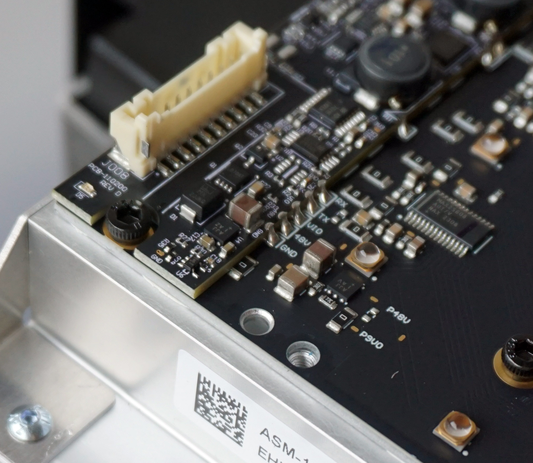
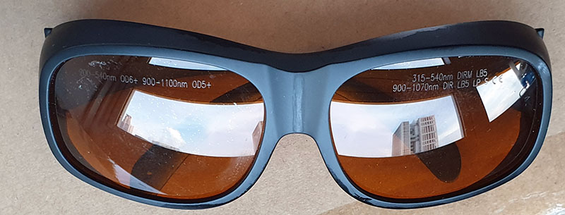
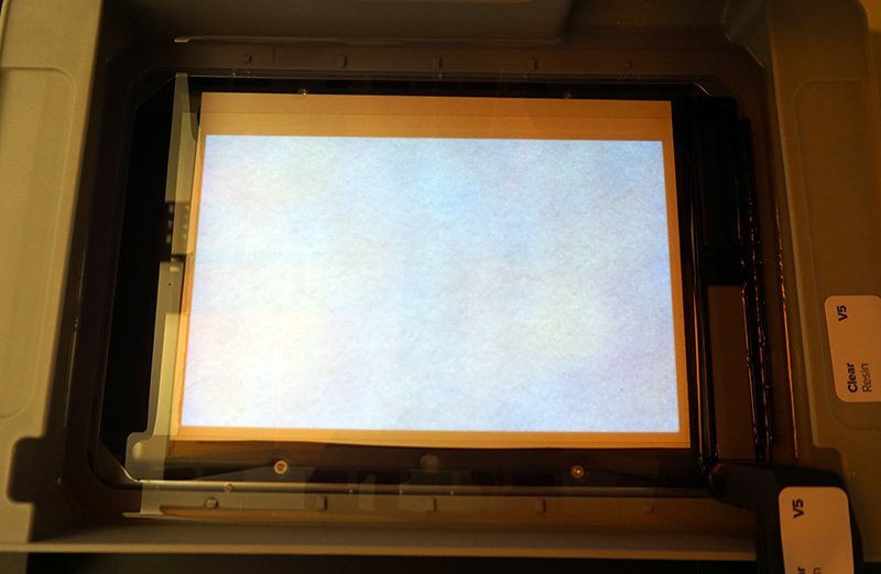
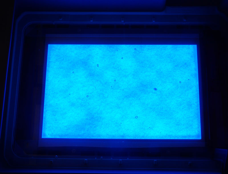


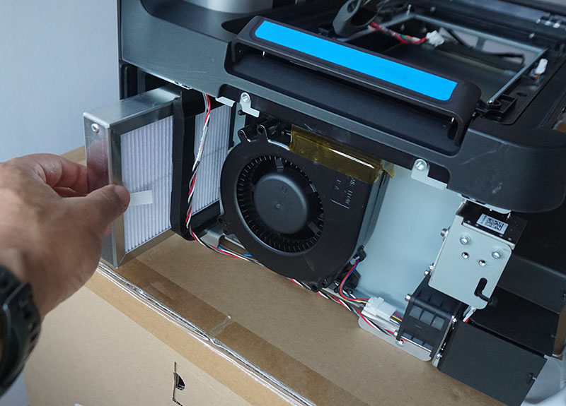
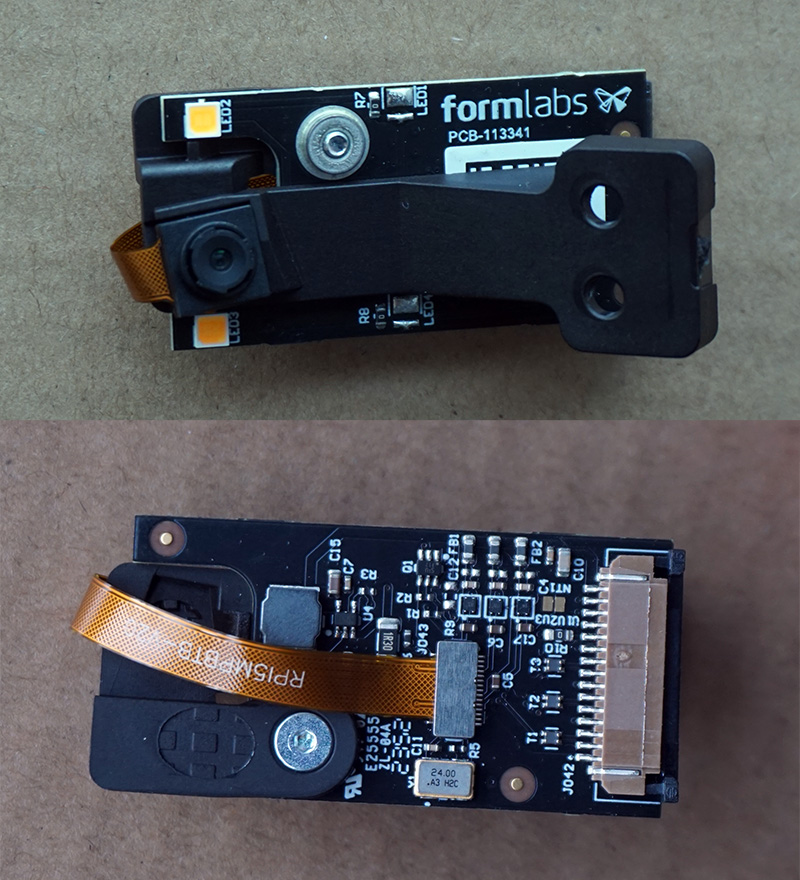
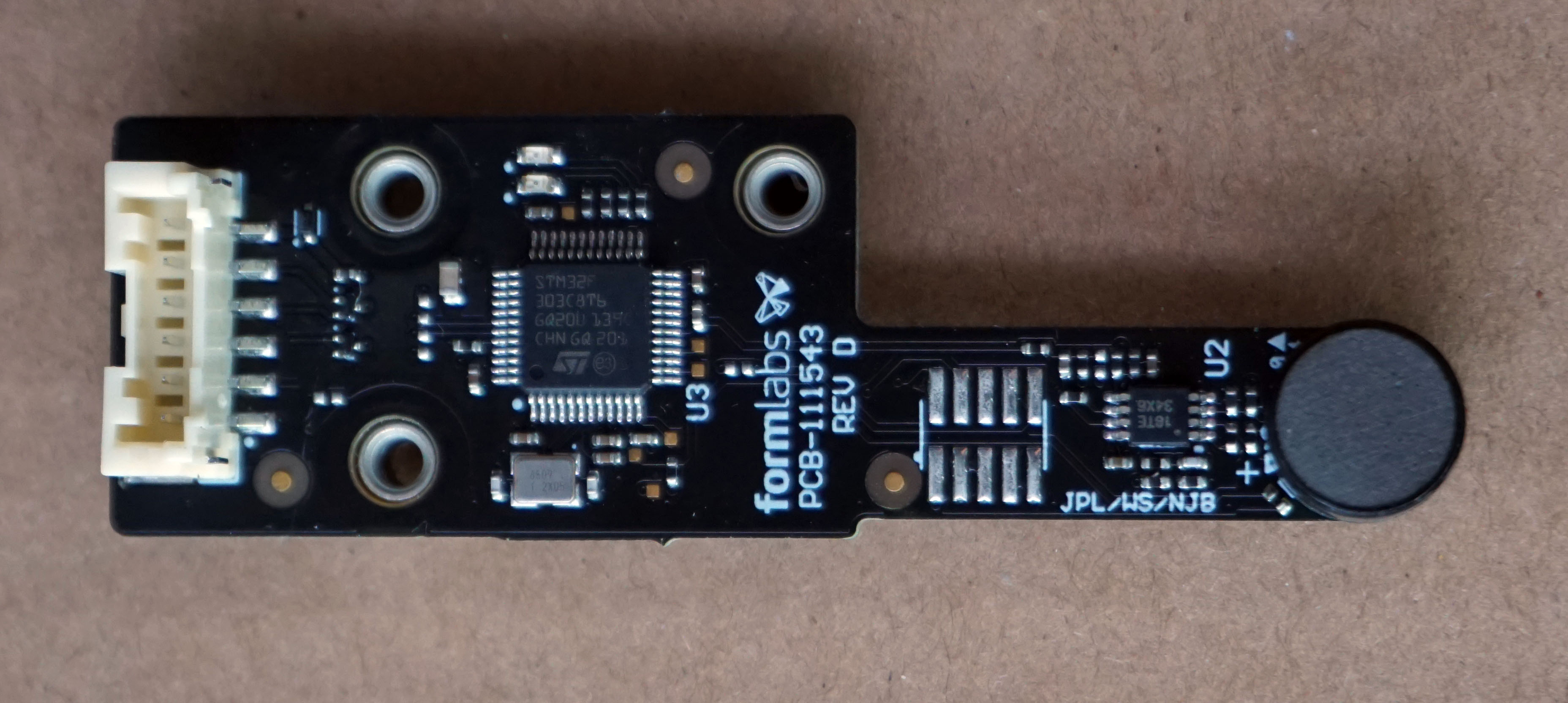
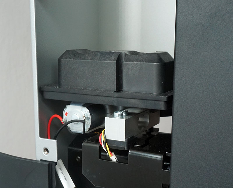
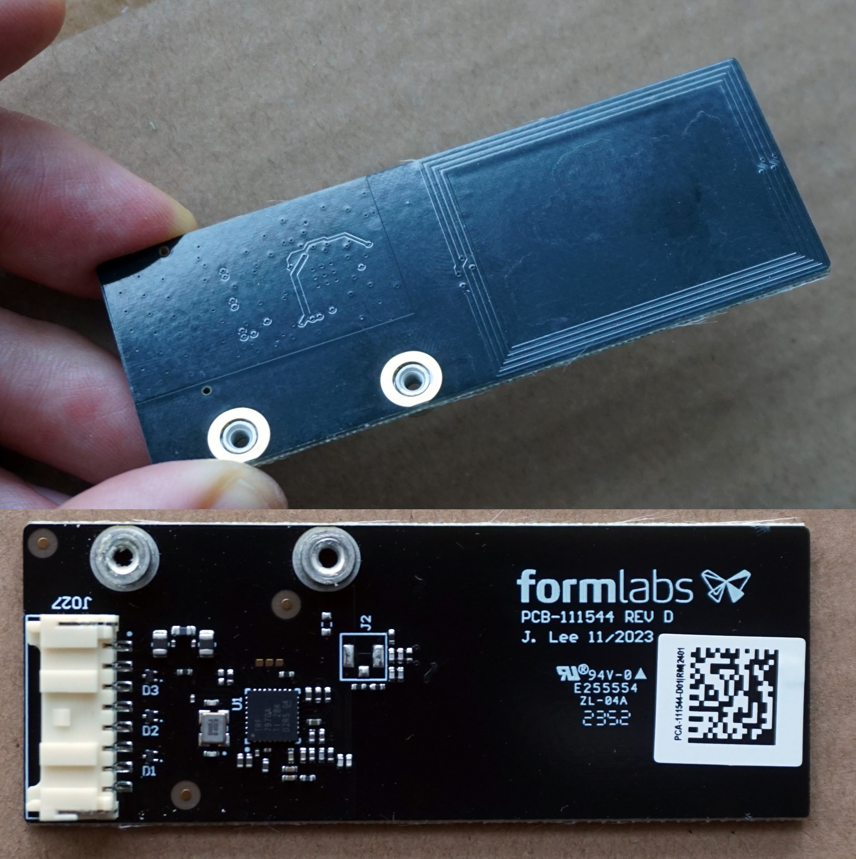
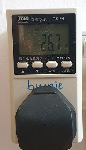

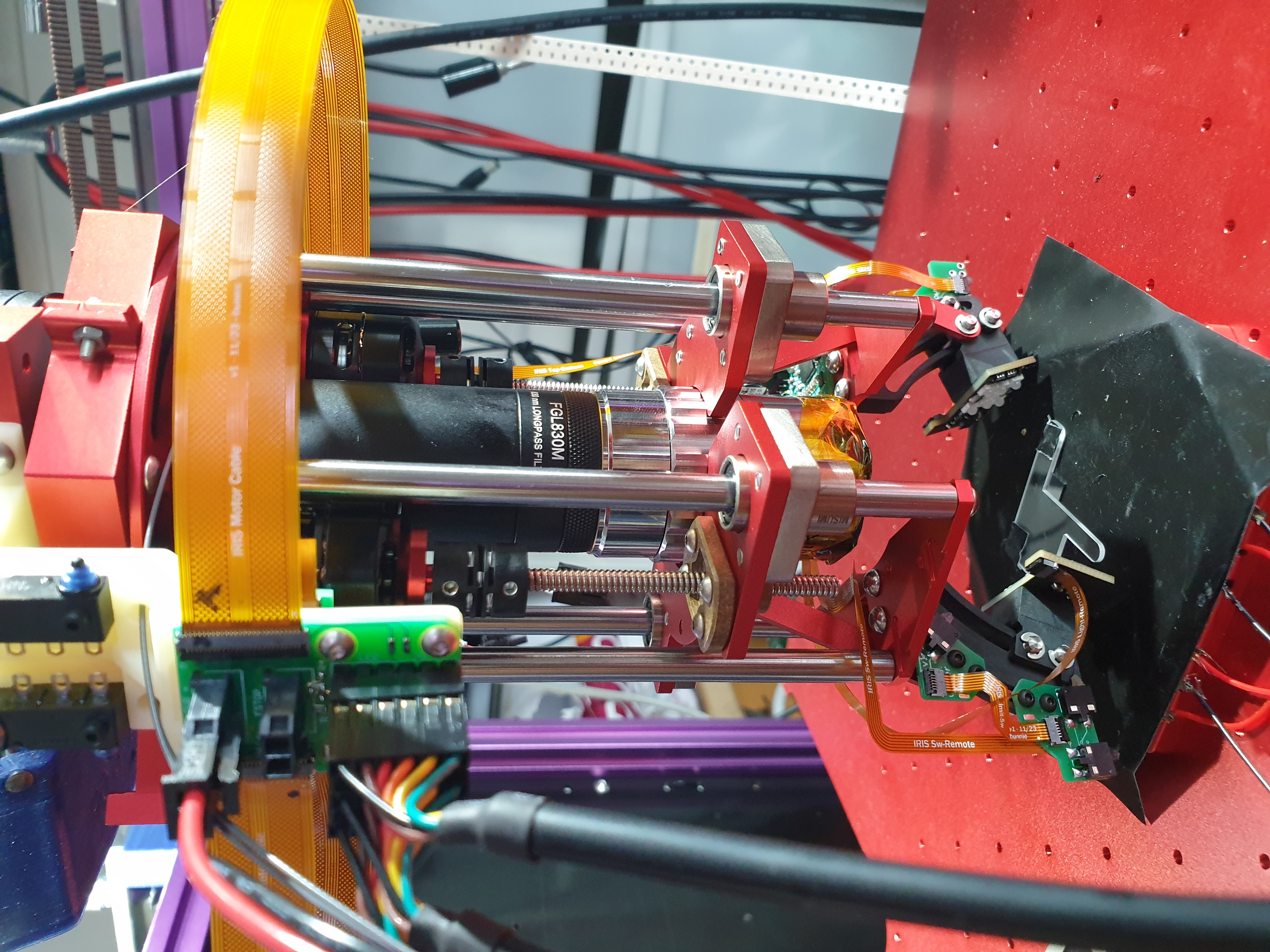
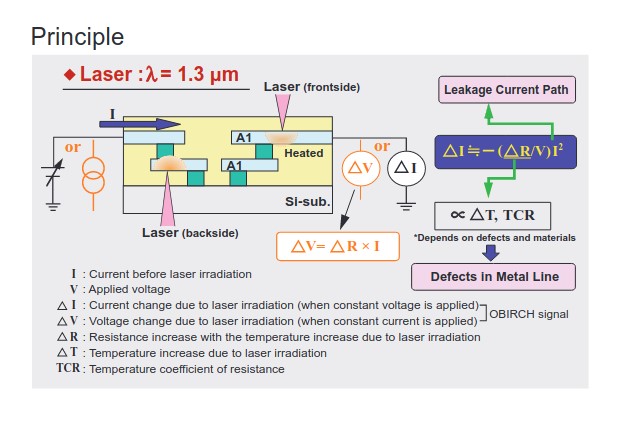

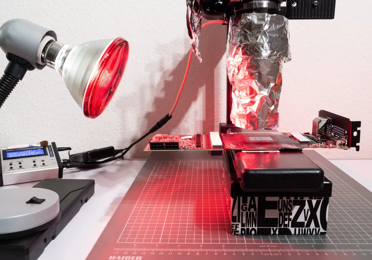
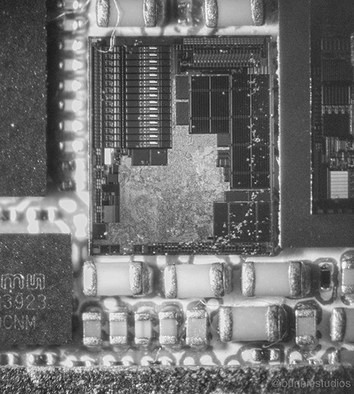
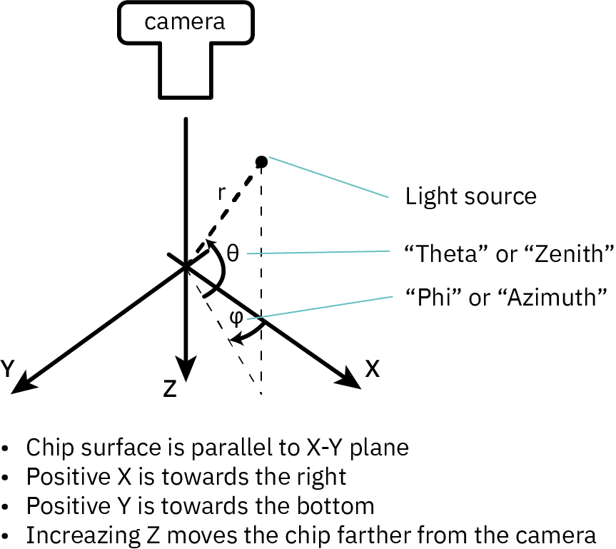
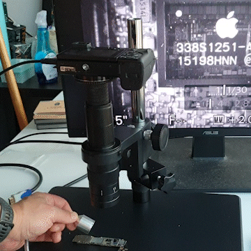

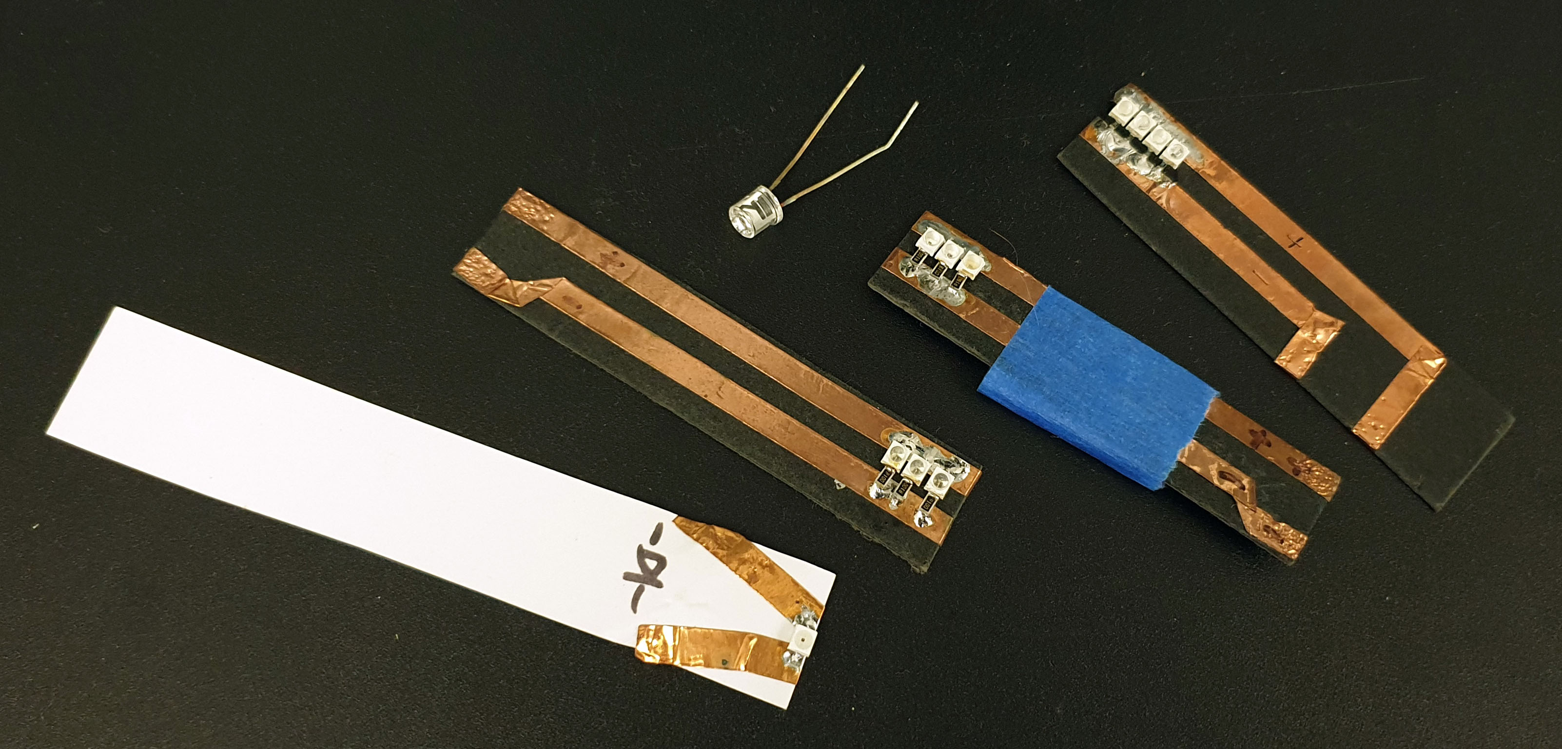
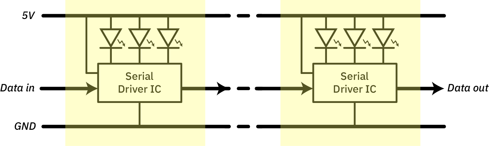
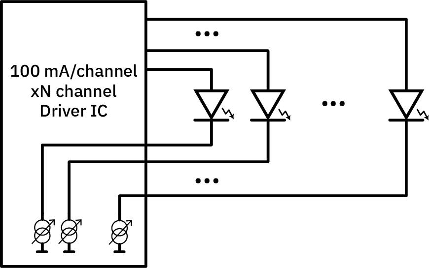
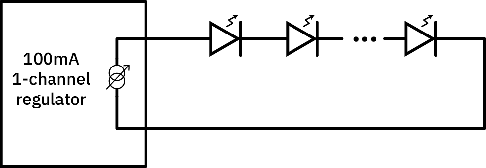
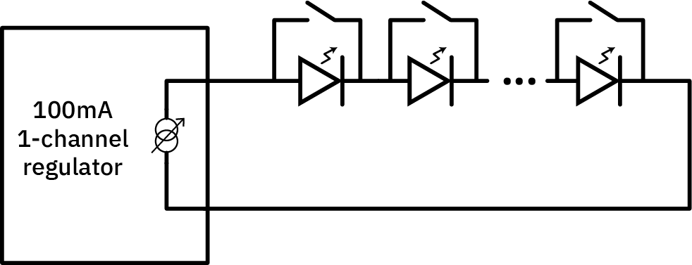
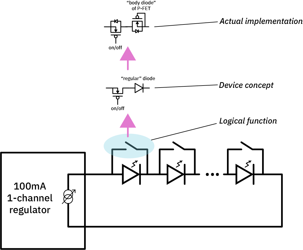
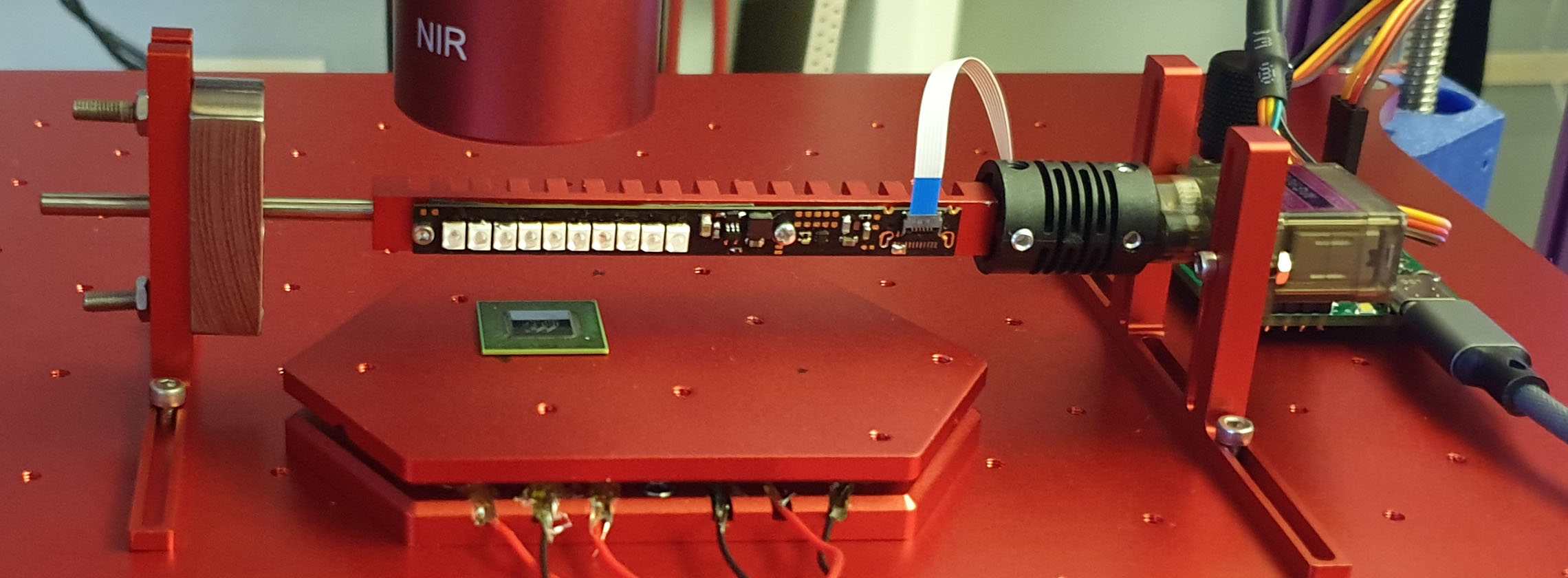
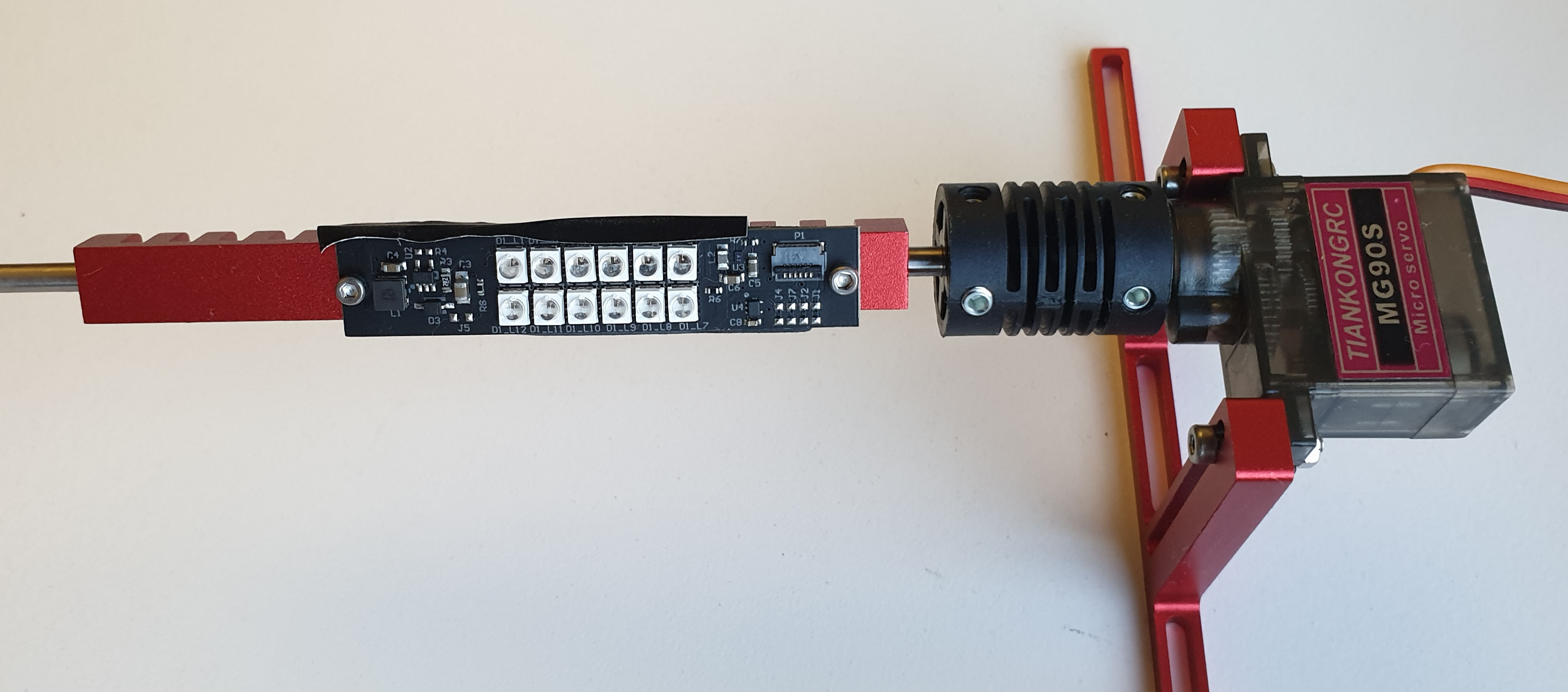


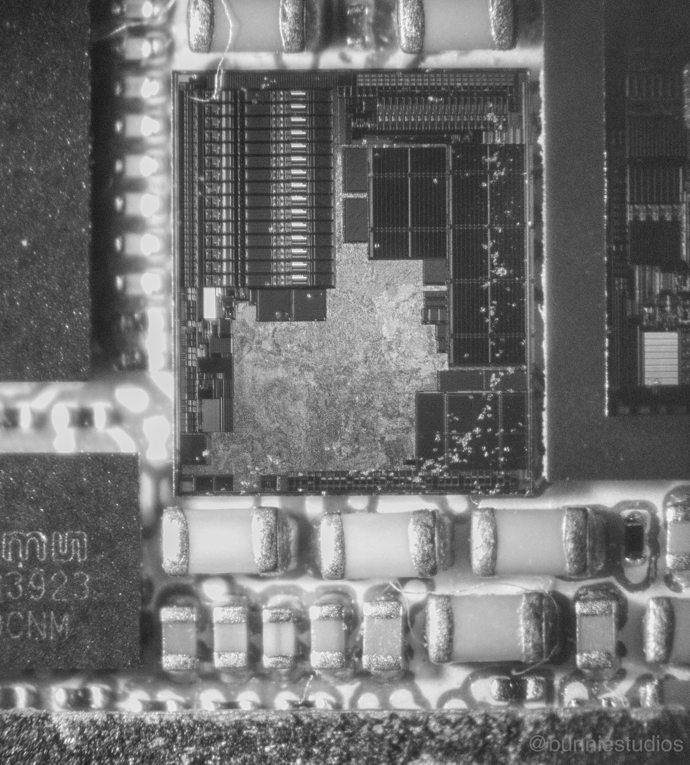
