The ware for February 2008 is shown below. Click on any of the images for a larger version.

The past two Name that Wares were fairly easy, so I thought I’d make this one a little more challenging — and yes, this month I can offer again a dent-and-scratch chumby as the prize! This one involves silicon reading — for those unfamiliar with the art of reading silicon, check out May 2006’s name that ware and the primer post (has this competition really been going on for that long? I should make a picture calendar of past Name that Wares).
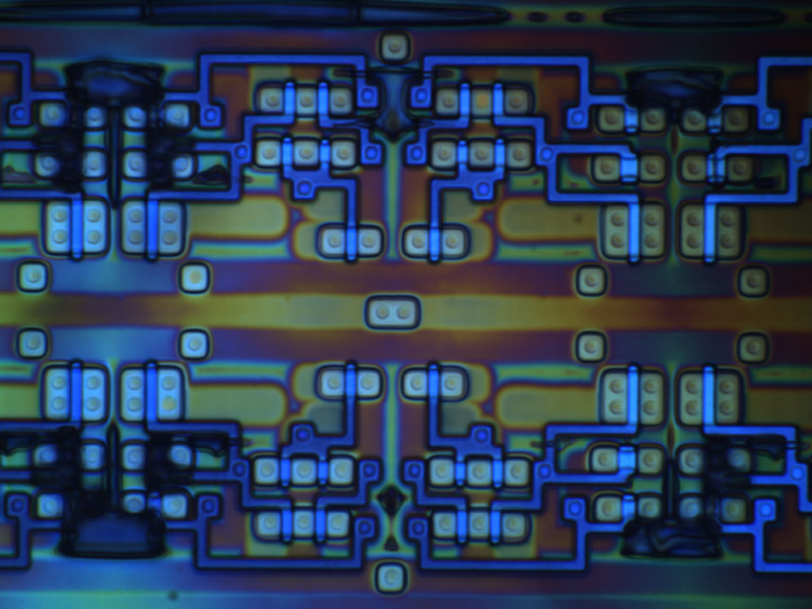
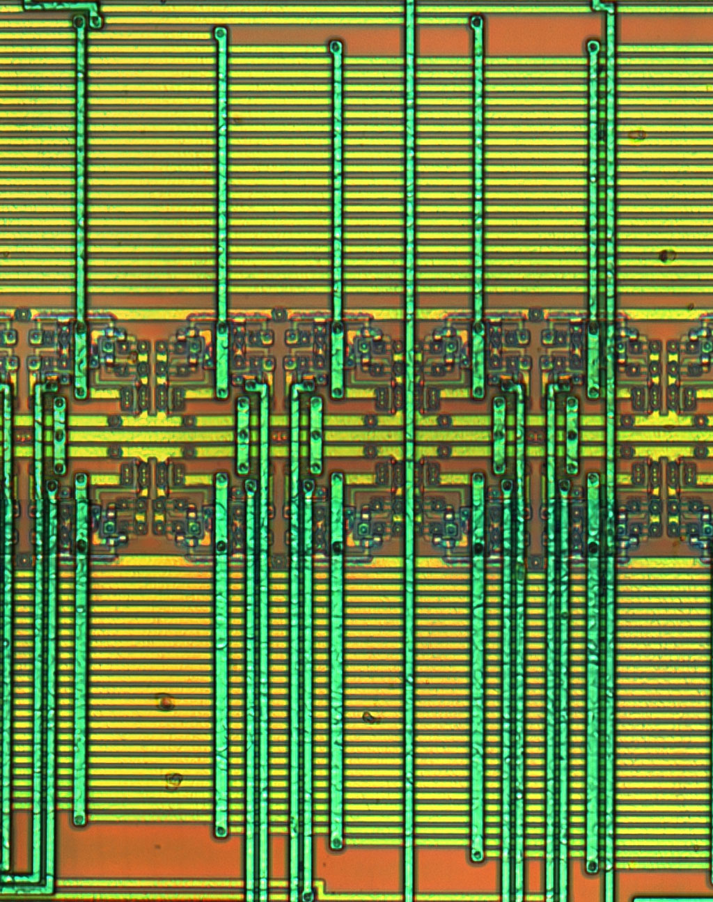
In the above photos, there is a single unit cell, replicated a few times, and the objective is to correctly name the function of the unit cell. There is sufficient information in the above micrographs to derive an exact schematic of the unit cell. The top photo is a zoomed-in version with all layers intact; the middle photo is a confocal image of the unit cells with all metal stripped back, revealing just the polysilicon gates. The bottom photos is an all-metal intact context photo for the unit cells. The photos are, as usual, decaped, delayered, and imaged by the skilled hands at Flylogic!
What I can get while staring at the picture for about one hour :-)… When using the 3rd/overview picture for describing the gates, here’s what I found out:
The 3rd picture is showing roughly 5.5 times 2 cells. Each cell consists of 8 transistors. The vertical connects in the upper half are outputs, as are their mirrored counterparts going down, obviously. The remaining vertical connects to the cells are inputs.
There are 5 horizontal busses that are connected identically to all cells, the three in the middle and the ones just adjacent to the top of the upper and the bottom of the lower cells. The outer lines (top, bottom) are GND, the inner ones are Vcc and a third signal going to all cells, but I’m not completely sure about the correct permutation of (GND, Vcc, X).
So my guess for this is, that the unit-cell is a…
chris@evil [~] $ echo “my-guess-goes-here” | openssl md5 -hex
30d5bfa53e3b8b0049033255e5fab85d
Aaaaargs. Did not want to submit that fast. So here goes some additional information. First note: The 1st and 2nd photographs are offset by about 50%!
Why is the vertical metal going upwards in the upper half a output?
– If you look at the two fingers going outerward from the next-to-center horizontal bus-lines, you’ll see that they are the source terminal of the bigger transistor that look like a lego 2×2-brick. The Lego-brick transistor forms a inverter with the one you get to, when following it’s gate (in the 2nd picture, just go straight over the via). The drains are both connected to the up-going metal.
– Why are the lines with the fingers going outoward Vcc?
They do not only go to the source of the Lego-transistor but also to two additional ones, so my guess is: Many sources -> Vcc or GND. The LEGO transistor is big -> p-Channel -> Vcc.
– Where’s GND?
That’s the trace just on top of the upper, and below the lower row of cells. There are fingers going inward to 4 parallel transistors (the one that look like O|O|O) in the middle of the 2nd photograph. The middle O is GND.
– Why are the downward only lines inputs?
They go to gate-terminals. It’s the via in the “bent-fork” shaped gate structure in the middle of the 2nd photograph.
I’m going to say it’s a row/column selector.
– Why?
Because I notice only one signal/trace between the sets of cells as an input to the cell. I figure the signals/traces on the outside of the cells to be the outputs.
If you look at the vertical traces (perhaps metal layer 2?), you see they are not coupled together at all. So it appears each cell can be selected independently by the vertical metal-2. Horizontally it appears to be a row select.
Okay, I have my update. I went through and just did the rough sketch and layed out all the poly, metal, contacts, and diffusions in stick diagram form, and I’m claiming it to be a demultiplexer.
Sorry this is not a guess to the Name That Ware, but I thought the smart people here might be able to point me in the right direction for a ware of my own…
I have media player that has a voice recording feature, however, my work does not allow any kind of recording device on the premises, so I’d like to remove the microphone.
Problem is, I’m not sure what it looks like! I took the cover off, but most of the circuit is behind a battery. The battery is stuck on to the ICs via some thick spongy tape. I tried prying it off, but its stuck pretty good.
Anyways, can anyone tell from the picture which one the microphone is? I figure it should probably be close to the card connector opening so that it can pick up sound more easily, but the only thing that doesnt look like a resistor/ic is this silo looking thing that has the letters “YDF” on it, and is located on the lower right of the blurry picture.
Also, is theres a easier way to disable the microphone that trying to desolder it?
http://i28.tinypic.com/2nqa74i.jpg
Thanks a bunch!
Ben, the picture is really awful, but you are right on the “silo looking thing”.
http://commons.wikimedia.org/wiki/Image:Electret_condenser_microphone_capsules.jpg
Ben: Yes, the part in the lower right looks like a microphone. It would be easy to test that theory — just start recording and scratch it lightly.
I agree, the bottom right looks like it is the microphone. I don’t take any responsibility if it isn’t and your recorder becomes permanently unusable. You may just desolder it from the bottom side if it’s not a surface-mount component.
Each cell has two inputs: one shared between all cells, and one unique to each cell.
Each cell has one output.
If the private input is low, the output is high. If the private input is high, the output
goes low (and stays low as long as the private input is high) as soon as the shared
input goes high.
So I would classify this cell as a 2b58fc2b7640a6ef92b253f2f5929447, perhaps as
used in a 6bee9ec6e258b7971065ccf101ab3729 (echo | md5).
It worked! Thanks, everyone!
It was a bit hard to get my thick soldering tip in there but, managed to loosen the mic just a tad so that I could then wiggle the mic back and forth until its leads broke.
Woohoo!
hello
i have sonme reasons to think this is the rom for config bits of a microcontroller.
as the structures are unsymmetric, unlike normal cmos circuits (or should i say “uncomplementary” ?), there are probably some hidden effects for letting some transistors conduct, eg a floating gate.
Hi,
This is my first try at reading silicon, here it goes.
There are eight transistors in each cell. The cells have one input (A) and one output (Y). Each cell generates a complement (A-) of the input, the inverter that generates A- has a different VCC than the other transistors. A and A- are then used to control two cross connected transistors. The internal state of this cross coupling is then buffered by a bigger sized inverter this is then Y.
The three traces in the middle are VCCa-VCCb-VCCa and the trace on the other side of the cell is GND.
I must have made a mistake tracing this because the schematic makes no sense to me. When A changes state it will have a PMOS and NMOS on at the same time in the same serial connection (momentarily).
Well, here is the MD5 of my schematic, unfortunately I can’t say what the cell actually does.
3FE21211F8E70E9A16A559F3E5B6175C
hello
finally, i think it is a b1300517e800200afe4c13c513a9847f
my schematic analysis : http://f4eru.free.fr/bunnie/
( VCC and GND are probably exchanged, no functionnal impact)
Hello bunnie,
i tried to send you an email but the contacact method stated in your blog is not working anymore. (mailbox disabled;-) is there a way how to get in touch with you?
thanks
Peter