Pictures of Logic Gates in Silicon
As part of the Name that Ware June 2005 installment, I was looking around on the chip and I found the following “spare” gates.
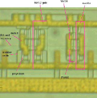
(click for a clearer image, I have to shrink images because IE breaks with large images)
I’m making a guess as to which transistors are P-type and which are N-type. There is no coloration or similar visible cue that distinguishes P-type silicon from N-type silicon. However, due to the lower mobility of holes (the majority charge carrier in P-type silicon) and therefore lower drive current per unit width, most CMOS circuit designers “balance” the P/N ratio by making the PMOS device larger. Thus, I’m guessing that the larger transistor in the inverter is a PMOS-type transistor.
Since these gates are just standing alone without any wiring to them, you can see them quite clearly, a rare treat on a chip these days. As one can see, you can literally “read” the connectivity of transistors and gates off a silicon chip through simple observation. Plus, I think it’s neat to just have a mental image of what a gate looks like in silicon!
Chip designers often sprinkle unconnected gates throughout their designs for use as last-minute fixes. This technique is effective because silicon chips are built from the ground-up, so the last layers added to a chip are the metal layers. Since it can sometimes take months to fabricate a silicon chip, being able to wire in a logic gate (something that requires a full-stack change) with just modifications to a metal layer or two can be a huge schedule advantage. Also, metal layers tend to be cheaper to modify, as the lithography of the metal steps requires looser tolerances than say, the polysilicon gate of a transistor, so there is a cost savings here as well.
For those of you unfamiliar with chip design and layouts, here are some photos of the abstract layout used by designers for inverters:
Here is a reasonable-looking lecure handout from UC Berkeley that describes a little bit more about the theory and design of CMOS inverters.
whoah this blog is fantastic i love reading your posts. Keep up the good work! You know, a lot of people are looking around for this information, you can aid them greatly.
Awesome article.
Acredito que aprendi segredo” de ganhar dinheiro na internet sim, e to buscando
melhorar a cada dia.
Genial post. Gracias por aportarlo…Espero màs…
Saludos