The Ware for January 2010 was a 2Gbyte microSD card. Below is an image of the whole card, with the area that was shown in the contest photo circled in black.

The region imaged for the contest is about 1/8th to 1/16th of the whole card; with a capacity of 16 billion bits, the imaged region of the FLASH chip alone is therefore showing at least a billion transistors. The lighter-colored region in the center of the FLASH chip is where I nicked the die prior to acid etching as I was grinding the package. I’ve since learned that grinding is unnecessary for microSD cards. :-)

MicroSD cards are wholly amazing devices (XKCD seems to share my sentiment on this), not simply because of their great storage to size ratio, but also because of their internal construction. I was a little surprised by two things: first, the use of stacked CSP (chip scale package) construction, and second, the sheer size of the FLASH die.
To do the CSP in such a thin package, both die (the FLASH and the controller) have to be thinned. Before each wafer is diced, they are flipped over and mechanically polished. The controller die in particular looks to be polished to a thickness of about 0.1mm — near the width of a human hair.
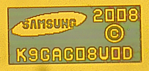
For the FLASH die, I was a bit surprised by how large it was. Before decapsulating the card, I was expecting to see one of two things: perhaps two die side by side, with the memory chip maybe about 6-7mm on a side and a 3mm/edge controller chip next to it, or a single fully-integrated FLASH + controller die. Instead, the memory chip is about 9 x 13mm — filling nearly the entire package edge to edge — and the controller chip is a sliver of silicon only 1.5mm wide and a shy more than 4mm long. Also, the actual FLASH chip die is simply a K9GAG08U0D, which is a common MLC device that you can also purchase in a TSOP package.
This is pretty clever on Samsung’s part. By sizing their commodity street FLASH to fit inside a microSD card, they are able to feather demand between popular SKUs. It’s also amusing that a full 32-bit ARM core is used as the controller between the FLASH device and the SD card interface. The world is just crawling with ARM controllers…
As for the winner, a bit tough to pick this time. A lot of people walked around the answer, thrown off by the CMP fill tiles, and assuming the device had something to do with a secure system.
The metal squares, while they do obscure the circuitry beneath them, are not active elements nor are they put there for the purpose of security. They are there actually to ensure that the fill density of metal versus dielectric is within a certain ratio. This is due to a requirement of a process known as CMP (chemical-mechanical polishing), where a chip’s active surface is planarized, layer by layer, by rubbing abrasive pads with a fine-grit chemical slurry across the surface. If the fill ratio is not obeyed, then portions outside the ratio will either polish too quickly or too slowly due to the differential in hardness between the metal and the oxide dielectric, and the result will be a non-planar surface.

You can see the fill density equalization going on in the picture above. The very large silvery tiles are from a very coarse top layer metal used just for bonding pads. The copper-hued tiles are from a lower wiring layer. You can see just a few of those wires in this photo. The area immediately around the wire has no tiling, but the otherwise open expanse is entirely filled in to ensure that the sparse, tiny wires don’t get polished away during the CMP operation.
Thus, when you see CMP tiling you know you are dealing with a deep submicron process with a lot of metal layers. Also, active protection meshes typically do not use unconnected pieces of metal; instead, the metal is connected in a series chain so damage to any individual element is easily detected by the monitoring circuit.
Since MegabytePhreak is the first answer to use the term “microSD” explicitly, he/she is the winner (by just 3 hours over Burlap). Congrats! email me for your prize.
[…] microSD ware for January 2010 was not an incidental post. It is actually snapshot of a much longer forensic investigation to find […]
Hey man
Nice post.
Another awesome blog Yahoo showed me. Subscribed to your RSS
I will be visiting this site again
can you or anyone advise me on how it may be possible to get the physical data bits-by-bits off microSD ? Or kindly advise me on where I can find the information I need. I can’t seem to even find info on microSD ports on the internet.
Bunnie,
Once again you amaze me by proving that regardless of topic, you find a way to make it interesting as hell!
Your mind, and the way it works should be an international treasure. Please continue, and of course, thanks for sharing!
db
These are the best ways to generate content for your blog. It is advisable not to go with the automated path. If you do select to do that, you will probably have lots of content- but the substance of the text is unlikely to increase traffic for you. Putting in some lovely, old-fashioned content work will yield better results for you. As the expression goes- “you get out what you put in.
i host 5 of my blogs on Blogspot and it is really good for beginners. but if you want something with more features, nothing beats wordpress~.~
Very good article! This is a extremely beneficial web-site that you have.
As a bit of a tech junkie, I am utterly impressed whenever I see the advances in micro technology. A billion transistors in that one section of die is insane. Makes me want to crack open the microSD cards I have laying around.