The Ware for December 2015 is shown below.

This ware got me at “6502”. Thanks to DavidG Cape Town for contributing this specimen!
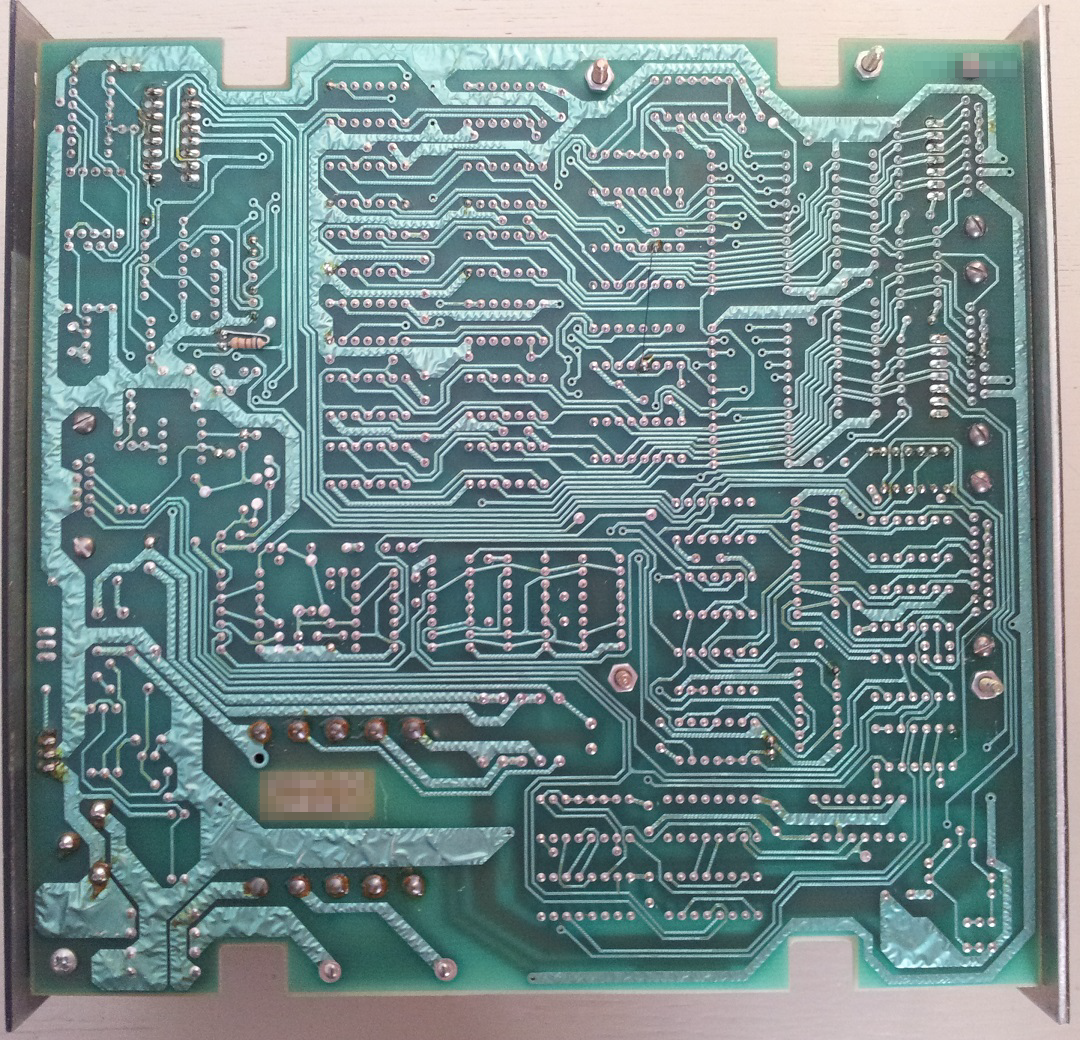
One question for the readers (separate from naming the ware!), it’s been something I’ve wondered about for decades. On the back side of this board, one can see ripples on the fatter traces. My original assumption is this is due to a problem with hot air leveling after the application of a solder finish to the bare copper board, before the soldermask is applied. However, the top side is almost entirely smooth, so clearly the process can supply a flatter finish.
So here’s my quandary: are the ripples intentional (for example, an attempt to increase current capacity by selectively thickening fat traces with a solder coating), or accidental (perhaps microscopic flaws in the soldermask allowing molten metal to seep under the soldermask during wave soldering)?
Been wondering about this since I was like 15 years old, but never got around to asking anyone…
Happy holidays to everyone! I’ll be at 32C3 (thankfully I have a ticket), haunting the fail0verflow table. Come enjoy a beer with me, I’m not (officially) giving any talks so I can actually sit back and enjoy the congress this year.
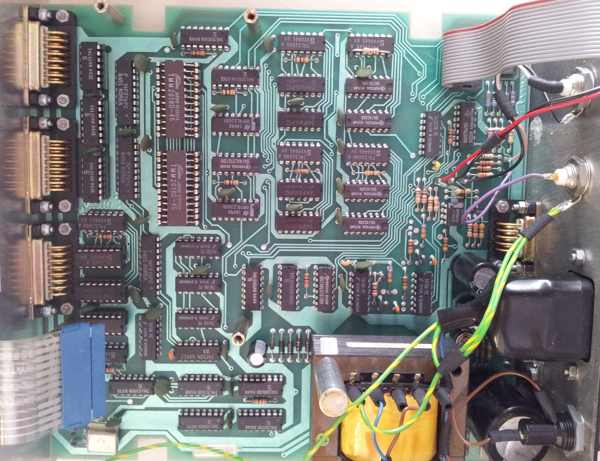
Some testing/measuring equipment? It has some trigger inputs/outputs, two indicators and a keyboard.
Whenever we use solder to fatten up the traces a bit on a specific part of the board, it’s normally done by leaving the solder mask exposed and relying on the pickup from wave soldering to do it. That wouldn’t result in it being under the solder mask, unless it was done by the board house. That’s not something I’ve ever seen offered, although not impossible.
Using a selective solder bath might do it, but wouldn’t it be difficult to do with enough selectivity to avoid needing to manually clear the through-holes for later assembly? If the solder was added manually by hand, I would expect something that looked more like a tig-weld.
I’ve seen traces ripple like that on boards that have been overheated and had the glue melt/outgas, but that wouldn’t explain how it was so uniform and selective to the large traces.
Could it be some kind of selective electroplate process for a couple of specific nets? That still wouldn’t explain the texturing.
The interesting thing about this device seemt to two of the 15pin connectors on the bottom PCB that stick out on the bottom front of the device. They seem to consist of 8 “data” input pins and a row of GND/Vcc. This is on the upper left of ntw_dec_2015_b.png.
Adjacent to the two upper 15pin connectors, you see 74LS14 buffers with schmitt-trigger inputs and ‘374 octal D-Type flipflops (“F”ast… :-) ) that directly interface to the TMM2018D-45 “fast” SRAMs DQ (data in/out) pins. The address pins are connected to the 74LS161 counter nearby (at least some of them) which would generate increasing addresses.
So, certainly this device takes 16 digital inputs from the frontpanel and stores them sequentiallyin the two 2kB RAMs.
The bottom and top PCBs are only connected by a 16pin ribbon, so there’s not enough pins to route more than 8bits + a few control signals to the 6502 on the upper board. Certainly, the RAMs aren’t accessed “directly” (as in: on the address/data bus). The CPU reads a membrane keypad (flex-cable into blue socket) and outputs to two multiplexed (I guess 7-segment or similar) LED displays.
So, one guess would be a very simple, old logic analyzer? Possibly with output to a serial terminal (the 9pin DSUB on the back?)
The “fast” opamp in the back the the two BNC connectors make me think if maybe an analog scope could be used to show the traces? Trigger with one BNC output, then output the samples of each trace sequentially, with a offset being increased after each trace?
(e.g. TRIG, output Ch0(0..0.5V), TRIG, output Ch1(0.6..1.1V), TRIG, output Ch2(1.2..1.8V)…)
Here’s a picture of a “hobbyists grade” logic analyzer from the 80s:
https://archive.org/stream/radio_electronics_1984-01/Radio_Electronics_January_1984#page/n44/mode/1up
Not the “Scope” and “Sync” BNCs on the frontpanel, so my speculation to display on an analog oscilloscope doesn’t seem to be that far off.
I second this.
Great findings. As far as the manufacturer goes, I would guess it is Kontron. I own one of their bench multimeters from the same era, and the style of the PCB and especially the wiring just shouts “Kontron” at me – the way the PE wire is connected to the enclosure, the little rubber tubes around the solder contacts at the fuse holder and transformer, … I fail to find a matching unit when searching for “Kontron Logic Analyzer”, however, so I have to leave this to someone else, I guess…
I always assumed the ripples formed during wave soldering… but were due to thermal expansion on the larger metal traces. Never had that confirmed either…
Dave Jones (EEVBlog) mentions that ripple effect regularly in his webcast. One of these explanations can be seen at https://youtu.be/0-IebArtT9I?t=5m14s (#557 5m14s in case the URL disappears) .
TL;DW, the ripples are an unintentional artifact of the tin plating process and occur before solder mask is applied to the board.
Great find, thanks for posting!
As far as I know the ripples are unintentional, but not caused by flaws in the solder mask: The board was simply tinned before the solder mask was applied and the tin melted during wave soldering. It’s a slightly different production process compared to the “modern” SMOBC (Soder Mask Over Bare Copper).
I wonder what the dirty IC in the bottom left of picture A is – it’s hidden by the ribbon cable in picture B. The resistors that are connected to its pins seem to be the only higher-precision resistors on the board, possibly the DAC that is needed for Christian’s theory.
I’m also surprised that the Varta battery hasn’t leaked yet. =)
…accidental (perhaps microscopic flaws in the soldermask allowing molten metal to seep under the soldermask during wave soldering)
That one. I’ve only seen it on the bottom of wave-soldered boards.
On a related note, does anybody know how/why green became the traditional color for PCB solder masks?
My thought is it’s one of the soldermask colors that’s easiest to inspect, that’s not simply transparent. You want some color so you can easily find holes in the soldermask — so you wouldn’t use clear. But you also want to see the traces, which is why for example black is bad.
My second thought would be there’s some property of green that’s good/cheap for the kinds of photopolymers that compose the soldermask, but probably soldermask was green even before they used photoprocessing to develop soldermasks.
Looks like some kind of captioning or otehr on-screen overlay, maybe time.
Or maybe even some kind of SMPTE encoder or decoder.
It does look like a logic analyzer or perhaps a 16-channel digital adapter for a scope. As mentioned, the top two DA15 look like 16 inputs, and the bottom one, with the ’86 xors may be a trigger match circuit.
Behind the crystal looks like a clock divider with selectable output (‘153 demux). The 9-pin connector is not serial (serial ports were 25 pin at the time of this device…)
With respect to the tinning before solder-mask: That makes a lot of sense. I thought that the difference between large and small traces was too large for it to be a ‘bulk’ process like that, but looking closer, it looks like all the traces exhibit it to a certain extent and that it’s just more visible on the larger ones.
Yea, I always figured the ripply solder was because of wave soldering.
Agree, keyboard, LED display. The two BNCs made me think “packet node controller” but I agree, the 16 inputs to the video RAM and then to the shift registers looks more like a logic analyzer.
How a PCB is made: photoresist is applied. Tin is electroplated where there is no photoresist.
Then, the photoresists is stripped, and the tin plating protects the copper during etching.
One can keep the tin plating. Applying a solder mask over it is possible, but it will wrinkle when soldering. Tin melts, solder creeps under it.
Nowadays, the tin is stripped off before the solder mask goes on. Problem solved.
Googling “Miracles in tin stripping” will lead to a site with a lot of information on the chemical steps.
Thanks. That just made a few other things I’ve seen happen in PCB shops make a lot more sense!
The plating could also be tin/lead alloy (i.e. solder). A tin/lead alloy would be much more likely to melt under solder mask in wave soldering causing the rippling. I know from internal documents that Digital Equipment used tin/lead alloy as the etch resist plating and the ripple effect was common on boards they made.
My analysis was that this looked like test equipment (due to the front panel LED displays, BNC connections, and general feel of the layout). It was obviously not analog as D-Subs are not generally used for analog measurements and there was a lack of analog front ends. Like the other posters here I tended towards a logic analyzer, although there was always the possibility that this was simply an interface for a larger system. I pulled the year off of the chip date codes and image searched for logic analyzer with various years in that era. The 1983 search lead me to the Thurlby Thandar Logic Analyser LA-160. The front panel with the three D-subs, two quad 7-segment LED displays, and the flexible button membrane match these internals perfectly. Unless someone else re-branded this instrument, I think this has to be it.
I do believe you have it. I found this page on the LA-160 and it has photos of a couple parts of the PCB that match perfectly. See the photos of the EEPROM and the area with the battery. The component placement and traces are identical.
http://sonicsheep.com/Electronics/3-LA160%20Writeup.htm
I think you’ve nailed it.
There’s a service manual for this logic-analyzer on this pretty strange website: http://elektrotanya.com/sinclair_thurlby_la160_logic_analyzer_sm.pdf/download.html (the download-link, initially labeled “…processing…” takes a minute or so to appear).
The board-layout diagrams on pages 16 and 17 exactly match the photos.
Congratulations, this must be it. So far, I have not seen any re-branded instruments by Thurlby, but it looks like RS components, the UK based (?) distributor, have co-branded some versions of it.
A photo of the RS rebranded version, exterior (you can even rent it as a movie prop): http://www.tvfilmprops.co.uk/det/1551/Thurlby-LA160/
Regarding the PCB. As what Thomas said except that for some boards they would then dip the tinned PCB in lead. You then had the option of having the board Hot Air leveled if you wanted a neater finish.
http://www.sunstone.com/pcb-capabilities/pcb-manufacturing-capabilities/surface-finish/hot-air-solder-leveling-%28hasl%29
hmm 2*8b*2k ram on 16 inputs and counters…..
8 (probably hex?) characters on LEDs
hmmm…..
Things it is not :
– it’s not an ICE (no real time from the processor)
– it’s not a frequency counter
– it’s probably not a logic analyzer (no real screen)
This thing stores real time signals on 16b with some triggers, and displays some chars. Eventually displays on PC via RS232 also…
it might be some kind of bus tracer for a 16b uP bus
The solder thing :
These boards have a solder coating under the mask ( typical from the time, probably HAL). When you pass that onto the wave, it reflows and forms this pattern, the solder mask gets soft and loosely retains it in liquid pockets
Here’s my experience with the rippled traces. About 21 years ago I started my first job out of college at a company that thought they could save money by manufacturing their own PCB assemblies. We bought the circuit boards from a PCB fabricator with HASL finish. When we got the boards the traces were flat. We stuffed the components and ran the board through the wave solder machine, and to my surprise they came out with this rippled effect. I was worried that the traces had delaminated from the fiberglass from too much heat, but when I tried to push the trace back down it was clearly solid and thick – not raised off the PCB. Somehow the solder had wicked under the solder mask and raised it without damaging the solder mask. All the traces, except maybe the narrowest, had this effect to some degree, but it was worst on the larger traces and ground plane areas. At some point I took an expendable board and cut down through the ripples and verified that it was indeed excess solder that had flowed between the trace and solder mask. The copper trace was still flat on the fiberglass. It didn’t hurt anything so we didn’t really worry about it.
But they quickly abandoned using that old wave solder machine. The pump was bad and occasionally the solder wave would “bounce.” If the leading edge of the board was arriving right at that time, you had the horror of watching a flood of solder go over the front edge of the board and flood around all the top side components you spent an hour or two stuffing by hand.
Later we switched to a different type of finish on the PCBs and didn’t see the ripples anymore.
Well, it looks like this may have been decided already, but I was wondering if it wasn’t an ESE remote master clock display, taking IRIG-B timecode over coax; you didn’t show the front and back panels, and I assumed that was on purpose…
I like the idea, IRIG is (I think) sufficiently obscure so that something in the vicinity would make a pretty nice ware.
A pure display would need much less logic, though, could easily be decoded in software by the 6502. Anything doing proper timing related work would have had a PLL with a TCXO, a much more elaborated power supply and more BNCs for timing capture and refclock generation.
There’s a video on the EEVBlog (http://www.eevblog.com/2012/07/21/eevblog-317-pcb-tinning-myth-busting/) that talks about the thickness of the traces and measures the current capacity.
The original PTH manufacturing flow uses solder as a kind of resist. On inner layers, you put resist where you want copper to be, then etch away the unwanted part, then dissolve off the resist. Simple.
For outer layers, you start with 1/2 ounce copper, and put (uv-polymerizing) resist where you want no copper! Then you electroplate the whole board. This adds another 1/2 ounce to the exposed copper areas, and more importantly puts 1/2 of copper on the via walls.
Then you do a negative trick with etching: you coat the board in solder, which sticks to the exposed copper but not the resist, then dissolve off the resist, then dunk in an acid that dissolves bare copper but not tin/lead.
The result is the original 1/2 ounce copper is dissolved away and you’re left with tinned copper traces.
At this point, the tinned copper is nice and smooth (HASL). You can put solder mask over top of the whole thing.
But then you populate and wave-solder it. On the bottom of the board (and only the bottom), the tinning melts and flows under the solder mask, resulting in the patterns you see. (Solder surface tension fighting solder mask tensile strength.)
The top of the board stays cooler and doesn’t reflow, producing the asymmetry you see.
These days, solder mask is usually applied over bare copper, so you don’t get this effect.
Just to clarify: the solder isn’t getting under the mask during wave solder; it was already there. The ripples are of course more obvious on wider traces because there’s more slack under the solder mask.
I have seen those ripples on many boards from the 80s, I specifically remember the bottom sides of commodore PCBs an others of course. My VC-20 was especially bad in that manner (only that, of course, it had 5kb of ram, who could complain about that). These are not to increase current flow as the metal isnt any thicker there, its just lost its glue to the board for some reason. This means the original metal part didnt stay on the board epoxy base because the solder mask was liquified in the wave soldering process.
[…] Read more. […]