The Ware for June 2019 is shown below.
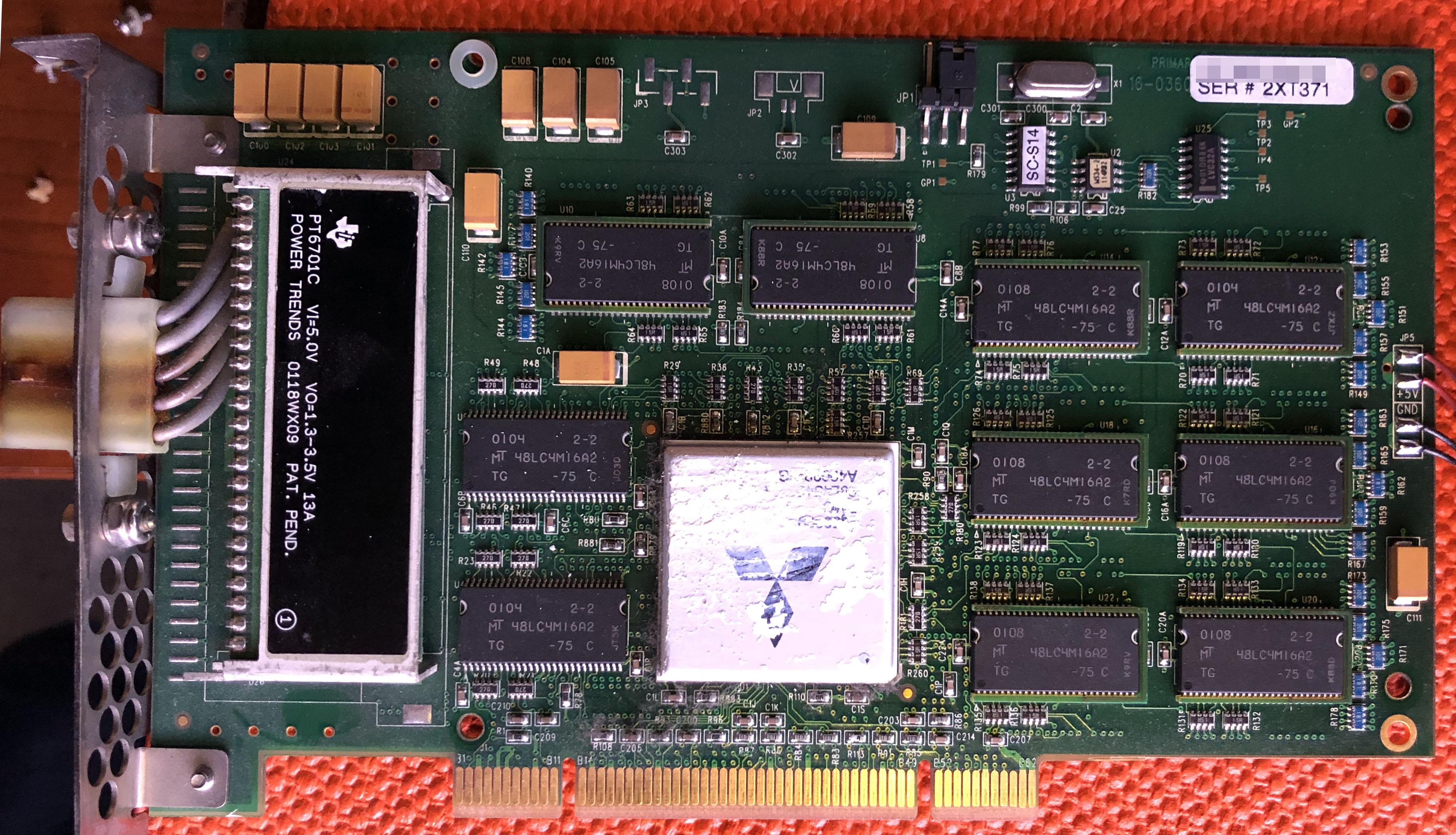
I found this particular detail to be entertaining:
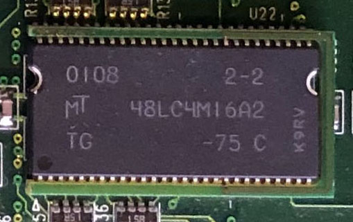
Some of the RAM chips have this tiny, thin PCB wrapping around three sides. That must have been a fun assembly process to develop and debug.
Thanks again to Patricio Worthalter for contributing this ware!
I think it’s an interface card (PCI Bus) used for calibrating and debugging the computer module(s) in cars. More specifically, from the logo on the one chip, I’d say Mitsubishi cars.
The date looks like 2001; by then just about all cars were OBD2. That connector looks like it took more current than a car computer deals with, too.
You’re right. and if I’d looked up the datasheet for the big black box on the left, I’d have seen that it’s a programmable power supply, capable of outputting 1.3-3.5V @ 13A.
And now that I think about it, the connector does look more like it’s meant for power than for data.
Definitely NOT a programming interface.
Is this a card to drive some form of mechanical actuator such as oscillating tables? The RAM chips would hold the arbitrary waveforms and the black module on the left would be the power driver of the motor or voice coils or something like that.
Was going to suggest just that; it seems unlikely that many memory modules would be needed for a simple configurable power supply. Tables for a pattern generator or similar is more plausible.
I see no reason to conclude it has anything to do with Mitsubishi automobiles because they had at least one microprocessor line (https://en.m.wikipedia.org/wiki/Mitsubishi_740) which would make sense in this era and context.
I thought the little mini-pcbs were some weird (sort of socket (until I got to the second photo/description). Are they some sort of extended ground plane for noise mitigation? Odd that the couple of the modules on the left don’t have the same…
I think it’s some CC-Link card for communication with some industrial equipment. https://en.wikipedia.org/wiki/CC-Link_Industrial_Networks
Maybe an early cc-link controller?
I think you’re on to something. I was wondering why one of my links googling for “mitsubishi” + “pci” + “power” was already followed and then I realised I’d clicked your link earlier.
I think it’s some sort of coprocessor card requiring external power. The back connector feeds power to the board which is regulated by the programmable supply to power the Mitsubishi chip (and RAM). This talks to the host via the PCI interface.
I think this is the controller for a video wall or the like. LEDs, maybe?
The hardware would fit this, and Mitsubishi did make those things in the past.
Looks like a “Mitsubishi PCI Volume Renderer Real Time Visualization Volume Pro 500 40-0360”, some 3D coprocessor card, without the cover
https://www.ebay.com/itm/Mitsubishi-PCI-Volume-Renderer-Real-Time-Visualization-Volume-Pro-500-40-0360/151653790143?hash=item234f4531bf:g:KKQAAOSwPhdVH-06
Here’s an interesting whitepaper on it, it was intended for real-time rendering of CT scan data: https://vcglab.org/gvi-files/SIG99_0.pdf
Bravo. You nailed it. And thanks for the white paper also @jackw01
Seems like I messed up the link: https://www.ebay.com/itm/Mitsubishi-PCI-Volume-Renderer-Real-Time-Visualization-Volume-Pro-500-40-0360/151653790143?hash=item234f4531bf:g:KKQAAOSwPhdVH-06
Wow, cool stuff. This chip is called the “vg500”, and there is a siggraph paper
about it.
Those eight memory chips with the tiny pcblets are the “voxel memory”. One theory
I have is that this PCB changes the pinout so this dram chip can be used in place
of the one this board was designed for, but the pixel memory and section memory
(the other two chips) doesn’t have an adapter board, so that doesn’t sound very
likely.
(There are twice as many drams actually, the other half is on the other side of the
board).
Oh and this is PCI VID:DID 10ba:1002 :-)
https://www.merl.com/publications/docs/TR99-19.pdf
There’s also a hotchips paper:
https://www.hotchips.org/wp-content/uploads/hc_archives/hc11/3_Tue/hc99.s5.4.Pfister.pdf
Fascinating stuff :-) Amazing to see what was possible at 350nm already, too.
Looks like Jean aced it.
Wow, cool stuff. This chip is called the “vg500”, and there is a siggraph paper
about it:
https://www.merl.com/publications/docs/TR99-19.pdf
There’s also a hotchips paper / presentation:
https://www.hotchips.org/wp-content/uploads/hc_archives/hc11/3_Tue/hc99.s5.4.Pfister.pdf
Those eight memory chips with the tiny pcblets are the “voxel memory”. One theory
I have is that this PCB changes the pinout so this dram chip can be used in place
of the one this board was designed for, but the pixel memory and section memory
(the other two chips) doesn’t have an adapter board, and use the same chips, so
that doesn’t sound very likely.
(There are twice as many drams actually, the other half is on the other side of the
board).
Oh and this is PCI VID:DID 10ba:1002 :-)
Fascinating stuff :-) Amazing to see what was possible at 350nm already, too.
Good job guys.
dobre okna
I believe the PCB that wraps around the DRAMs are used to stack a second DRAM on top of the first one. I have seen some SGI systems from this era do the same.