The Ware from December 2023 is a 20-watt laser diode used for engraving. It’s used in products like the ATOMSTACK Laser Engraver (link without affiliate code), and the module itself is produced by Shenzhen Xinghan Laser Technology Co, Ltd.. I don’t have an exact part number for it, but it is a blue-wavelength (so presumably 450nm), quad-laser diode module with a net power output of around 20 watts. I recently saw a LaserPecker (sans affiliate) in action and it’s impressive how solid state lasers have transformed engraving/cutting technology — my first laser cutter from 20 years ago was the size of a desk, cost over 10x as much, and was a lot harder to use.
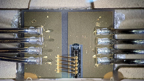
As for a winner, it’s pretty tough to pick one since a I found several comments quite insightful. The main thing I personally wanted to figure out was the structure of the picture above: why was there a smaller device stacked on top of a larger device? I originally thought the gray-ish lower substrate was the laser, and the small part on top was a protection diode; but after reading the comments I’m now of the opinion that it’s probably a CVD diamond heat spreader, and the laser is the very small black-ish bar on top.
I found another image I had in my collection of the device lasing, and indeed the small bar was the part that was emitting light. It’s also the case that the lasers are at stepped heights. If memory serves correctly, the beam shape of these laser diodes tends to be rectangular, so by “stacking” the beams next to each other you can get a more square profile to the net output pattern. I was also surprised not to find any sort of optical feedback mechanism for power monitoring, or obvious protection diodes — but maybe the control circuitry and fabrication process is just so dialed in now that it’s not necessary? Or perhaps something else very clever is going on that’s not discernible in these photographs.
It’s a tough call, but I’ll give the prize to FETguy — for convincing me that the lower chips are probably CVD diamond, and noticing the stair-step structure. Congrats, email me for your prize!
As a brief postscript, looking at all the progress in high power laser diodes made me wonder if cheap HDI PCBs are around the corner (I have a blog post that goes more in-depth into HDI PCB construction, in case you’re interested). The biggest capital cost barrier has traditionally been the huge laser CNC machines needed to cut the vias, compounded with the fact that these expensive CNC machines can only drill a single board at once (as opposed to the mechanical drills that can penetrate a stack of ten or more PCBs in a single drill hit).
Unfortunately, it looks like we’re still an order of magnitude away in terms of the peak power and beam profile necessary to drill a good, clean hole in an HDI substrate, but it also looks like there’s plenty of manufacturers with their eye on this niche. A cursory review of the literature also seems to indicate that whatever is being used to drill the holes probably has to retain at least one mechanical axis (with perhaps a single galvo plus a parabolic reflector) because a two-galvanometer solution will have problems with the laser spot impinging at an angle toward the edges, which is undesirable for a PCB via.