The Ware for December 2023 is shown below.
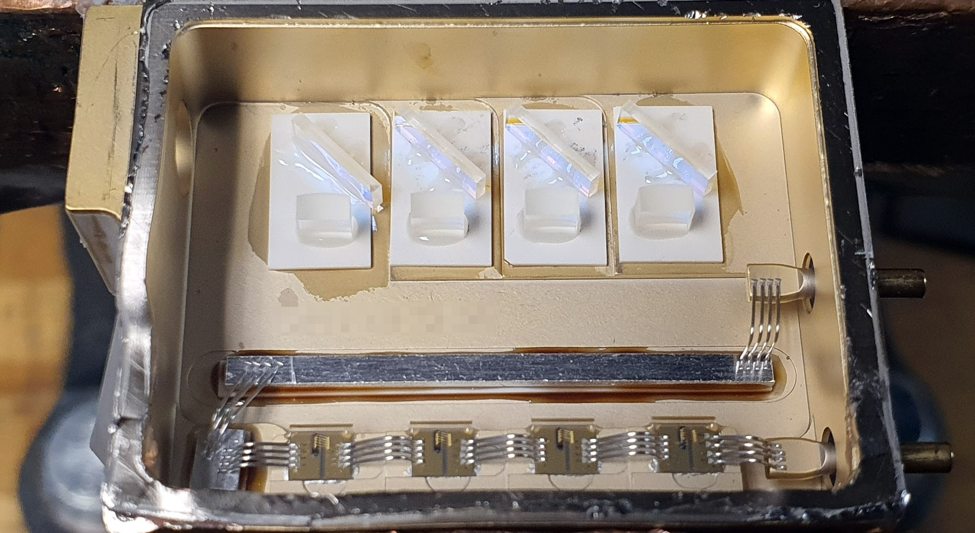
Thanks to Cedric Honnet for contributing this ware! Unfortunately this image does have an exact hit on Google images, as it is already in Cedric’s social media feed — but I think the ware itself is functionally interesting, yet simple enough to guess without having to rely on image searches.
Thus answers will be judged in part based on their insight into the reasoning behind the construction of this ware — for example, what’s going on in the zoomed in view of the ware? What are some of the considerations in building a module of this nature?
Happy new year! Name that ware will be wrapping up its 18th year soon
Fairly obviously a diode laser module, with 4 dies feeding the 4 collimator/mirror assemblies and firing out the top left of the zoomed out image. In the zoomed in photo it looks like the black rectangle is the semiconductor, mounted on a presumably ceramic substrate (to electrically insulate from the housing and conduct away heat). As for why they use that elaborate bus-bar… I guess to keep the wirebond assembly easier? Perhaps they test each laser die separately and align the optics before bonding the main connections?
One observation: The laser mounts and their optical parts step up from left to right in height above the bottom of the enclosure. Not sure why.
I think the gray insulating wafers under the individual lasers are CVD diamond for its thermal conductivity. Maybe part of the reason the aluminum bond wires are kept away from the lasers is to heat sink them, too. Of course, the bond wires to the lasers are gold.
So if the optical parts step up from left to right does that mean that each laser shoots over the top of the optical parts for the lasers to the left?
Curiosity got the best of me so I read the blog post, so I know that for this thing’s purpose, the 4 lasers all have to converge on one point somewhere outside the enclosure.
Therefore, it seems like alignment would be critical, but there are no adjustments for alignment. Does someone in a factory have to place each optical element, align it with the lasers on, then glue it in position?
Could they align it in reverse? ie shine in a low power non-pulsed laser and align the 4 dots on the fronts of the 4 lasers? Or would that be too rough?
I like the idea regarding reverse alignment but I think two challenges come to mind; the collimator is now expanding the reversed beam so aligning the laser diodes will be harder (no longer aligning a smaller, focused beam), and the actual diodes themselves need to then be aligned in regards to 5-degrees of freedom (x, y, z, pitch, and yaw — they also may need roll to keep polarization angle the same but guessing that’s automatic based on their package+wiring), so it’s likely easier to place the lasers first, and then adjust everything else based on their outputs since the optics are much larger so more tolerance for where they’re placed relative to the diodes.
I am curious how they really do it though and order of operations! Recently built a similar setup of 3 [diff wavelength, TO-38 can] laser diodes, collimators, and dichroic mirrors for beam combination and it wasn’t fun!
Good eye on the steps @FETguy, I didn’t notice them until reading your post! I was initially confused by the setup but the steps resolve the confusion.
@Carl Smith, you’re exactly right – the steps are for each laser to shoot over the next mirror. The diodes are going to be the same wavelength in this application (if they weren’t, then different dichroic mirrors could be used to reflect some wavelengths while transmitting others). Let’s assume the mirrors (which look dichroic) allow 90% of the light to reflect, then 90% of right-most laser will reflect of right-most mirror but then hit 2nd-to-right-most mirror and reflect again, unfortunately going towards the case, so only 10% of that light would make it out, and a continued pattern moving leftwards. Regardless of % there would be large losses where the steps allow nearly all the light to escape.
Another potential design to help focus more light in a spot could be to remove the right half of the design, then mirror the setup with X axis as mirror line, rotate the diodes on one side 90˚ to rotate their polarization, then combine the two separate beams with a calcite prism so the output would be a hash (#) with most energy focused in the center rather than a 4-step (||||) rectangle. This might even further increase the energy as there’s less chance for destructive interference from all lasers having the same polarization as aligning all 4 to not interfere at all is going to be challenging with no easy adjustments at short wavelengths (~455nm).
Is it a transceiver for [C|D]WDM? The mirrors and prisms would split/combine light into colors so you can run multiple channels on the same fibre. (I didn’t search the image yet, that seems like cheating.)
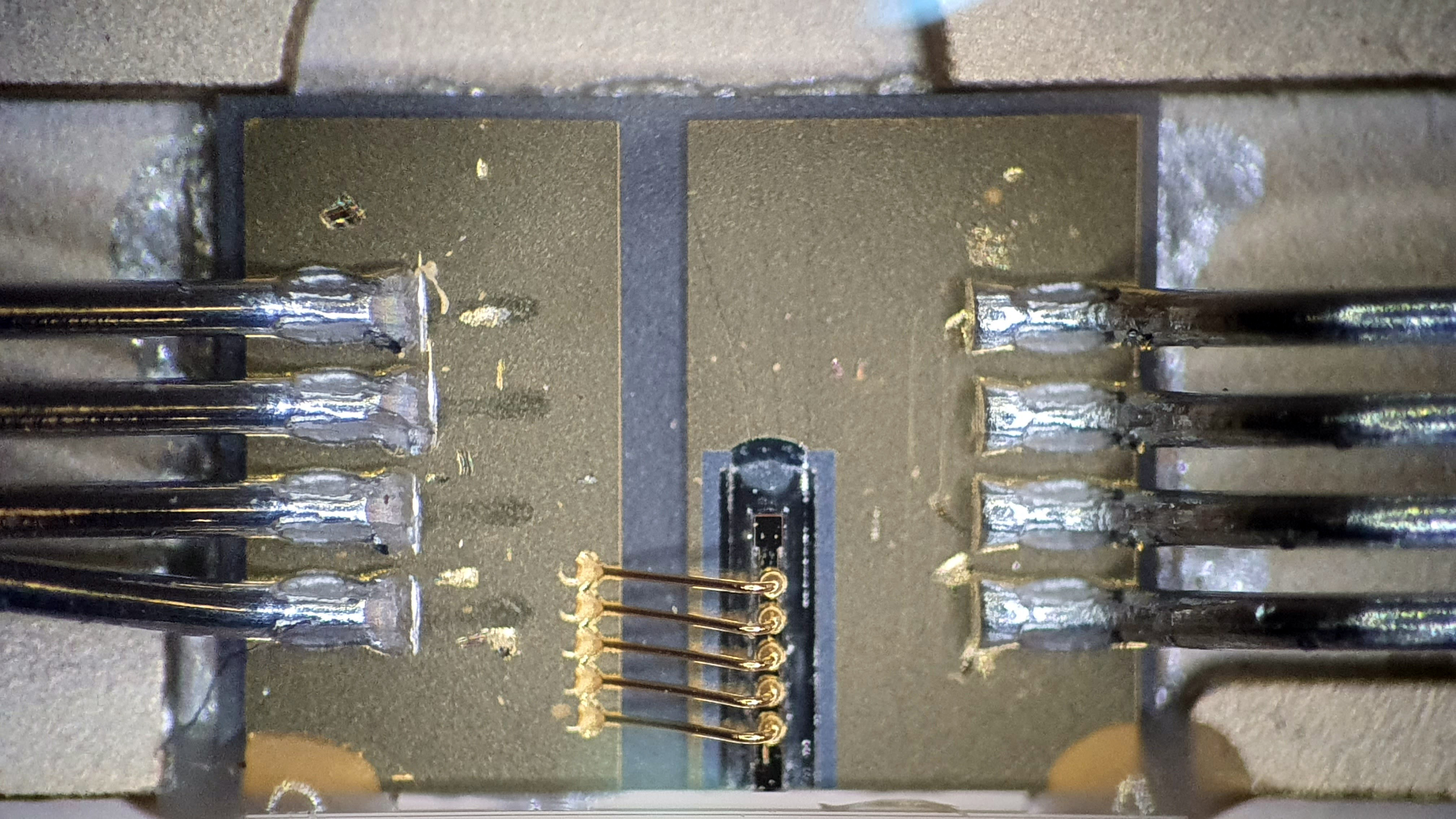
If I assume the long, thin element is the laser (terminal on top + case as return) then the stack of items along the bottom must be intentionally failing diodes.
I suspect the function of the diodes is to block all current until a threshold voltage is met, then suddenly short/avalanche/break-down. If you power this assembly with a HV capacitor and slowly charge it up then the diodes will auto-trigger at the right voltage and allow a larger current pulse through the diode. Feed a constant current into the capacitor and you will have an auto-repeating laser pulse.
The diode construction is gorgeous. It’s macro — they stacked pieces together with tweezers and glue. I suspect they made whole wafers of the same (special breakdown) materials and then chopped them up into these pieces. Perhaps the substrate itself had a mask (two golden squares) but they are so big you could have almost used sticky-tape.
The large surface area means they must be able to survive very high current pulses but probably also leak badly. Leakage is unlikely to be concern in this application as the laser won’t hit lasing threshold with small leakage-level (mA?) currents & voltages.
There are no sensors in this box, it’s purely a source. My original guess for its purpose was a low power sensing apparatus like a spinning 4-spot lidar, because I assumed only a smart amount of light would get coupled through those optics and out. After looking at the source Twitter post I discovered I am _very_ wrong :D
On second thought: I’m probably way off.
The 4 diodes on the bottom contain long, thin elements that are perfectly aligned with the optics on the other side. These are probably end-firing diode lasers.
The back of the case (bottom of photo) probably acts as a mirror on one side of the laser OR it’s internally mirrored (inside the wafer edge).
The long, thin element in the middle is a partial reflector, possibly electrically gatable or maybe they’re just using it as a convenient grounding strip.
Judging from the color of the mirror’s coatings I think all four laser diodes are the same wavelength, i.e. this is a monochromatic setup. But there is no temperature stabilization nor any external cavity feedback via a grating or similar and thus the four laser diodes have different modes and run freely in terms of light frequency.
Furthermore, I do not think that the laser beams are perfectly overlapped, because the optical setup of each laser is on a different height. If you look closely, the laser diodes and optics are placed on four different heights of a step-like structure, maybe less than a tenth of a millimeter apart. This is only a small difference compared to the expected beam diameter of a millimeter or so.
The cube-like optical elements are cylindrical lenses to shape a round beam out of the elliptic beam exiting the laser diodes.
The wirebonding is also nice to look at. Especially if you think about the manufacturing procedure. All thick wirebonds to the laser diodes are made from right to left, except the one on the furthest left, which is from left to right. The reason for the additional small conductor disk on the left might be to have easier access for bonding, but also to reduce any force on the diode laser substrates. The wirebonds act as springs and with this configuration each substrate has two sets of wirebonds pulling in opposite directions and thus the overall force is zero. This is important to not missalign the optical setup during glue curing.