The Ware for May 2025 is shown below.
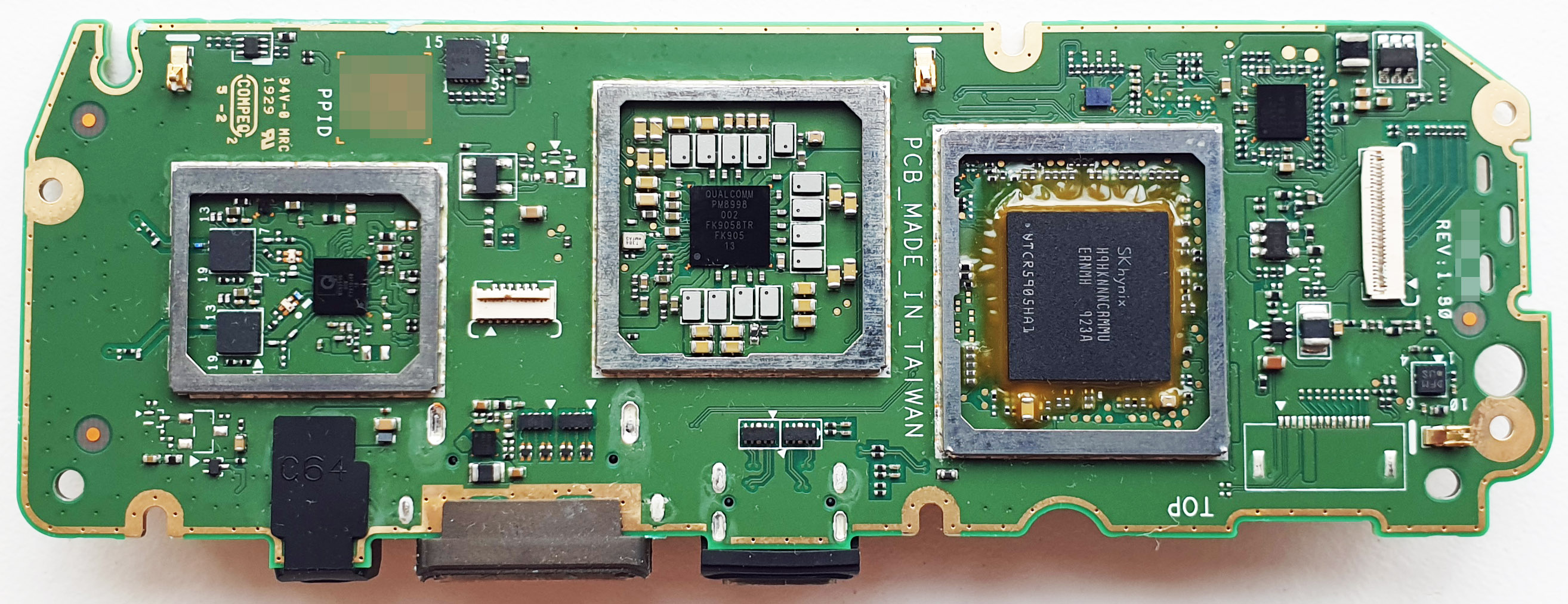
Because I really like to be able to read the part numbers on all the parts, here’s a couple more detail images of portions that didn’t photograph clearly in the above images.
This ware was donated to me by someone in person, but unfortunately the post-it note I had put on it to remind me who it was had long fallen off. My apologies; if you happen to see this, feel free to pop a note in the comments so you can be attributed for the contribution.
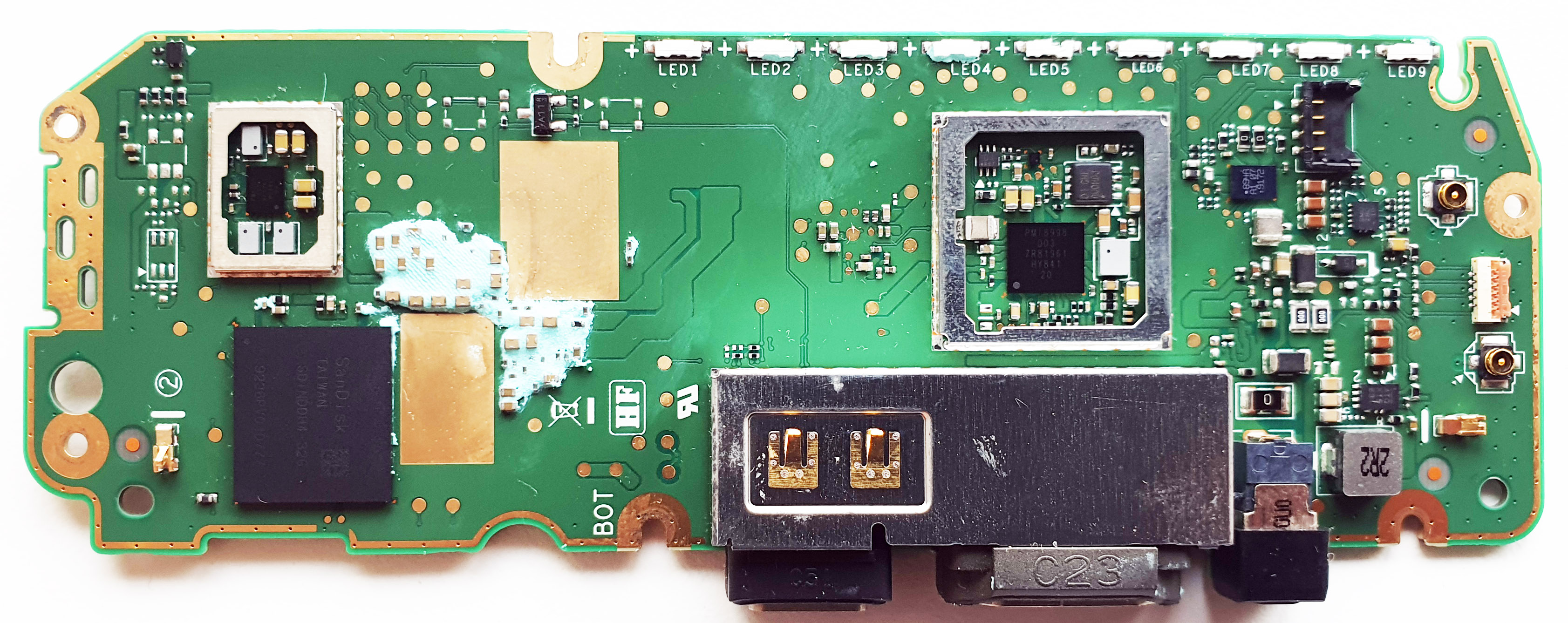
I made a point of not looking up the details of the ware before I did the teardown, so I could have a little fun figuring it out. While pulling it apart, the entire time I kept muttering to myself how this ware reeks of silicon valley startup with more money than sense. The hardware engineers who worked on this were clearly professional, well-trained, and clever; but also, whoever the product manager was had some Opinions about design, and incorporated lots of cost-intensive high-tech “flexes”, most of which I’m pretty sure went unappreciated and/or unnoticed by anyone other than someone like me taking the thing apart. For example, the board shown above is encased in a thixomolded two-part magnesium thermal frame with heat pipes, precision-machined thermal conduction blocks and gobs and gobs of thermal paste, which then necessitated a fairly tricky assembly procedure, and some brand-name custom-designed antennae to work around the Faraday cage caused by the metal casing. You’ll also note that despite the whole assembly being stuck in a metal case, each circuit subsystem still had an RF cage over it – so it’s metal cages inside a metal cage. This project must have had one heck of a tooling budget.
This was all for the sake of a “clean” design that lacked any visible screws. I’d say it also lacked visible cooling vents but ironically the final design had prominent ribbed structures, but they weren’t used for cooling – they were purely cosmetic and sealed over with an inner bezel. I feel like most of the cost for the thermal frame could have been avoided if they just let some air flow through the product, but someone, somewhere, in the decision chain had a very strong opinion about the need for a minimalist design that left little room for compromise. I would lay good money that the argument “but Apple does it this way” was used more than once to drive a design decision and/or shame an engineer into retracting a compromise proposal. Anyways, I found this product to be an entertaining case study in over-engineering.
It appears to be a facebook portal TV which explains the money thrown into it.
The audio DSP led directly to the iFixit teardown which feels like cheating as far as these things go.
That’s fair enough. I thought the audio DSP was an interesting detail because they already had an enormous CPU/GPU complex in the system. Like…why…
That does seem like cheating. iFixit identifies one chip on there as a “GMA253” 3-axis accelerometer, maybe actually the BMA253, it is the right package and has the letter “U” where the data sheet says in the marking. But why does a product like this need that? Isn’t this thing meant to just sit on a shelf or something? It doesn’t look like you’d pick it up and twirl it around.
It does looks like some sort of handheld game console looking board shape. Like a GBA or PSP.
Perhaps they’re using it to flip the camera image if this thing is mounted upside-down? The stand seems a bit odd for this, but I suppose it could be placed above or below a TV in either orientation.
Despite having been solved, I’ll play anyway: it’s a device based on a upper mid-range / top range Qualcomm mobile/compute platform from 2017/2018.
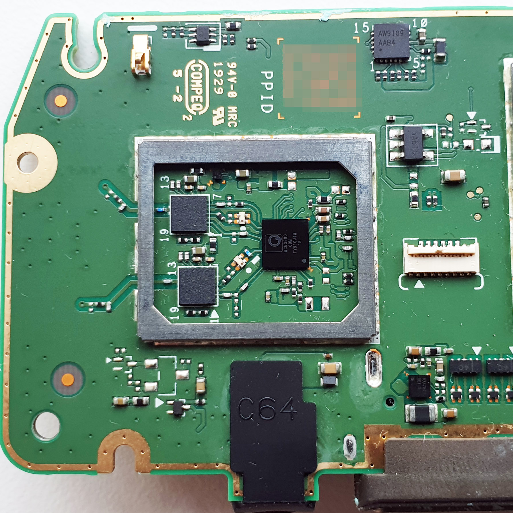
The SK Hynix 4GB LPDDR4X PoP ram hides the SoC, but both the WiFi module (WCN3990, 2×2 802.11ac, U.HF connectors for external antennas on the bottom side) and PMIC (PMI8990 + PM8990) are Qualcomm’s: this hints to a Qualcomm SoC, and given the fast ram I’d point to a powerful one such as the Snapdragon 835, which was available both as a mobile CPU and as a compute module.
Despite being built on a mobile platform, the cellular modem isn’t used: there is no SIM card slot and, while the SoC could support eSIMs, there are no antennas. Main focus is on WiFi.
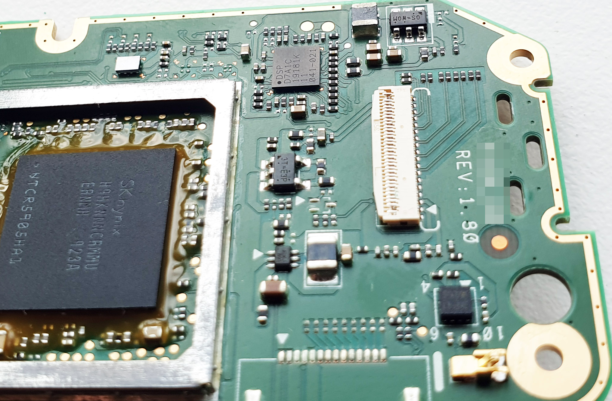
There is an external DSP (DSP D7A1C) w/ no datasheet available. Given the SoC already contains a DSP for camera and audio input, chances are it’s not powerful/featureful enough for the job and the external one is needed (e.g. multiple cameras for 3D/360° video, multiple/360° mic array).
The Sandisk flash is a 32GB UFS 2.1 module, both fast and small: it’s enough to hold the OS and minimal data. There is no microSD slot nor other storage: the devices doesn’t hold much data, and likely processes its A/V inputs in real time.
The board is small and of alongated shape.
On the bottom edge there are three connectors encased in protective rubber, for water and dust resistance; on the other hand the board doesn’t appear to be tropicalized / conformal coated: the case is supposed to be protective enough.
C64 could be either a 3.5mm jack or a barrel connector, C5 an USB Type-C connector, C23 maybe an A/V connector (HDMI or DisplayPort).
On the top edge there are 9 leds, which are both too many to be dedicated status indicators (it’s not networking equipment) and too close to be ambient light: my guess is a floodlight/flash for a frontal camera.
Cannot tell if the device is battery powered or not.
My guess is an augmented reality camera, such as Microsoft Kinect, with internal processing and output either streaming via WiFi or through the A/V connector.