Archive for the ‘NeTV’ Category

Developing Apps for Your TV the Easy and Open Way

Wednesday, June 6th, 2018

The biggest screen in your house would seem a logical place to integrate cloud apps, but TVs are walled gardens. While it’s easy enough to hook up a laptop or PC and pop open a browser, there’s no simple, open framework for integrating all that wonderful data over
the TV’s other inputs.

Until now. Out of the box, NeTV2’s “NeTV Classic Mode” makes short work of overlaying graphics on top of any video feed. And thanks to the Raspberry Pi bundled in the Quickstart version, NeTV2 app developers get to choose from a diverse and well-supported ecosystem of app frameworks to install over the base Raspbian image shipped with every device.

For example, Alasdair Allan’s article on using the Raspberry Pi with Magic Mirror and Google AIY contains everything you need to get started on turning your TV into a voice-activated personal assistant. I gave it a whirl, and in just one evening I was able to concoct the demo featured in the video below.


Magic Mirror is a great match for NeTV2, because all the widgets are formatted to run on a black background. Once loaded, I just had to set the NeTV2’s chroma key color to black and the compositing works perfectly. Also, Google AIY’s Voicekit framework “just worked” out of the box. The only fussy bit was configuring it to work with my USB microphone, but thankfully there’s a nice Hackaday article detailing exactly how to do that.

Personally, I find listening to long-form replies from digital assistants like Alexa or Google Home a bit time consuming. As you can see from this demo, NeTV2 lets you build a digital assistant that pops up data and notifications over the biggest screen in your house using rich visual formats. And the best part is, when you want privacy, you can just unplug the microphone.

If you can develop an app that runs on a Raspberry Pi, you already know everything you need to integrate apps into any TV. Thanks to NeTV2, there’s never been an easier or more open way to make the biggest screen in your house the smartest screen.

The NeTV2 is crowdfunding now at CrowdSupply.com, and we’re just shy of our first stretch goal: a free Tomu bundled with every board. Normally priced at $30, Tomu is a tiny open-source computer that fits in a USB Type-A port, and it’s the easiest way to add an extra pair of status LEDs to an NeTV2. Help unlock this deal by backing now and spreading the word!

Innovation Should Be Legal. That’s Why I’m Launching NeTV2.

Saturday, May 12th, 2018

I’d like to share a project I’m working on that could have an impact on your future freedoms in the digital age. It’s an open video development board I call NeTV2.

The Motivation

It’s related to a lawsuit I’ve filed with the help of the EFF against the US government to reform Section 1201 of the DMCA. Currently, Section 1201 imbues media cartels with nearly unchecked power to prevent us from innovating and expressing ourselves, thus restricting our right to free speech.

Have you ever noticed how smart TVs seem pretty dumb compared to our phones? It’s because Section 1201 enables a small cartel of stakeholders to pick and choose who gets to process video. So, for example, anyone is allowed to write a translation app for their smartphone that does real-time video translation of text. However, it’s potentially unlawful to build a box, even in the privacy of my own home, that implements the same thing over the HDCP-encrypted video feeds that go from my set top box to my TV screen.

This is due to a quirk of the DMCA that makes it unlawful for most citizens to bypass encryption – even for lawful free-speech activities, such as self-expression and innovation. Significantly, since the founding of the United States, it’s been unlawful to make copies of copyrighted work, and I believe the already stiff penalties for violating copyright law offer sufficient protection from piracy and theft.

However, in 1998 a group of lobbyists managed to convince Congress that the digital millennium presented an existential threat to copyright holders, and thus stiffer penalties were needed for the mere act of bypassing encryption, no matter the reason. These penalties are in addition to the existing penalties written into copyright law. By passing this law, Congress effectively turned bypassing encryption into a form of pre-crime, empowering copyright holders to be the sole judge, jury and executioner of what your intentions might have been. Thus, even if you were to bypass encryption solely for lawful purposes, such as processing video to translate text, the copyright holder nonetheless has the power to prosecute you for the “pre-crimes” that could follow from bypassing their encryption scheme. In this way, Section 1201 of the DMCA effectively gives corporations the power to license when and how you express yourself where encryption is involved.

I believe unchecked power to license freedom of expression should not be trusted to corporate interests. Encryption is important for privacy and security, and is winding its way into every corner of our life. It’s fundamentally a good thing, but we need to make sure that corporations can’t abuse Section 1201 to also control every corner of our life. In our digital age, the very canvas upon which we paint our thoughts can be access-controlled with cryptography, and we need the absolute right to paint our thoughts freely and share them broadly if we are to continue to live in a free and just society. Significantly, this does not diminish the power of copyrights one bit – this lawsuit simply aims to limit the expansive “pre-crime” powers granted to license holders, that is all.

Of course, even though the lawsuit is in progress, corporations still have the right to go after developers like you and me for the notional pre-crimes associated with bypassing encryption. However, one significant objection lodged by opponents of our lawsuit is that “no other users have specified how they are adversely affected by HDCP in their ability to make specific noninfringing use of protected content … [bunnie] has failed to demonstrate … how “users ‘are, or are likely to be,’ adversely affected by the prohibition on circumventing HDCP.” This is, of course, a Catch-22, because how can you build a user base to demonstrate the need for freedoms when the mere act of trying to build that user base could be a crime in itself? No investor would touch a product that could be potentially unlawful.

Thankfully, it’s 2018 and we have crowd funding, so I’m launching a crowd funding campaign for the NeTV2, in the hopes of rallying like-minded developers, dreamers, users, and enthusiasts to help build the case that a small but important group of people can and would do more, if only we had the right to do so. As limited by the prevailing law, the NeTV2 can only process unencrypted video and perform encryption-only operations like video overlays through a trick I call “NeTV mode”. However, it’s my hope this is a sufficient platform to stir the imagination of developers and users, so that together we can paint a vibrant picture of what a future looks like should we have the right to express our ideas using otherwise controlled paints on otherwise denied canvases.


Some of the things you might be able to do with the NeTV2, if you only had the right to do it…

The Hardware

The heart of the NeTV2 is an FPGA-based video development board in a PCIe 2.0 x4 card form factor. The board supports up to two video inputs and two video outputs at 1080p60, coupled to a Xilinx XC7A35T FPGA, along with 512 MiB of DDR3 memory humming along at a peak bandwidth of 25.6 Gbps. It also features some nice touches for debugging including a JTAG/UART header made to plug directly into a Raspberry Pi, and a 10/100 Ethernet port wired directly to the FPGA for Etherbone support. For intrepid hackers, the reserved/JTAG pins on the PCI-express header are all wired to the FPGA, and microSD and USB headers are provisioned but not specifically supported in any mode. And of course, the entire PCB design is open source under the CERN OHL license.


The NeTV2 board as mounted on a Raspberry Pi

The design targets two major use scenarios which I refer to as “NeTV classic” mode (video overlays with encryption) and “Libre” mode (deep video processing, but limited to unencrypted feeds due to Section 1201).

In NeTV classic mode, the board is paired with a Raspberry Pi, which serves as the source for chroma key overlay video, typically rendered by a browser running in full-screen mode. The Raspberry Pi’s unencrypted HDMI video output is fed into the NeTV2 and sampled into a frame buffer, which is “genlocked” (e.g. timing synchronized) to a video feed that’s just passing through the FPGA via another pair of HDMI input/outputs. The NeTV2 has special circuits to help observe and synchronize with cryptographic state, should one exist on the pass-through video link. This allows the NeTV2 to encrypt the Raspberry Pi’s overlay feed so that the Pi’s pixels can be used for a simple “hard overlay” effect. NeTV classic mode thus enables applications such as subtitles and pop-up notifications by throwing away regions of source video and replacing it entirely with overlay pixels. However, a lack of access to unencrypted pixels disallows even basic video effects such as alpha blending or frame scaling.

In Libre mode, the board is meant to be plugged into a desktop PC via PCI-express. Libre mode only works with unencrypted video feeds, as the concept here is full video frames are sampled and buffered up inside NeTV2 so that it can be forwarded on to the host PC for further processing. Here, the full power of a GPU or x86 CPU can be applied to extract features and enhance the video, or perhaps portions of the video could even be sent to to the cloud for processing. Once the video has been processed, it is pushed back into the NeTV2 and sent on to the TV for viewing. Libre mode is perhaps the most interesting mode to developers, yet is very limited in every day applications thanks to Section 1201 of the DMCA. Still, it may be possible to craft demos using properly licensed, unencrypted video feeds.

The reference “gateware” (FPGA design) for the NeTV2 is written in Python using migen/LiteX. I previously compared the performance of LiteX to Vivado: for an NeTV2-like reference design, the migen/LiteX version consumes about a quarter the area and compiles in less than a quarter the time – a compelling advantage. migen/LiteX is a true open source framework for describing hardware, which relies on Xilinx’s free-to-download Vivado toolchain for synthesis, place/route, and bitstream generation. There is a significant effort on-going today to port the full open source FPGA backend tools developed by Clifford Wolf from the Lattice ICE40 FPGAs to the same Xilinx 7-series FPGAs used in NeTV2. Of course, designers that prefer to use the Vivado tools to describe and compile their hardware are still free to do so, but I am not officially supporting that design methodology.

I wanted to narrow the gap between development board and field deployable solution, so I’ve also designed a hackable case for the NeTV2. The case can hold the NeTV2 and a mated Raspberry Pi, and consists of three major parts, a top shell, bottom shell/back bezel, and a stand-alone front bezel. It also has light pipes to route key status LEDs to the plane of the back bezel. It’s designed to be easily disassembled using common screw drivers, and features holes for easy wall-mounting.

Most importantly, the case features extra space with a Peek Array on the inside for mounting your own PCBs or parts, and the front bezel is designed for easier fabrication using either subtractive or additive methodologies. So, if you have a laser cutter, you can custom cut a bezel using a simple, thin sheet of acrylic and slot it into the grooves circumscribing the end of the case. Or, if you have a low-res 3D printer, you can use the screw bosses to attach the bezel instead, and skip the grooves. When you’re ready to step up in volume, you can download the source file for the bezel and make a relatively simple injection mold tool for just the bezel itself (or the whole case, if you really want to!).

The flexibility of the PCI-express edge connector and the simplified bezel allows developers to extend the NeTV2 into a system well beyond the original design intention. Remember, for an FPGA, PCI-express is just a low-cost physical form factor for generic high speed I/O. So, a relatively simple to design and cheap to fabricate adapter card can turn the PCI-express card-edge connector into a variety of high-speed physical standards, including SATA, DisplayPort, USB3.0 and more. There’s also extra low-speed I/O in the header, so you can attach a variety of SPI or I2C peripherals through the same connector. This electrical flexibility, combined with PCBs mounted on the Peek Array and a custom bezel enables developers to build a customer-ready solutions with minimal effort and tooling investment.

The NeTV2 is funding now at Crowd Supply. I’m offering a version with a higher-capacity FPGA only for the duration of the campaign, so if you’re developer be sure to check that out before the campaign ends. If you think that reforming the DMCA is important but the NeTV2 isn’t your cup of tea, please consider supporting the EFF directly with a donation. Together we can reform Section 1201 of the DMCA, and win back fundamental freedoms to express and innovate in the digital age.

LiteX vs. Vivado: First Impressions

Monday, October 30th, 2017

Previously, I had written about developing a reference design for the NeTV2 FPGA using Xilinx’s Vivado toolchain. Last year at 33C3 Tim ‘mithro’ Ansell introduced me to LiteX and at his prompting I decided to give it a chance.

Vivado was empowering because instead of having to code up a complex SoC in Verilog, I could use their pseudo-GUI/TCL interface to create a block diagram that largely automated the task of building the AXI routing fabric. Furthermore, I could access Xilinx’s extensive IP library, which included a very flexible DDR memory controller and a well-vetted PCI-express controller. Because of this level of design automation and available IP, a task that would have taken perhaps months in Verilog alone could be completed in a few days with the help of Vivado.

The downsides of Vivado are that it’s not open source (free to download, but not free to modify), and that it’s not terribly efficient or speedy. Aside from the ideological objections to the closed-source nature of Vivado, there are some real, pragmatic impacts from the lack of source access. At a high level, Xilinx makes money selling FPGAs – silicon chips. However, to attract design wins they must provide design tools and an IP ecosystem. The development of this software is directly subsidized by the sale of chips.

This creates an interesting conflict of interest when it comes to the efficiency of the tools – that is, how good they are at optimizing designs to consume the least amount of silicon possible. Spending money to create area-efficient tools reduces revenue, as it would encourage customers to buy cheaper silicon.

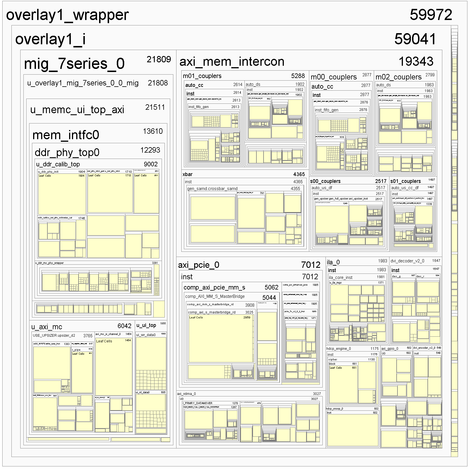
As a result, the Vivado tool is pretty bad at optimizing designs for area. For example, the PCI express core – while extremely configurable and well-vetted – has no way to turn off the AXI slave bridge, even if you’re not using the interface. Even with the inputs unconnected or tied to ground, the logic optimizer won’t remove the unused gates. Unfortunately, this piece of dead logic consumes around 20% of my target FPGA’s capacity. I could only reclaim that space by hand-editing the machine-generated VHDL to comment out the slave bridge. It’s a simple enough thing to do, and it had no negative effects on the core’s functionality. But Xilinx has no incentive to add a GUI switch to disable the logic, because the extra gates encourage you to “upgrade” by one FPGA size if your design uses a PCI express core. Similarly, the DDR3 memory core devotes 70% of its substantial footprint to a “calibration” block. Calibration typically runs just once at boot, so the logic is idle during normal operation. With an FPGA, the smart thing to do would be to run the calibration, store the values, and then jam the pre-measured values into the application design, thus eliminating the overhead of the calibration block. However, I couldn’t implement this optimization since the DDR3 block is provided as an opaque netlist. Finally, the AXI fabric automation – while magical – scales poorly with the number of ports. In my most recent benchmark design done with Vivado, 50% of the chip is devoted to the routing fabric, 25% to the DDR3 block, and the remainder to my actual application logic.

Tim mentioned that he thought the same design when using LiteX would fit in a much smaller FPGA. He has been using LiteX to generate the FPGA “gateware” (bitstreams) to support his HDMI2USB video processing pipelines on various platforms, ranging from the Numato-Opsis to the Atlys, and he even started a port for the NeTV2. Intrigued, I decided to port one of my Vivado designs to LiteX so that I could do an apples-to-apples comparison of the two design flows.

LiteX is a soft-fork of Migen/MiSoC – a python-based framework for managing hardware IP and auto-generating HDL. The IP blocks within LiteX are completely open source, and so can be targeted across multiple FPGA architectures. However, for low-level synthesis, place & route, and bitstream generation, it still relies upon proprietary chip-specific vendor tools, such as Vivado when targeting Artix FPGAs. It’s a little bit like an open source C compiler that spits out assembly, so it still requires vendor-specific assemblers, linkers, and binutils. While it may seem backward to open the compiler before the assembler, remember that for software, an assembler’s scope of work is simple — primarily within well-defined 32-bit or so opcodes. However, for FPGAs, the “assembler” (place and route tool) has the job of figuring out where to place single-bit primitives within an “opcode” that’s effectively several million bits long, with potential cross-dependencies between every bit. The abstraction layers, while parallel, aren’t directly comparable.

Let me preface my experience with the statement that I have a love-hate relationship with Python. I’ve used Python a few times for “recreational” projects and small tools, and for driving bits of automation frameworks. But I’ve found Python to be terribly frustrating. If you can use their frameworks from the ground-up, it’s intuitive, fun, even empowering. But if your application isn’t naturally “Pythonic”, woe to you. And I have a lot of needs for bit-banging, manipulating binary files, or grappling with low-level hardware registers, activities that are decidedly not Pythonic. I also spend a lot of time fighting with the “cuteness” of the Python type system and syntax: I’m more of a Rust person. I like strictly typed languages. I am not fond of novelties like using “-1” as the last-element array index and overloading the heck out of binary operators using magic methods.


Comics courtesy of xkcd, CC BY-NC-2.5

Surprisingly, I was able to get LiteX up and running within a day. This is thanks in large part to Tim’s effort to create a really comprehensive bootstrapping script that checks out the git repo, all of the submodules (thank you!), and manages your build environment. It just worked; the only bump I encountered was a bit of inconsistent documentation on installing the Xilinx toolchain (for Artix builds you need to grab Vivado; and Spartan you grab ISE). The whole thing ate about 19GiB of hard drive space, of which 18GiB is the Vivado toolchain.

I was rewarded with a surprisingly powerful and mature framework for defining SoCs. Thanks to the extensive work of the MiSoC and LiteX crowd, there’s already IP cores for DRAM, PCI express, ethernet, video, a softcore CPU (your choice of or1k or lm32) and more. To be fair, I haven’t been able to load these on real hardware and validate their spec-compliance or functionality, but they seem to compile down to the right primitives so they’ve got the right shape and size. Instead of AXI, they’re using Wishbone for their fabric. It’s not clear to me yet how bandwidth-efficient the MiSoC fabric generator is, but the fact that it’s already in use to route 4x HDMI connections to DRAM on the Numato-Opsis would indicate that it’s got enough horsepower for my application (which only requires 3x HDMI connections).

As a high-level framework, it’s pretty magical. Large IP instances and corresponding bus ports are allocated on-demand, based on a very high level description in Python. I feel a bit like a toddler who has been handed a loaded gun with the safety off. I’m praying the underlying layers are making sane inferences. But, at least in the case of LiteX, if I don’t agree with the decisions, it’s open source enough that I could try to fix things, assuming I have the time and gumption to do so.

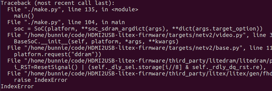
For my tool flow comparison, I implemented a simple 2x HDMI-in to DDR3 to 1x HDMI-out design in both Vivado and in LiteX. Creating the designs is about the same effort on both flows – once you have the basic IP blocks, instantiating bus fabric and allocation of addressing is largely automated in each case. Vivado is superior for pin/package layout thanks to its graphical planning tool (I find an illustration of the package layout to be much more intuitive than a textual list of ball-grid coordinates), and LiteX is a bit faster for design creation despite the usual frustrations I have with Python (up to the reader’s bias to decide whether it’s just that I have a different way of seeing things or if my intellect is insufficient to fully appreciate the goodness that is Python).


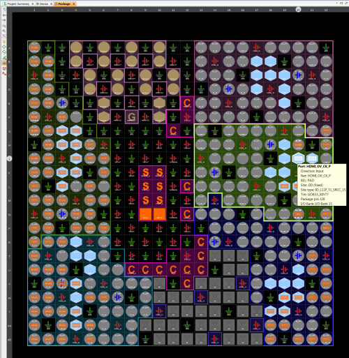
Pad layout planning in Vivado is aided by a GUI


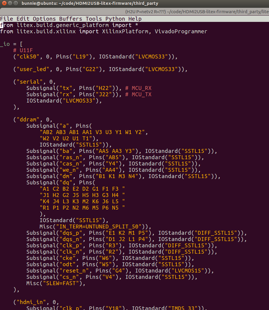
Example of LiteX syntax for pin constraints

But from there, the experience between the two diverges rapidly. The main thing that’s got me excited about LiteX is the speed and efficiency of its high-level synthesis. LiteX produces a design that uses about 20% of an XC7A50 FPGA with a runtime of about 10 minutes, whereas Vivado produces a design that consumes 85% of the same FPGA with a runtime of about 30-45 minutes.

Significantly, LiteX tends to “fail fast”, so syntax errors or small problems with configurations become obvious within a few seconds, if not a couple minutes. However, Vivado tends to “fail late” – a small configuration problem may not pop up until about 20 minutes into the run, due to the clumsy way it manages out-of-context block synthesis and build dependencies. This means that despite my frustrations with the Python syntax, the penalty paid for small errors is much less in terms of time – so overall, I’m more productive.

But the really compelling point is the efficiency. The fact that LiteX generates more efficient HDL means I can potentially shave a significant amount of cost out of a design by going to a smaller FPGA. Remember, both LiteX and Vivado use the same back-end for low-level sythesis and place and route. The difference is entirely in the high-level design automation – and this is a level that I can see being a good match for a Python-based framework. You’re not really designing hardware with Python (eventually it all turns into Verilog) so much as managing and configuring libraries of IP, something that Python is quite well suited for. To wit, I dug around in the MiSoC libraries a bit and there seem to be some serious logic designs using this Python syntax. I’m not sure I want to wrap my head around this coding style, but the good news is I can still write my leaf cells in Verilog and call them from the high-level Python integration framework.

So, I’m cautiously proceeding to use LiteX as the main design flow going forward for NeTV2. We’ll see how the bitstream proves out in terms of timing and functionality once my next generation hardware is available, but I’m optimistic. I have a few concerns about how debugging will work – I’ve found the Xilinx ILA cores to be extremely powerful tools and the ability to automatically reverse engineer any complex design into a schematic (a feature built into Vivado) helps immensely with finding timing and logic bugs. But with a built-in soft CPU core, the “LiteScope” logic analyzer (with sigrok support coming soon), and fast build times, I have a feeling there is ample opportunity to develop new, perhaps even more powerful methods within LiteX to track down tricky bugs.

My final thought is that LiteX, in its current state, is probably best suited for people trained to write software who want to design hardware, rather than for people classically trained in circuit design who want a tool upgrade. The design idioms and intuitions built into LiteX pulls strongly from the practices of software designers, which means a lot of “obvious” things are left undocumented that will throw outsiders (e.g. hardware designers like me) for a loop. There’s no question about the power and utility of the design flow – so, as the toolchain matures and documentation improves I’m optimistic that this could become a popular design flow for hardware projects of all magnitudes.


Interested? Tim has suggested the following links for further reading:

NeTV2 FPGA Reference Design

Saturday, December 3rd, 2016

A complex system like NeTV2 consists of several layers of design. About a month ago, we pushed out the PCB design. But a PCB design alone does not a product make: there’s an FPGA design, firmware for the on-board MCU, host drivers, host application code, and ultimately layers in the cloud and beyond. We’re slowly working our way from the bottom up, assembling and validating the full system stack. In this post, we’ll talk briefly about the FPGA design.

This design targets an Artix-7 XC7A50TCSG325-2 FPGA. As such, I opted to use Xilinx’s native Vivado design flow, which is free to download and use, but not open source. One of Vivado’s more interesting features is a hybrid schematic/TCL design flow. The designs themselves are stored as an XML file, and dynamically rendered into a schematic. The schematic itself can then be updated and modified by using either the GUI or TCL commands. This hybrid flow strikes a unique balance between the simplicity and intuitiveness of designing with a schematic, and the power of text-based scripting.


Above: top-level schematic diagram of the NeTV2 FPGA reference design as rendered by the Vivado tools

However, the main motivation to use Vivado is not the design entry methodology per se. Rather, it is Vivado’s tight integration with the AXI IP bus standard. Vivado can infer AXI bus widths, address space mappings, and interconnect fabric topology based on the types of blocks that are being strung together. The GUI provides some mechanisms to tune parameters such as performance vs. area, but it’s largely automatic and does the right thing. Being able to mix and match IP blocks with such ease can save months of design effort. However, the main downside of using Vivado’s native IP blocks is they are area-inefficient; for example, the memory-mapped PCI express block includes an area-intensive slave interface which is synthesized, placed, and routed — even if the interface is totally unused. Fortunately many of the IP blocks compile into editable verilog or VHDL, and in the case of the PCI express block the slave interface can be manually excised after block generation, but prior to synthesis, reclaiming the logic area of that unused interface.

Using Vivado, I’m able to integrate a PCI-express interface, AXI memory crossbar, and DDR3 memory controller with just a few minutes of effort. With similar ease, I’ve added in some internal AXI-mapped GPIO pins to provide memory-mapped I/O within the FPGA, along with a video DMA master which can format data from the DDR3 memory and stream it out as raster-synchronous RGB pixel data. All told, after about fifteen minutes of schematic design effort I’m positioned to focus on coding my application, e.g. the HDMI decode/encode, HDCP encipher, key extraction, and chroma key blender.

Below is the “hierarchical” view of this NeTV2 FPGA design. About 75% of the resources are devoted to the Vivado IP blocks, and about 25% to the custom NeTV application logic; altogether, the design uses about 72% of the XC7A50T FPGA’s LUT resources. A full-custom implementation of the Vivado IP blocks would save a significant amount of area, as well as be more FOSS-friendly, but it would also take months to implement an equivalent level of functionality.

Significantly, the FPGA reference design shared here implements only the “basic” NeTV chroma-key based blending functionality, as previously disclosed here. Although we would like to deploy more advanced features such as alpha blending, I’m unable to share any progress because this operation is generally prohibited under Section 1201 of the DMCA. With the help of the EFF, I’m suing the US government for the right to disclose and share these developments with the general public, but until then, my right to express these ideas is chilled by Section 1201.

NeTV2 Tech Details Live

Tuesday, November 1st, 2016

Alphamax LLC now has details of the NeTV2 live, including links to preliminary schematics and PCB source files.

The key features of NeTV2 include:

  • mPCIE v2.0 (5Gbps x1 lane) add-in card format
  • Support for full 1080p60 video
  • Artix-7 FPGA
  • FPGA “hack port” breaking out 3x spare GTP transceiver pairs
  • 512 MB of DDR3-800 @ 32-bit wide memory for frame buffering

I adopted an add-in card format to allow end users to pick the cost/performance trade-off that suited their application the best. Some users require only a text overlay (NeTV’s original design scenario); but others wanted to blend HD video and 3D graphics, which would require a substantially more powerful and expensive CPU. An add-in card allows users to plug into anything from an economical $60 all-in-one, to a fully loaded gaming machine. The kosagi forum has an open thread for NeTV2 discussion.

As noted previously, we are currently seeking legal clarity on the suite of planned features for the product, including highly requested features such as alpha blending which require access to the descrambled video stream.