Archive for the ‘The Factory Floor’ Category

Fixing a Tiny Corner of the Supply Chain

Tuesday, December 14th, 2021

No product gets built without at least one good supply chain war story – especially true in these strange times. Before we get into the details of the story, I feel it’s worth understanding a bit more about the part that caused me so much trouble: what it does, and why it’s so special.

The Part that Could Not Be Found
There’s a bit of magic in virtually every piece of modern electronics involved in the generation of internal timing signals. It’s called an oscillator, and typically it’s implemented with a precisely cut fleck of quartz crystal that “rings” when stimulated, vibrating millions of times per second. The accuracy of the crystal is measured in parts-per-million, such that over a month – about 2.5 million seconds – a run-of-the-mill crystal with 50ppm accuracy might drift by about two minutes. In mechanical terms it’s like producing 1kg (2.2 pound) bags of rice that have precisely no more and no less than one grain of rice compared to each other; or in CS terms it’s about 15 bits of precision (it’s funny how one metric sounds hard, while the other sounds trivial).

One of the many problems with quartz crystals is that they are big. Here’s a photo from wikipedia of the inside of a typical oscillator:


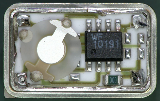
CC BY-SA 4.0 by Binarysequence via Wikipedia

The disk on the left is the crystal itself. Because the frequency of the crystal is directly related to its size, there’s a “physics limit” on how small these things can be. Their large size also imposes a limit on how much power it takes to drive them (it’s a lot). As a result, they tend to be large, and power-hungry – it’s not uncommon for a crystal oscillator to be specified to consume a couple milliamperes of current in normal operation (and yes, there are also chips with built-in oscillator circuits that can drive crystals, which reduces power; but they, too, have to burn the energy to charge and discharge some picofarads of capacitance millions of times per second due to the macroscopic nature of the crystal itself).

A company called SiTime has been quietly disrupting the crystal industry by building MEMS-based silicon resonators that can outperform quartz crystals in almost every way. The part I’m using is the SiT8021, and it’s tiny (1.5×0.8mm), surface-mountable (CSBGA), consumes about 100x less power than the quartz-based competition, and has a comparable frequency stability of 100ppm. Remarkably, despite being better in almost every way, it’s also cheaper – if you can get your hands on it. More on that later.

Whenever something like this comes along, I always like to ask “how come this didn’t happen sooner?”. You usually learn something interesting in exploring that question. In the case of pure-silicon oscillators, they have been around forever, but they are extremely sensitive to temperature and aging. Anyone who has designed analog circuits in silicon are familiar with the problem that basically every circuit element is a “temperature-to-X” converter, where X is the parameter you wish you could control. For example, a run of the mill “ring oscillator” with no special compensation would have an initial frequency accuracy of about 50% – going back to our analogies, it’d be like getting a bag of rice that nominally holds 1kg, but is filled to an actual weight of somewhere between 0.5kg and 1.5kg – and you would get swings of an additional 30% depending upon the ambient temperature. A silicon MEMS oscillator is a bit better than that, but its frequency output would still vary wildly with temperature; orders of magnitude more than the parts-per-million specified for a quartz crystal.

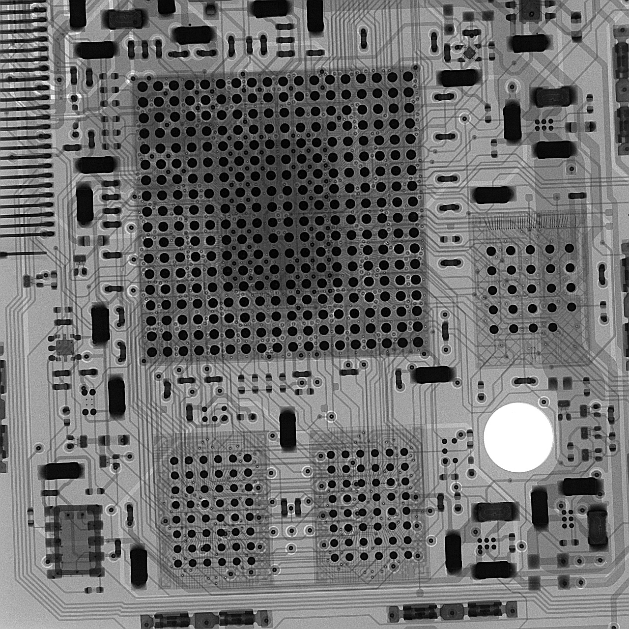
So, how do they turn something so innately terrible into something better-than-quartz? First I took a look at the devices under a microscope, and it’s immediately obvious that it’s actually two chips that have been bonded face-to-face with each other.


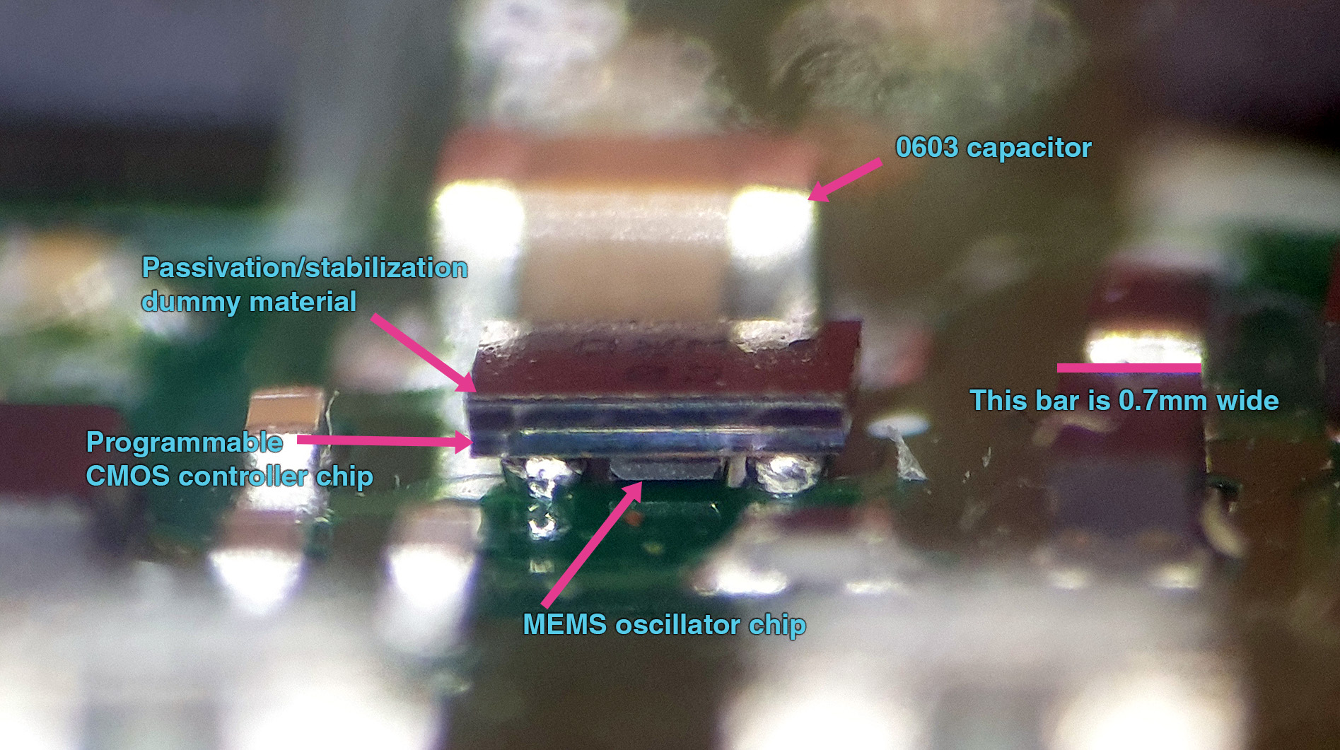
Edge-on view of an SiT8021 already mounted on a circuit board.

I deduced that a MEMS oscillator chip is nestled between the balls that bond the chip to the PCB. I did a quick trawl through the patents filed by SiTimes, and I’m guessing the MEMS oscillator chip contains at least two separate oscillators. These oscillators are intentionally different, so that their frequency drift with temperature also have different, but predictable, curves. They can use the relative difference of the frequencies to very precisely measure the absolute temperature of the pair of oscillators by comparing the instantaneous difference between the two frequencies. In other words, they took the exact problem that plagues silicon designs, and turned it into a feature: they built a very precise temperature sensor out of two silicon oscillators.

With the temperature of the oscillators known to exquisite precision, one can now compensate for the temperature effects. That’s what the larger of the two chips (the one directly attached to the solder balls) presumably does. It computes an inverse mapping of temperature vs. frequency, constantly adjusting a PLL driven by one of the two MEMs oscillators, to derive a precise, temperature-stable net frequency. The controller chip presumably also contains a set of eFuses that are burned in the factory (or by the distributor) to calibrate and set the initial frequency of the device. I didn’t do an acid decap of the controller chip, but it’s probably not unreasonable for it to be fabricated in 28nm silicon; at this geometry you could fit an entire RISC-V CPU in there with substantial microcode and effectively “wrap a computer” around the temperature drift problem that plagues silicon designs.

Significantly, the small size of the MEMS resonator compared to a quartz crystal, along with its extremely intimate bonding to the control electronics, means a fundamentally lower limit on the amount of energy required to sustain resonance, which probably goes a long way towards explaining why this circuit is able to reduce active power by so much.

The tiny size of the controller chip means that a typical 300mm wafer will yield about 50,000 chips; going by the “rule of thumb” that a processed wafer is roughly $3k, that puts the price of a raw, untested controller chip at about $0.06. The MEMs device is presumably a bit more expensive, and the bonding process itself can’t be cheap, but at a “street price” of about $0.64 each in 10k quantities, I imagine SiTime is still making good margin. All that being said, a million of these oscillators would fit on about 18 wafers, and the standard “bulk” wafer cassette in a fab holds 25 wafers (and a single fab will pump out about 25,000 – 50,000 wafers a month); so, this is a device that’s clearly ready for mobile-phone scale production.

Despite the production capacity, the unique characteristics of the SiT8021 make it a strong candidate to be designed into mobile phones of all types, so I would likely be competing with companies like Apple and Samsung for my tiny slice of the supply chain.

The Supply Chain War Story
It’s clearly a great part for a low-power mobile device like Precursor, which is why I designed it into the device. Unfortunately, there’s also no real substitute for it. Nobody else makes a MEMS oscillator of comparable quality, and as outlined above, this device is smaller and orders of magnitude lower power than an equivalent quartz crystal. It’s so power-efficient that in many chips it is less power to use this off-chip oscillator, than to use the built-in crystal oscillator to drive a passive crystal. For example, the STM32H7 HSE burns 450uA, whereas the SiT8021 runs at 160uA. To be fair, one also has to drive the pad input capacitance of the STM32, but even with that considered you’re probably around 250uA.

To put it in customer-facing terms, if I were forced to substitute commonly available quartz oscillators for this part, the instant-on standby time of a Precursor device would be cut from a bit over 50 hours down to about 40 hours (standby current would go from 11mA up to 13mA).

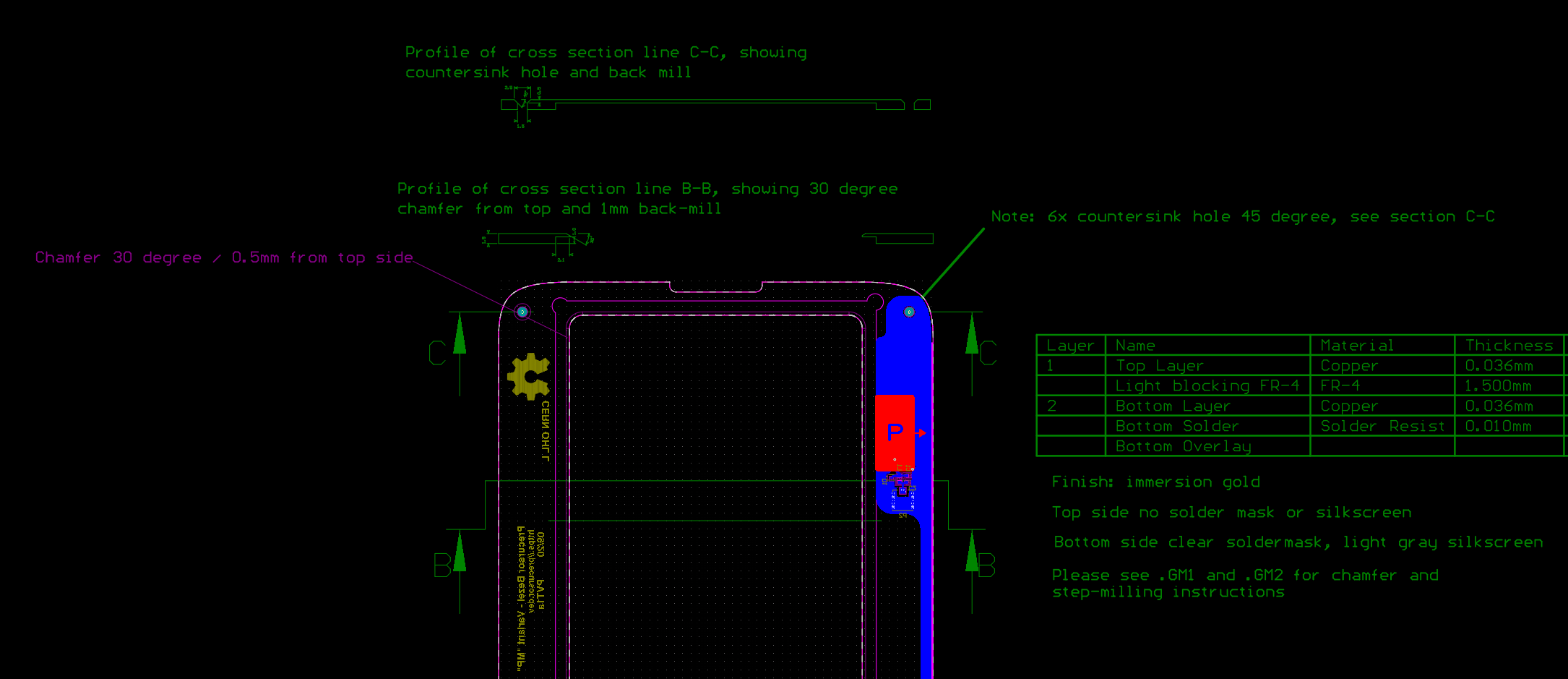
If this doesn’t make the part special enough, the fact that it’s an oscillator puts it in a special class with respect to electromagnetic compliance (EMC) regulations. These are the regulations that make sure that radios don’t interfere with each other, and like them or not, countries take them very seriously as trade barriers – by requiring expensive certifications, you’re able to eliminate the competition of small upstarts and cheap import equipment on “radio safety” grounds. Because the quality of radio signals depend directly upon the quality of the oscillator used to derive them, the regulations (quite reasonably) disallow substitutions of oscillators without re-certification. Thus, even if I wanted to take the hit on standby time and substitute the part, I’d have to go through the entire certification process again, at a cost of several thousand dollars and some weeks of additional delay.

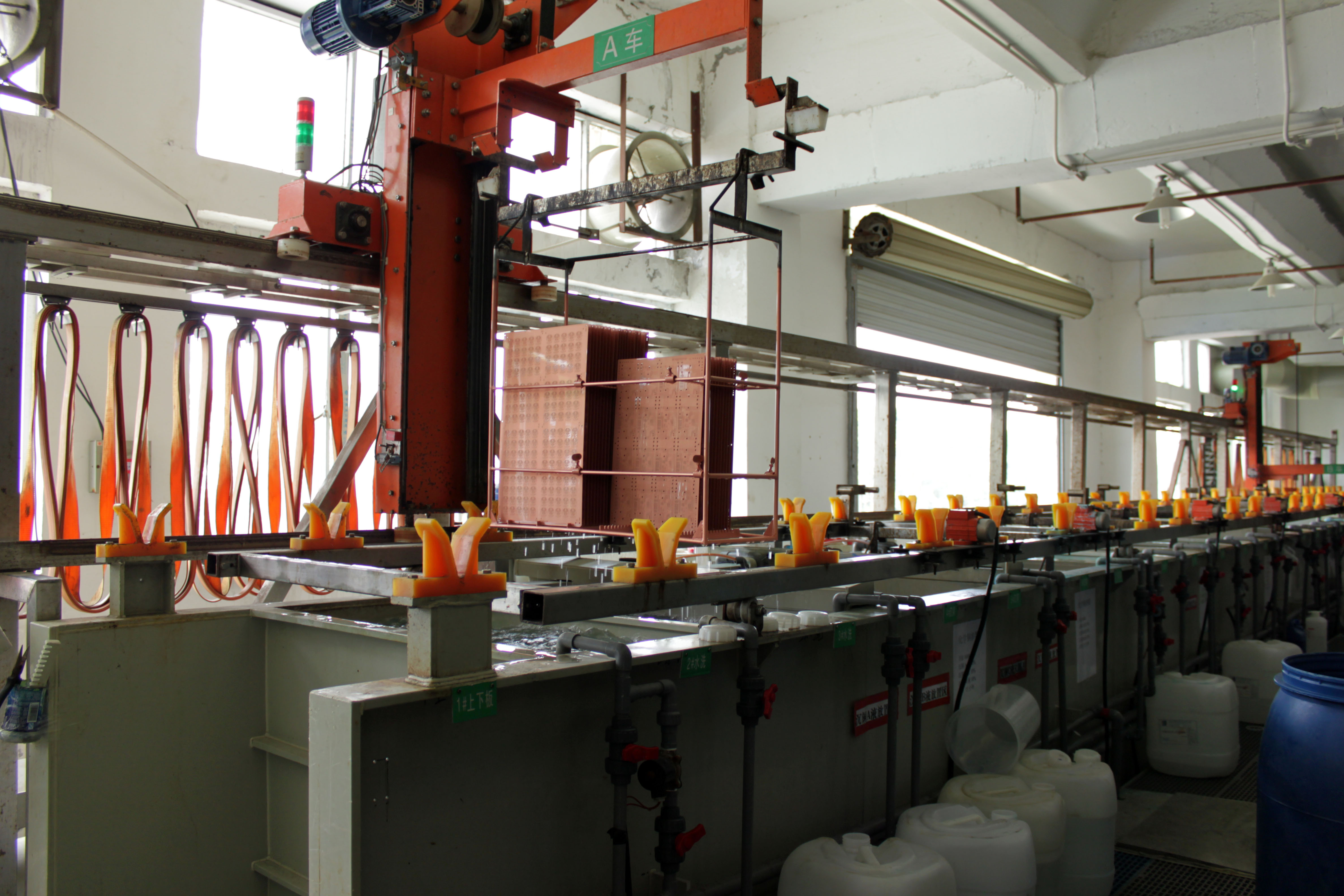
Thus this part, along with the FPGA, is probably one of the two parts on the entire BOM that I really could not do without. Of course, I focused a lot on securing the FPGA, because of its high cost and known difficulty to source; but for want of a $0.68 crystal, a $565 product would not be shipped…

The supply chain saga starts when I ordered a couple thousand of these in January 2021, back when it had about a 30 week lead time, giving a delivery sometime in late August 2021. After waiting about 28 weeks, on August 12th, we got an email from our distributor informing us that they had to cancel our entire order for SiT8021s. That’s 28 weeks lost!

The nominal reason given was that the machine used to set the frequency of the chips was broken or otherwise unavailable, and due to supply chain problems it couldn’t be fixed anytime soon. Thus, we had to go to the factory to get the parts. But, in order to order direct from the factory, we had to order 18,000 pieces minimum – over 9x of what I needed. Recall that one wafer yields 58,000 chips, so this isn’t even half a wafer’s worth of oscillators. That being said, 18,000 chips would be about $12,000. This isn’t chump change for a project operating on a fixed budget. It’s expensive enough that I considered recertification of the product to use a different oscillator, if it weren’t for the degradation in standby time.

Panic ensues. We immediately trawl all the white-market distributor channels and buy out all the stock, regardless of the price. Instead of paying our quoted rate of $0.68, we’re paying as much as $1.05 each, but we’re still short about 300 oscillators.

I instruct the buyers to search the gray market channels, and they come back with offers at $5 or $6 for the $0.68 part, with no guarantee of fitness or function. In other words, I could pay 10x of the value of the part and get a box of bricks, and the broker could just disappear into the night with my money.

No deal. I had to do better.

By this time, every distributor was repeating the “18k Minimum Order Quantity (MOQ) with long lead time” offer, and my buyers in China waved the white flag and asked me to intervene. After trawling the Internet for a couple hours, I discover that Element14 right here in Singapore (where I live) claims to be able to deliver small quantities of the oscillator before the end of the year. It seems too good to be true.

I ask my buyers in China to place an order, and they balk; the China office repeats that there is simply no stock. This has happened before, due to trade restrictions and regional differences the inventory in one region may not be orderable in another, so I agree to order the balance of the oscillators with a personal credit card, and consign them directly to the factory. At this point, Element14 is claiming a delivery of 10-12 weeks on the Singapore website: that would just meet the deadline for the start of SMT production at the end of November.

I try to convince myself that I had found the solution to the problem, but something smelled rotten. A month later, I check back into the Element14 website to see the status of the order. The delivery had shifted back almost day-for-day to December. I start to suspect maybe they don’t even carry this part, and it’s just an automated listing to honeypot orders into their system. So, I get on the phone with an Element14 representative, and crazy enough, she can’t even find my order in her system even though I can see the order in my own Element14 account. She tells me this is not uncommon, and if she can’t see it in her system, then the web order will never be filled. I’m like, is there any way you can cancel the order then? She’s like “no, because I can’t see the order, I can’t cancel it.” But also because the representative can’t see the order, it also doesn’t exist, and it will never be filled. She recommends I place the order again.

I’m like…what the living fuck. Now I’m starting to sweat bullets; we’re within a few weeks of production start, and I’m considering ordering 18,000 oscillators and reselling the excess as singles via Crowd Supply in a Hail Mary to recover the costs. The frustrating part is, the cost of 300 parts is small – under $200 – but the lack of these parts blocks the shipment of roughly $170,000 worth of orders. So, I place a couple bets across the board. I go to Newark (Element14, but for the USA) and place an order for 500 units (they also claimed to be able to deliver), and I re-placed the order with Element14 Singapore, but this time I put a Raspberry Pi into the cart with the oscillators, as a “trial balloon” to test if the order was actually in their system. They were able to ship the part of the order with the Raspberry Pi to me almost immediately, so I knew they couldn’t claim to “lose the order” like before – but the SiT8021 parts went from having a definitive delivery date to a “contact us for more information” note – not very useful.

I also noticed that by this time (this is mid-October), Digikey is listing most of the SiT8021 parts for immediately delivery, with the exception of the 12MHz, 1.8V version that I need. Now I’m really starting to sweat – one of the hypothesis pushed back at my by the buyer in China was that there was no demand for this part, so it’s been canceled and that’s why I can’t find it anywhere. If the part’s been canceled, I’m really screwed.

I decide it’s time to reach out to SiTime directly. Through hook and crook, I get in touch with a sales rep, who confirms with me that the 12MHz, 1.8V version is a valid and orderable part number, and I should be able to go to Digikey to purchase it. I inform the sales rep that the Digikey website doesn’t list this part number, to which they reply “that’s strange, we’ll look into it”.

Not content to leave it there, I reach out to Digikey directly. I get connected to one of their technical sales representatives via an on-line chat, and after a bit of conversing, I confirmed that in fact the parts are shipped to Digikey as blanks, and they have a machine that can program the parts on-site. The technical sales rep also confirms the machine can program that exact configuration of the part, but because the part is not listed on the website I have to do a “custom part” quotation.

Aha! Now we are getting somewhere. I reach out to their custom-orders department and request a quotation. A lady responds to me fairly quickly and says she’ll get back to me. About a week passes, no response. I ping the department again, no response.

“Uh-oh.”

I finally do the “unthinkable” in the web age – I pick up the phone, and dial in hoping to reach a real human being to plead my case. I dial the extension for the custom department sales rep. It drops straight to voice mail. I call back again, this time punching the number to draw a lottery ticket for a new sales rep.

Luckily, I hit the jackpot! I got connected with a wonderful lady by the name of Mel who heard out my problem, and immediately took ownership for solving the problem. I could hear her typing queries into her terminal, and hemming and hawing over how strange it is for there to be no order code, but she can still pull up pricing. While I couldn’t look over her shoulder, I could piece together that the issue was a mis-configuration in their internal database. After about 5 minutes of tapping and poking, she informs me that she’ll send a message to their web department and correct the issue. Three days later, my part (along with 3 other missing SKUs) is orderable on Digikey, and a week later I have the 300 missing oscillators delivered directly to the factory – just in time for the start of SMT production.

I wrote Mel a hand-written thank-you card and mailed it to Digikey. I hope she received it, because people like here are a rare breed: she has the experience to quickly figure out how the system breaks, the judgment to send the right instructions to the right groups on how to fix it, and the authority to actually make it happen. And she’s actually still working a customer-facing job, not promoted into a corner office management position where she would never be exposed to a real-world problem like mine.

So, while Mel saved my production run, the comedy of errors still plays on at Element14 and Newark. The “unfindable order” is still lodged in my Element14 account, probably to stay there until the end of time. Newark’s “international” department sent me a note saying there’s been an export compliance issue with the part (since when did jellybean oscillators become subject to ITAR restrictions?!), so I responded to their department to give them more details – but got no response back. I’ve since tried to cancel the order, got no response, and now it just shows a status of “red exclamation mark” on hold and a ship date of Jan 2022. The other Singapore Element14 order that was combined with the Raspberry Pi still shows the ominous “please contact us for delivery” on the ship date, and despite trying to contact them, nobody has responded to inquiries. But hey, Digikey’s Mel has got my back, and production is up and (mostly) running on schedule.

This is just is one of many supply chain war stories I’ve had with this production run, but it is perhaps the one with the most unexpected outcome. I feared that perhaps the issue was intense competition for the parts making them unavailable, but the ground truth turned out to be much more mundane: a misconfigured website. Fortunately, this small corner of the supply chain is now fixed, and now anyone can buy the part that caused me so many sleepless nights.

Precursor’s Mechanical Design

Monday, December 7th, 2020

“Pocketability” is the difference between Precursor and naked PCB FPGA development platforms. We hope Precursor’s pocketability helps bring more open hardware out of the lab and into everyday use. Thus, the mechanical design of Precursor is of similar importance to its electrical, software, and security design.

We always envisioned Precursor as a device that complements a smartphone. In fact, some of the earliest sketches had Precursor (then called Betrusted) designed into a smartphone’s protective case. In this arrangement, Precursor would tether to the phone via WiFi and the always-on LCD for Precursor could then be used to display static data, such as a shopping list or a QR code for a boarding pass, giving Precursor a bit of extra utility as a second screen that’s physically attached to your phone. However, there are too many types of smartphones out there to make “Precursor as a phone case” practical, so we realized it would make more sense to make Precursor a “stand-alone device”.

As such, we wanted Precursor to be unobtrusive and thin in order to lighten the burden of carrying a secondary security device. Our first-draft EVT design had Precursor at just 5.7 mm thick, placing it among the ranks of the thinnest phones. Unfortunately, the EVT device had no backlight on the LCD, which made it unusable in low-light conditions. Increasing the final thickness to 7.2 mm allowed us to introduce a backlight, while still being slimmer than every iPhone since the iPhone 8.

To minimize the thickness of Precursor, I first divided the design into major zones, such as the main electronics area, the battery compartment, the vibration motor, and the speaker. I then estimated the overall thickness of components in each zone and optimized the thickest one by either re-arranging components or making component substitutions until another zone dominated the overall thickness.


A cross-section view of the final Precursor design, calling out the dimensions of the various vertical height zones of the design.

After considering about a dozen or so mechanical layout scenarios, we arrived at the design shown above. Like every modern mobile device, when viewed by size and weight, Precursor is basically a battery attached to a display.

The practical limit on battery thickness is driven by the overhead of the protective wrapping around the battery. Lithium-polymer “pouch” batteries rapidly decline in energy density with decreasing thickness as the protective wrapper around the battery starts to factor appreciably into its overall thickness. The loss of energy density becomes appreciable below 3.5mm, and so this fixed the battery’s thickness at 3.5mm, plus about 0.2mm allowance for any swelling that might happen plus adhesive films.


Teardown view of Precursor’s LCD with backlight attached. Note that to inspect the transistors inside the LCD, the backlight module needs to be removed.

Display thickness is limited by the thickness of the liquid crystal (LC) “cell”, plus backlight. Fortunately, LC cells are extremely thin, as they are basically just the glass sheets used to confine a microscopic layer of liquid crystal material, plus some polarizer films – in Precursor’s case, the LC cell is just 0.705mm thick. The backlight is substantially thicker, as it requires a waveguide plus a film stack that consists of two brightness enhancing films, a diffuser sheet, adhesives, and its own protective case to hold the assembly together, leading to a net thickness increase of roughly 1.3mm. The backlight itself is actually a full-custom assembly that we designed just for Precursor; it’s not available as an off-the-shelf part.

With the display and battery thicknesses defined, the final thickness of the product is determined by the material selection of the protective case. We use aluminum for the bottom case and FR-4 for the bezel (we discuss the bezel in a previous post).

Using aluminum for the bottom case allows us to shave about 1 mm (~15%) of thickness relative to using a polymer like ABS or PC at the expense of a fairly substantial increase in per-unit manufacturing costs. Although polymers are about twice the cost of aluminum by weight, an aluminum case costs about 10x as much to produce. This is because polymers can be molded in a matter of seconds, with very little waste material, whereas aluminum must be CNC’d out of a slab in a time-consuming process that scraps 80% of the original material. Surprisingly, the 10x cost-up isn’t the waste material; there is an efficient market for buying and recycling post-machining aluminum. Most of the extra cost is due to the labor required to machine the case which is orders of magnitude longer than the time required for injection molding.

Thus, while we could have made Precursor cheaper, we felt it would both be more pocketable, as well as more desirable, with the machined aluminum case: it would look more like a high-end mobile device, instead of a cheap plastic toy or remote control.

Using aluminum also allows us to play some fun tricks with the fit and finish of the product, thanks in part to the transformative effect Apple had on the mobile phone industry. Their adoption of CNC machining as a mass production process sparked a huge investment in CNC capability, making once-exotic processes more affordable for everyone. A good example of this is the single-crystal diamond cutting process for making shiny beveled edges. This used to be a fairly expensive specialty process, which you can read more about in this great thesis on “Precision and Techniques for Designing Precision Machines” by Layton Carter Hale which, on page 27, describes the Large Optics Diamond Turning Machine (LODTM). The LODTM relies on the raw precision achievable with a diamond bit to create geometries for mirrors without the need for post-polishing.


A single-crystal diamond bit, courtesy of Victor from Jiada

I first learned about this technique in 2017, when I brought a Xiaomi aluminum mouse pad with a mirror-finish bevel.


Bevel on the Xiaomi mousepad

Despite a sub-$20 price tag, the mirror-finish bevel gave it quite an expensive look. Polishing to a mirror finish is a time consuming task, so I became curious about how this could be economical on a humble mouse pad. I bought another mouse pad, and brought it to Prof. Nadya Peek, and asked her how she thought it was fabricated. Readers who are familiar with our Novena laptop may recall her name as the designer of the Peek Array for mounting accessories inside the Novena. I’ve been lucky to have her mentorship and advice on all things mechanical engineering for many years now. So many of my products are better thanks to her!

She took one look at the bevel and immediately guessed it was cut by a single-crystal diamond bit, but she could do even better than making a guess. At the time, she was still a graduate student at the MIT Center for Bits and Atoms, where she had a Hitachi FlexSEM 1000 II equipped with the X-ray composition analysis option at her disposal. So, she took the mouse pad to the machine shop, chopped a corner off with a band saw, and loaded it into the SEM.


Viewing the output of the composition analysis.

If you zoom into the screen on the right, you can see the X-ray composition analysis reveals an unusually high amount of carbon on the aluminum surface (~10% by weight). Unlike iron, carbon is not commonly used in alloying aluminum. In this case, the chief alloying element seems to be magnesium, implying that the mousepad is probably a 5000-series alloy (perhaps 5005 or 5050). Given this, it seemed reasonable to conclude that the carbon residue on the beveled surface is direct evidence of a diamond cutting bit.


The shiny beveled edge on Precursor is brought to you by a single-crystal diamond milling bit.

Armed with this knowledge, I was able to work with Victor, the owner of Jiada – the primary CNC provider for Precursor – to specify a diamond-bit beveling process that brings you the nice edge finish on the final Precursor product. I also count Victor as one of my many mechanical design mentors; he’s one of those practicing-engineer-as-CEO types who has applied his extensive knowledge of mechanical engineering to open his own CNC and injection molding business. He always seems up for the challenge of developing new and interesting fabrication processes. That’s why I’ve been working closely with Victor to develop the campaign-only omakase version of Precursor.

Because Precursor’s case is CNC, we’re not limited to aluminum as the base material. It’s primarily a matter of cost and yield to manufacture with other materials. We could, for example, machine the case out of titanium, but the difficulty of machining titanium means we would likely have to machine two or three cases to yield a single one that passes all of our quality standards. This, combined with the high cost of raw titanium, would have added about a thousand dollars on to the final price of the omakase Precursor and we felt that would be just too expensive. Thus, Victor and I are currently evaluating two material candidates: one is physical vapor deposition (PVD)-finished stainless steel, the other is naval brass. These material choices were heavily influenced by Prof. Peek’s opinions. (It’s a coincidence the recently launched iPhone 12 uses PVD stainless steel for its case, as we have been working on this project since well before the details of iPhone 12 were publicly known.)

While both the PVD steel and naval brass are much more expensive than aluminum, they have a terrific hand feel and excellent machinability. Aesthetically, the main difference between the two is the color: for the stainless steel PVD, we’d be going with a high-gloss, polished black look, and for the naval brass we’re considering a brushed finish. The naval brass is more distinctive, but the soft metal is easy to scratch; a highly polished brass surface starts to look much less nice after a week or two of banging around in your pocket. A brushed finish hides such scratches and fingerprints better and over the course of years it should develop a handsome patina.

The major downside of the naval brass is that it’s highly conductive. Both the PVD stainless steel and anodized aluminum inherently have a tough, non-conductive surface layer; the naval brass does not. This is particularly concerning because if any of the internal battery connections get frayed, it could lead to a fire hazard. I’m currently working to see if I can find a surface coating that adequately protects the inside of the naval brass case from short circuits, but if I can’t find one, that may definitively rule out the naval brass option, leaving us with a PVD stainless steel case for the omakase version.

While good looks and a nice hand feel are significant benefits of going with a CNC process, another important reason I picked CNC over injection molding is anyone could build a full-custom version of a Precursor case in single quantities, with no compromise on finish quality or durability. Unlike the situation of injection molding versus 3D printing, which either use radically different base materials (for SLA 3D printing) or processes (for FDM 3D printing), your custom case can be made in single quantities with the exact same metal alloys and the exact same processes used in production Precursors.

This trait is particularly important for a mobile device and not just because the design works better when it’s built using its originally intended material system. It’s also because mobile devices don’t have a lot of extra space to devote to expansion headers and breakout boards. While it is beyond the level of a weekender hobby project to make a custom case, it’s probably within the scope of an undergraduate-level research project to undertake the necessary revisions to, for example, thicken the case and incorporate a novel medical sensor or a new kind of radio. In order to facilitate easier modifications to the case’s native Solidworks design file, I use a “master profile” to define the case body, bezel, and “ribbon” (the outer band that defines the height of the case). Helena Wang, another friend to whom I turn to for advice on mechanical design, taught me about the general technique of top-down modeling and using master profiles. Top-down modeling pushes a lot of design work into the up-front structure and planning of the 3D body in exchange for being able to revise the model without having to resolve dozens of conflicting downstream mechanical constraints. For example, when I realized I had to modify the case to be 1.5mm thicker to accommodate the backlight for the LCD, I was able to make the necessary change by just adjusting a single dimension in the ribbon height master profile, followed up by perhaps a half hour of cleaning up the offsets on structures which were defined outside of the master profile, such as the mounting points used to support the keyboard and the polymer radome that allows the WiFi signal out from the metal case.


A screenshot of the CAD tool view of the Precursor case, highlighting the master profile that defines the outer dimensions of the case.

Of course, making edits to the master profile requires access to a copy of Solidworks, which is not an open source tool; but FreeCAD users are welcome to redraw the design in their native format! I’ve heard good things about FreeCAD, but I just haven’t had the time to learn a new design tool. For smaller modifications that don’t involve changing major dimensions of the case – such as adding some extra through-holes for sensors or internal mounts for additional circuit boards – the case design is also available in a tool-neutral STEP format. Every CAD tool I know of can accept STEP format and, since it is actually the format used for CNC fabrication, it’s by definition sufficient for creating copies of the case.

If you’ve read my posts over the years, you may have noticed that I’ve never taken a formal course on mechanical engineering. Everything I know has been either gleaned from taking things apart, touring factories, scouring the Internet, and perhaps most importantly receiving advice from friends and mentors like Nadya, Victor, and Helena. It’s been a wonderful journey learning how things are made, I hope posts like this and the associated design files will aid anyone who wants to learn about mechanical design, so they may have an easier time of it than I did. Most of all, I’m hoping applying my experience and making Precursor pocketable and hackable will enable more open source technology to make it out of the lab and into everyday use, without requiring anyone to learn about mechanical design.

Thanks again to all our backers for bringing us closer to our funding goal! At the time of posting, we’re just at 90% funded, but we’re also getting down to the last week to wrap things up. We need your support to get us over the 100% mark. We recognize that these are difficult, trying times for everyone, but even small $10 donations inch us toward a successful campaign. Perhaps more importantly, if you know someone who might be interested in Precursor, we’d appreciate your help in spreading the word and letting them know about our campaign. With your help, hopefully we’ll blow past our funding goal before the campaign ends, and we can begin the hard but enjoyable work of building and delivering the first run of Precursor devices.

Precursor’s Custom PCBs

Tuesday, December 1st, 2020

While the last few updates about Precursor have focused on evidence-based trust and security, this update is more about the process of making Precursor itself. There is an essential link between evidence-based trust and understanding the manufacturing process: to convince yourself that something has been constructed correctly, it’s helpful to understand the construction process itself. It’s hard to tell if a small crack in a wall is the result of harmless foundation settling, or a harbinger of a building’s imminent collapse, without first understanding the function and construction of that wall.

Most designers like to abstract the PCB away as a commodity service, preferring “no-touch” or “one-click” ordering services where design files are uploaded and finished boards arrive in the mail, on time and at a good price. This is a bit like running a restaurant and ordering your produce from a mass distributor. The quality is uniform, delivery times are good, and the taste is acceptable. However, it’s hard to make a dish that’s really differentiated when basic ingredients all come from the same place.

I personally enjoy building electronics with a bit more of an artisanal flavor. Just as gourmet chefs invest the effort to develop relationships with their farmers, I’ve developed a personal relationship with my preferred PCB shop, King Credie. Since a PCB is at the core of virtually everything I build, I have found developing a healthy personal relationship with my PCB supplier has the benefit of raising the bar on virtually all my products. While King Credie is neither the cheapest nor the quickest-turn of PCB shops, their quality is consistent and, most importantly, they are willing to customize their process. For a small shop, they offer a wide variety of speciality processes, such as rigi-flex, metal core, edge plated cavities, HDI, and custom soldermask colors.

The Precursor Bezel

The bezel for Precursor, shown below, is a good example of how this flexibility can be used in practice. The front surface of Precursor is actually a raw FR-4 PCB while the Precursor logo is a 2.4GHz antenna. The two small black dots in the logo beneath the “P” are the antenna feed and ground stub vias, respectively, for a “PIFA” (planar inverse F)-style antenna. The PCB itself has been countersunk, beveled, and step-milled so it can function simultaneously as a mechanical bezel, an RF antenna, and a circuit board for electrical components.

Above is an inside shot of the bezel displaying step-milling and electrical circuitry on the inside surface of the bezel PCB. The back side components are for antenna impedance matching circuitry, connector, and ESD protection. A shiny layer of clear soldermask is applied, and you can clearly see the glass weave that forms the structure of FR-4 in the step-milled areas where material is removed. This constrains the LCD’s location and makes space for cables and keyboard components.

Example of a milling machine at King Credie (image courtesy Chris ‘Akiba’ Wong).

Although step-milling and countersinking are not considered “standard” processes for PCB manufacture, it turns out that all PCBs go through a milling (or routing) process anyways. This process defines their final shape by cutting them out of a larger mother panel. Above is a photo of such a machine doing edge routing. Here, the PCB panels are stacked about five or six panels high and a routing bit is defining the final outline of each of the smaller PCBs. Since the PCB shop already has several types of precision CNC machines that can do both routing and milling, getting countersinks and step-milling done is mostly a matter of buying the correct bits and convincing the shop to do it.

That last point is tricky: since most PCB shops compete solely on price, any disruptions in tooling can lead to costly mistakes. For example, if a machine was configured for countersinking but then the operator forgot to reconfigure it for routing, the machine might have the wrong bit installed for the next operator, and a whole panel would be lost at the final stage of production! Thus the risk of small process tweaks can be amplified by ripple-effects onto other volume processes.

Fortunately, King Credie has a pricing model where they largely separate the cost to set up a manufacturing run from the cost of production. Thus, for a highly bespoke PCB like this, I might pay a few hundred dollars to set up a production run, yet just a few bucks for the raw FR-4 material. The good news is that once the new process is finalized, the cost amortizes well over a production run the size of Precursor’s.

Of course, specifying such a bespoke processes is also a challenge. There isn’t a standard (that I’m aware of!) for communicating these types of things to a PCB shop, so I’ve mainly resorted to ad-hoc drawings on mechanical layers in my design tool.

Above is an example of how the bezel is specified to the manufacturer. Because of the complex 2.5D topology of this PCB, I also include several cross-sections to help clarify the drawings. I also try to make it so that the gerber lines are specifying either direct tooling paths or keep-outs (as opposed to using fills and polyregions and leaving it up to the shop to define a tool path within these regions).

Above: A King Credie engineer reviews and edits a customer’s design (image courtesy Jin Joo ‘Jinx’ Lee).

Of course, there’s a lot of email back-and-forth with the PCB shop to clarify things, and it takes an extra week to process the boards, But, it’s very important not to rush the shop when specifying highly bespoke designs because you want the best machine operators to run your boards, not just the ones who happen to be available that day. When things get really challenging, I know that King Credie’s CEO will personally go on the line to supervise production, but this is only possible because I let them prioritize correct results over fast turn delivery – he’s a busy guy, but it’s well worth the wait to get his personal assistance. He’s an engineer at heart and he knows the company’s capabilities like the back of his hand. And finally, it helps if I make it clear to the shop that for risky production runs like this, I will pay 100% of the quoted price, even if the scrap rate is high and they can only do a partial delivery. That being said, I’ve rarely been in a situation where the shop has had to adjust delivery quantities because of yield issues. I was lucky in that the bezel process worked on the first try (subsequent iterations were around refining the antenna shape and cosmetic details), but I’ve definitely had challenging PCBs where I’ve had to pay for two or three goes at process development before I had a process that worked right and yielded well.

The Precursor Mainboard

There’s another aspect of PCB manufacturing that is fairly ubiquitous yet surprisingly rare in the open source hardware world: microvias.

Above is a cross-section view of the Precursor PCB, lined up against a design view of the same. Here, the PCB has been cut through a ground pad for the wifi antenna, showing a stack of two laser-drilled microvias on top of a mechanically drilled via. As you can see from this image, two microvias can fit side-by-side in the area of a standard mechanically drilled via. To put it in solid numbers, the microvias here have a hole size of 0.1mm and an annulus of 0.2mm; and the mechanical via has a hole size of 0.25mm and an annulus of 0.5mm.

This style of via is absolutely essential in handheld products with space-conscious packaging featuring typical pitches of around 0.4mm for balls on a WLCSP.

Above is an example of one such WLCSP used on Precursor. The distance between each of the small round pads above is 0.4mm. You can see clearly here the contrast between the size of the mechanical drills and the laser-drilled microvias, and how essential they are for reaching the inner ranks of balls for these tiny packages.

Above is the same rough area of the PCB, but rendered in 3-D and highlighting the top layer only.

And above is the same area once again, rendered at the same angle but showing the second layer, underneath the top layer. These renderings help give an intuition for the relative scale and size of a microvia compared to a conventional mechanically drilled via.

I say that microvia technology is ubiquitous, because we all own at least one gadget that uses it liberally: our smartphone. Even the cheap $20 smartphones from the Shenzhen markets use microvia, so clearly it is a mature volume technology. However, very few open hardware products use it; to the best of my knowledge, Xobs’ Fomu was the first. My best guess as to its lack of popularity in open hardware is the high setup cost for microvia. But the high setup cost is driven in part due to a lack of demand and thus you have a classic chicken-and-egg problem blocking technological progress in open hardware.

As essential as microvia boards are for mobile gadgets, they are more expensive than through-drilled multi-layer boards for a few good reasons:

  • Laser drilled vias can only penetrate about 0.1mm thickness of material. Thus, they are almost always paired with a mechanical drilling process to get signals through the full thickness of a board.
  • Although drilling a single laser via is faster than drilling a mechanical via, a mechanical drill can penetrate several copies of the board at once, thus reducing the comparative speed benefit of laser drilling.
  • This combination of drilling processes means the board material has to be taken off the line several times for drilling operations, instead of being etched, laminated, and then drilled only once.
  • Stacked vias are almost always required with microvia designs and thus even the mechanical vias have to be filled in with copper to allow via stacking (normally they are left hollow in a regular multi-layer board).
  • Although mechanical drill bits must be replaced regularly, they can be recycled and reconditioned. Counter to my intuition, I was told that lasers (despite being solid-state) also wear out and require expensive periodic maintenance, particularly at the high power levels required for drilling.
  • Laser drilling is done with an X-Y CNC head, not with a galvanometer system as I had previously assumed, which significantly reduces the potential speed advantage of using light. Apparently this is related to the difficulty of keeping the laser focused over the entire dimension of the PCB and also the need to keep the drill hole vertical. I’m guessing there are probably more advanced laser drilling machines than the one I’ve seen which use a parabolic mirror with a single galvaonometer axis (similar to the Form 3).

Despite these extra costs, it’s virtually impossible to make a handheld gadget these days without microvia technology. The entire parts ecosystem for mobile devices assumes access to microvia technology, Without it, you just can’t access the latest technology in chargers, regulators, and other ICs.

Above is Precursor’s microvia “board layer stack” as seen in my design tool. It’s a 6-layer board. I have just two microvia layers (“top” uVia 1:2 and “bottom” uVia 6:5), paired with two types of mechanical drills, one which is a “buried” 2:5 layer and a “thru” 1:6. This type of layer stack is about the simplest microvia stack you can order (you could forgo the buried 2:5 layer, I suppose), but even this simple stack makes routing even the tightest 0.4mm BGAs in Precursor so easy, it almost feels like cheating.

In case you’re having trouble visualizing how this all comes together, I ordered a special run of Precursor boards from King Credie, where they pulled the material at each key process step so I could scan it and show you what the board looks like as it’s being made. (For the record, they did not sponsor this post – this post was my idea and I paid for all the extra PCB material that made it possible.)

All boards start as a uniformly copper-clad piece of FR-4 material, like the pieces shown above (image courtesy Akiba). Boards are built from the inside-out, so in the case of Precursor it starts with a piece of FR-4 that is about 0.23mm thick, with 0.018mm thick copper on either side.

The first step is to photo-image the inner layers, which in the case of Precursor are predominantly ground and power planes. The purple areas above are a thin layer of photoresist applied on top of a uniform copper foil layer.

Above: photo-imaging is done in a cleanroom with special lighting to avoid exposing the photoresist (image courtesy Akiba).

The photoresist protects the copper from being etched. The copper is chemically etched and the photoresist stripped, leaving just the etched copper pattern.

Above is the inner power layer of the Precursor PCB after etching and photoresist stripping. At this point, the PCB process is identical to that of a typical two-layer PCB.

After the inner layers are defined, the final “board stack” is created by laminating alternating layers of FR-4 and copper foil together.

Above is an example of a six-layer PCB stack (it’s not the exact one used in Precursor, but it illustrates the idea adequately). The yellowish material in between the copper layers is called FR-4, an epoxy-impregnated glass – basically, a type of fiberglass, the same kind of stuff used in Corvette car body panels and lightweight boats, which is why we can also use it as a structural material for the bezel of Precursor. The only difference for Precursor’s bezel is that a black dye is added to the base FR-4 material. A typical use for black FR-4 is in free-space IR technologies, such as remote controls, or front panels of equipment with LEDs inside, where the ability to fully block light across a wide spectrum can be important for functional reasons. But, in the Precursor bezel, we use the black color solely for aesthetics.

The “FR” designation stands for “flame retardant”. The PCB shop purchases it in two forms, one is called “core,” the other “prepreg”. Core FR-4 material is cured, so it is harder and stiffer; it’s basically the stuff inside your basic two-layer PCB. Prepreg is a “pre-impregnated” sheaf of glass fiber with epoxy. Since the epoxy has not been heat-cured, it’s substantially more flexible than core material, typically thinner, and can come with or without foil on one or either side. The prepreg is essentially a glue layer that is used to bind the copper layers together.

Once stacked together, the raw PCB material is put into an autoclave which heats the assembly to over 175C (~350F) while applying over 20x atmospheric pressure for about an hour. Above is an image of such an oven, where the hydraulic press racks are stored on the right, and the oven is in the center-left. During this process, the prepreg cures into its final, hardened form, flowing over the etched copper traces to fill all the voids.

Significantly, this pressing process reduces the overall thickness of the PCB. This is a very significant factor for applications that require impedance control or tight finished thickness control. Specifying buried impedance-controlled layers thus requires an additional step of analyzing the amount of pre-preg that flows into the voids between copper, because this affects the final distance to the adjacent ground planes and thus the final impedance. No board design software as far as I know accounts for this, because the physics of this flow depend heavily upon the specific precursor materials used. Thus, it’s important to send impedance-controlled PCBs to the PCB shop for analysis, so that final trace widths can be adjusted prior to tape-out for an accurate finished impedance.

In the case of Precursor, an extra layer of pre-preg + copper is added to either side of the two-layer core, creating a four-layer PCB structure as shown above. At this point, the coarse board outline routing structures are defined. This includes the gaps for processing rails, through-hole components, and mounting features. Alignment holes to assist with alignment for future process steps are also added in the material outside the finished panel. Although the structure above looks like a blank PCB, it in fact already holds the internal ground and power planes! This is an important fact to keep in mind when contemplating the potential for this process to hide implants within a PCB laminate stack.

The PCB then goes through a pass of mechanical drilling, plating, etching, and hole back-filling, ending up with the four-layer PCB structure shown below.

The above shows the top and bottom sides of the inner four-layer stack of Precursor. Mechanical through-holes have been drilled, but notice how they have been completely back-filled with copper so that there are no voids, allowing us to stack microvia on top of the mechanically drilled holes.

If we were making a conventional four-layer PCB, we’d be done at this point! But, because we’re doing microvia, the PCB has to make yet another pass through the PCB shop’s laminate-etch-drill process. Any yield defects after to this point start to get very expensive, so the PCB shop has to have its process control spot-on to build a microvia process.

The Precursor PCB gets yet another extra layer of prepreg + copper laminated on, so it once again looks like the “bare” PCB photo shown a bit above, then it’s sent into the laser drilling process.

After the laser drilling process, you can barely see the tiny 0.1mm holes pitting the surface of the copper, which is now dusty with a reddish-brown protective oxide layer naturally resulting from the lamination process. I believe the protective layer also assists with the adsorption of laser radiation for more efficient drilling, as bright shiny copper may be too reflective to light.

Above is an enlargement of the 0.1mm laser drill holes around the SRAM ball-out area of Precursor.

Next, Precursor’s PCB is put through a step where the precision through-holes for layer 1-6 vias as well as slots and mounting pads are added. This is all done with a mechanical drill with a diameter no smaller than 0.25mm.

Now that both the laser and mechanical holes are drilled, Precursor’s PCB goes through a special step where the laser drilled vias are electroplated and filled to form functional and flat via-in-pad structures. Via-in-pad flatness is important to avoid assembly problems with the tiny WLCSP parts. At this point, the reddish oxide has been stripped off with an acid wash (which reduces the finished thickness very slightly, less than a micron), and the copper is once again shiny (even though this image doesn’t emphasize the reflective highlights so the vias are a bit easier to see). Excess plating is milled off the edges of the larger board’s cut-out features (such as the large gaps between the board panels), but the plating is left in-place on the smaller holes, even the non-plated ones.

Above: an automated line used to plate copper onto PCBs.

Above: a view inside one of the many baths in the plating line.

Finally, Precursor’s PCB is taking a shape that we might recognize! Here, a “photoresist” layer has been added to define the outer traces. The astute observer will note the masked regions which are the regions of copper we want to *etch*, not the regions we want to *keep*. You’ll also note this “photoresist” is somehow able to cover large holes.

For the outer layers, it turns out that a “dry film” is used instead of an ink-like photoresist. One reason for this is we’re no longer dealing with a 2-D plane of copper: we have some plated-through holes we need to protect, and some non-plated holes we need to etch. A planar resist cannot adequately protect 3-D holes from etching. Thus, the board is covered with a conformal, photoreactive dry film capable of covering small holes. The dry film is exposed and developed to reveal the copper we wish to keep.

This brings us to the second reason for using the negative. At this point, additional copper is plated onto the unmasked copper regions to thicken the thin initial plating used to seed the mechanically drilled via holes, This simultaneously increases the finished thickness of the outer copper traces.

The masked and plated board is then dunked in a tin-plating bath that will fully cover all the exposed surfaces, including the 3-D structures of the plated-through vias we wish to keep. The tin plating can now serve as the etch mask. Next, the PCB is dunked into an etch vat to remove the photoresist and unwanted copper from not just the planar surfaces, but also from the vertical surfaces of the non-plated holes. Now etched, the PCB is finally stripped of the tin, leaving us once again with bare copper.

We’ve finally arrived at the near-finished six-layer, microvia PCB structure. At this point, all the electrically relevant structures have been built, so we just need to worry about the surface finishes.

A protective layer of green soldermask is applied over the PCB. The soldermask is a photosensitive ink that is exposed in a process very similar to the photoresist process. Therefore it can image the very fine structures necessary to surround the tiny 0.4mm-pitch BGA structures used in Precursor. Almost any color of soldermask can be used, but green is the most common. At this point, small gaps in the soldermask are also imaged to assist with aligning the future v-scoring step.

Next, a white silkscreen layer is applied. The silkscreen is mostly for human operators later in the process to know where components go. Normally, each component would have a “designator” attached to its location, but because we’re using predominantly 0201-sized components (a bit larger than a grain of salt), such designators would be illegible and not very useful. Instead, we pay a fairly hefty set-up fee for the SMT machine operator to go through a full manual check of the machine programming before assembly. Note that at this point, the pads are still bare copper and subject to oxidation if left exposed to air for a long time.

Above is the finished Precursor board, after the final two steps have been run: immersion gold plating and v-scoring. The immersion gold process deposits a very thin layer of gold over the exposed copper pads, protecting it from the elements. We use this instead of “HASL” (hot air levelled solder) because HASL is unable to achieve the planarity required for our small component geometries. “V-scoring” is the process of cutting V-shaped notches into the surface of a PCB to facilitate breaking off the sacrificial rails on the top and bottom (necessary for automated handling during the SMT process). You can see the subtle horizontal notches from the V-score in the image above.

Now finished, the board goes through an electrical test where every combination of pads is individually tested using a “flying probe” tester. These testers consist of several pairs of probes that can check the continuity of up to a hundred traces per second. On a complex board like Precursor’s, this test can take several minutes per board and is a significant driver of cost, After crowdfunding, some of the proceeds will be used to produce a “clamshell” type of test fixture with a bed-of-nails style tester to check all the circuit connections in a single mechanical operation.

After testing, the boards are packaged and sent to the SMT shop for assembly. And that’s how microvia PCBs are made! Precursor’s design would be classified as one of the simplest microvia constructions; smartphones will have 10 or more layers in their construction. Still, we can see why this construction is more expensive than on a conventional multi-layer board, since every successive microvia layer pair the PCB has to run through requires a full laminate, drill, and etch process cycle. Despite the extra cost, microvia is essential for mobile gadgets. As consumers demand ever-shrinking sizes, mechanically drilled vias can no longer meet routing density requirements. In addition to being a quarter the size of a mechanically drilled via, the use of blind through-vias in a typical microvia stack means component placing on the top and bottom side is largely independent of each other — it’s a bit like getting two PCBs in the space of one. This combination of denser vias and top/bottom placement freedom translates to a greater than 4x improvement in functional density over a conventional multi-layer board. In other words, even if we could make Precursor cheaper by using a conventional multi-layer board, it would be about 4x its current volume (about twice as thick, and perhaps 50% wider and longer)!

Finally, for the security-minded reader, there are a few observations we can make about implants in PCBs, now that we understand the detais of its construction. Because a PCB is made from a laminated stack of materials, we can see how it is possible to laminate an implant into a mid-layer of a PCB. The main trick is making sure the laminated implant can survive the autoclave conditions of 20x atmospheric pressure and 175C for an hour. It’s not inconceivable for a silicon chip to survive this, as they must survive soldering and package overmolding processes anyways.

If I were to do a buried implant in a PCB, I would build the inner core layer with the wirebonding pattern for the implant chip. Then I’d laminate the next layer of FR-4 with a cavity (an opening) for the implant chip, using a low-flow prepreg to bond the layers together. I’d then do a selective gold deposition on the chip’s bonding pads and wirebond the implant chip directly into the cavity. Note that chips are routinely thinned to less than 0.1mm in thickness, so the height of the chip is similar to that of the PCB laminate material. After bonding, I’d then encapsulate the implant chip in an epoxy (similar to the Epotek 301 resin shipped with Precursor for security sealing) to protect the wirebonds, then polish back any excess epoxy material so there is a smooth, void-free surface. At this point, I’d do a quick functional check of the implant before proceeding to the final FR-4 lamination steps, which would, as noted previously, obscure the implant’s presence from visual inspection.

I estimate such a process could be developed in a matter of months (assuming non-pandemic times when travel to the factory was possible) for a few thousand dollars of material and process cost, assuming the implant chips were already available in a pre-thinned, known good die form. Thus, I’d say it’s neither hard nor inconceivable that one could bury an implant in a PCB; you don’t need to be a spy agency with a billion dollar budget to pull it off. However, detection of the implant is also pretty easy, as the chip would readily show up in any X-ray scan. Alternatively, an IR imager would likely pick up its presence, as the region of the implant would have a differential thermal conductivity and the implant itself may give off heat. Finally, if the chip isn’t carefully placed between two contiguous power planes, it could be picked out by simply shining light through the board. Thus, while it’s on the easier end of implants to execute, it’s also on the easier end of implants to detect.

Above is an x-ray view of an assembled Precursor PCB. A buried implant in the PCB would show up quite readily in such a scan, as you would see both modifications to the design’s trace pattern as well as the implant’s bond wires quite clearly in an x-ray. Note that x-ray scans like this are routine for quality management purposes during the manufacture of high-end electronic products.

If you want to learn more about Precursor, check out our crowdfunding page. Pre-orders help ensure that we can amortize all the setup costs of building our microvia PCBs. Even if Precursor isn’t the gadget for you, if you enjoyed this article, please consider leaving a donation by participating in the “buy us a couple of beers!” pledge tier.

Flex PCB Fabrication

Wednesday, May 22nd, 2019

I’ve gotten a few people asking me where I get my flex PCBs fabricated, so I figured I’d make a note here. I get my flex PCBs (and actually most of my PCBs, except laser-drilled microvia) done at a medium-sized shop in China called King Credie. Previously it was a bit hard to talk about them because they only took orders via e-mail and in Chinese, but they recently opened an English-friendly online website for quotation and order placement. There’s still a few wrinkles in the website, but for a company whose specialty is decidedly not “web services” and with English as a second language, it’s usable.

Knowing your PCB vendor is advantageous for a boutique hardware system integrators like me. It’s a bit like the whole farm-to-table movement — you get better results when you know where your materials are coming from. I’ve probably been working with King Credie for almost a decade now, and I try to visit their facility and have drinks with the owner on a regular basis. I really like their CEO, he’s been a circuit board fabrication nerd since college, and he’s living his dream of building his own factory and learning all he can about interesting and boutique PCB processes.

I like to say the shop is “just the right size” for someone like me — not so big I get lost in the system, not so small that it lacks capability. Their process offering is pretty diverse for a shop their size. In addition to flex PCB, they can do multi-layer flex, rigi-flex, metal cores (for applications that require built-in heatsinking like high power LEDs), RF laminates, and laminated EMI shielding films. They can also do a variety of post-processing, such as edge plating, depth-routing, press-fit holes, screen-printed carbon and custom soldermask and silkscreen colors.

If you’re new to flexible PCBs, check out their FPC stackup page for how to set up your design tool. Flexible and rigi-flex PCBs literally open a new dimension over traditional flat PCB designs — it’s a lot of fun to design in flex!

P.S. I was not paid to write this blog. It’s just that now that King Credie has an English website, I can finally answer the question of “where do you get your PCBs fabricated” with a better answer than “there’s this factory in China … but it’s all in Chinese, so never mind”.

Exclave: Hardware Testing in Mass Production, Made Easier

Friday, December 21st, 2018

Reputable factories will test 100% of every product shipped. For example, the computer or phone you’re using to read this has had a plug inserted in every connector, along with dozens of internal and external tests run to confirm everything from the correct operation of the CPU to the proper function of the buttons.


A test station at a motherboard factory (2x speed). Every port and connector gets tested.

Even highly automated processes can yield defective units: entropy happens, and constant vigilance is required to guard against it. Even a very stable manufacturing process with a raw defect rate of around 1% is considered unacceptable by any reputable brand. This is one of the elephants in the digital fabrication room – just because a tool is digital doesn’t mean it will fabricate things perfectly with a push of the button. Every tool needs maintenance, and more often than not a skilled operator is required to inspect the final product and polish over rough edges.

To better grasp the magnitude of the factory test problem, consider the software that’s loaded on your computer. How did it get in there? Devices come out of the silicon foundry mostly blank. They typically don’t even have the innate knowledge to traverse a filesystem, much less connect to the Internet to download an update. Yet everyone has had the experience of waiting for an update to download and install. Factories must orchestrate a much more time-consuming and complicated process to bootstrap every device made, in order for you to enjoy the privilege of connecting to the Internet to download updates.

One might think, “surely, there must be a standardized way for handling this”.

Shockingly, there isn’t.

How Not To Test a Product

Unfortunately, first-time product makers often make the assumption that either products don’t require 100% testing (because the boards are assembled by robots, and robots don’t make mistakes, right?), or there is some otherwise standardized way to handle the initial firmware upload. Once upon a time, I was called upon to intervene on a factory test for an Arduino-derivative product, where the original test specification was literally “plug the device into the USB port of [your] laptop, and type in this AVRDUDE command to load code, and then type in another AVRDUDE command to set the fuses, and then use a multimeter to check the voltages on these two test points”. The test documentation was literally two photographs of the laptop screen and a paragraph of text. The product’s designer argued to the factory that this was sufficient because it it’s really quick and reliable: he does it in under two minutes, how could any competent factory that handles products with AVR chips not have heard of AVRDUDE, and besides he encountered no defects in the half dozen prototypes he produced by hand. This is in addition to an over-arching attitude of “whatever, I’m the smart guy who comes up with the ideas, just get your minimum-wage Chinese laborers to stop messing them up”.

The reality is that asking someone to manually run commands from a shell and read a meter for hours on end while expecting zero defects is neither humane nor practical. Furthermore, assuming the ability and judgment to run command line scripts isn’t realistic; testing is time-consuming, and thus often the least-skilled, lowest wage laborers are employed for the process. Ironically, there is no correlation between the skills required to assemble a computer, and the skills required to operate a computer. Thus, in order for the factory to meet the product designer’s expectation of low labor cost with simultaneously high quality, it’s up to the product designer to come up with an automated, fool-proof test jig.

Introducing the Test Jig: The Product Behind the Product

“Test jig” is a generic term any tool designed to assist with production testing. However, there is a basic format for a test jig chassis, and demand for test jig chassis is so high in places like Shenzhen that entire cottage industries have sprung up to support the demand. Most circuit board test jigs look a bit like this:


Above: NeTV2 circuit board test jig

And the short video below highlights the spring-loaded pogo pins of the test jig, along with how a circuit board is inserted into a test jig and clamped in place for testing.


Above: Inserting an NeTV2 PCB into its test jig.

As you can see in the video, the circuit board is placed into a precision-milled platter that moves along spring-loaded rails, allowing the board to engage with pogo-pin style test points underneath. As test points consume precious space on the circuit board, the overall mechanical accuracy of the system has to be better than +/-1mm once all tolerances are considered over thousands of cycles of wear and tear, in order to keep the test points a reasonable size (under 2mm in diameter).

The specific test jig shown above measures 12 separate DC voltages, performs a basic JTAG ID code check on the FPGA, loads firmware, and tests the on-board DRAM all in under 20 seconds. It’s the preliminary “fast test” of the NeTV2 product, meant to screen out gross solder faults and it provides an estimated coverage of about 80% of the solder joints on the PCB. The remaining 20% of the solder joints belong principally to connectors, which require a much more labor-intensive manual test to check.

Here’s a look inside the test jig:

If it looks complicated, that’s because it is. Test jig complexity is correlated with product complexity, which is why I like to say the test jig is the “product behind the product”. In some cases, a product designer may spend even more time designing a test jig than they spend designing the product itself. There’s a very large space of problems to consider when implementing a test jig, ranging from test coverage to operator fatigue, and of course throughput and reliability.

Here’s a list of the basic issues to consider when designing a test jig:

  • Coverage: How to test every single feature?
  • UX: Who is interpreting your test data? How to internationalize the UI by using symbols and colors instead of text, and how to minimize operator fatigue?
  • Automation: What’s the quickest way to set up and tear down tests? How to avoid relying on human judgment?
  • Audit & traceability: How do you enforce testing standards? How to incorporate logging and coupons to facilitate material traceability?
  • Updates: What do you do when the tester needs a patch or update? How do you keep the test program in lock-step with the current firmware release?
  • Responsibility: Who is responsible for product quality? How do you create a natural incentive to design-for-test from the very first product sketch?
  • Code Structure: How do you maintain the tester’s code base? It’s tempting to think that test jig code should be write-once, since it’s going into a single device with a limited user base. However, the reality of production is rarely so simple, and it pays to structure your code base so that it’s self-checking, modular, reconfigurable, and reliable.

Each of these bullet points are aspects of test jig design that I have learned from the school of hard knocks.

Read on, and avoid my mistakes.

Coverage

Ideally, a tester should cover 100% of the features of a product. But what, exactly, constitutes a feature? I once designed a product called the Chumby One, and I also designed its test procedure. I tried my best to cover all of its features, but I missed one: the power button. It seemed simple enough – just a switch, what could go wrong? It turns out that over the course of production, the tolerance between the mechanical switch pusher and the electrical switch mechanism had drifted to the point where pushing on the cap would not contact the electrical switch itself, leading to a cohort of returns from that production lot.

Even the simplest of mechanisms is a feature that needs to be tested.

Since that experience, I’ve adopted an “inside/outside” methodology to derive the test feature list. First, I look “inside” the product, going through the schematic and picking key features for testing. The priority is to check for solder faults as quickly as possible, based on the assumption that the constituent components are 100% pre-tested and reliable. Then, I look at the product from the “outside”, as a consumer might approach it. First, I look at the marketing brochure and see what was promised: “world class WiFi performance” demands a different level of test from “product has WiFi”. Then, I try to imagine all the ways a customer might interact with the product – such as pressing the power button – and add those points to the test list. This means every connector needs to have something stuffed in it, every switch pressed, every indicator light must get checked.


Red arrow calls out the mechanical switch pusher that drifted out of tolerance with the corresponding electrical switch

UX

Test jig UX can have a large impact on test throughput and reliability; test operators are human, and like all humans are susceptible to fatigue and boredom. A startup I worked with once told me a story of how a simple UX change drastically improved test throughput. They had a test that would take 10 minutes on average to run, so in order to achieve a net throughput of around 1 minute per unit, they provided the factory 10 testers. Significantly, the test run-time would vary from unit to unit, with a variance of several minutes from unit to unit. Unfortunately, the only indicator of test state was a single light that could either flash or change color. Furthermore, the lighting pattern of units that failed testing bore a resemblance to units that were still running the test, so even when the operator noticed a unit that finished testing, they would often overlook failed units, assuming they were still running the test. As a result, the actual throughput achieved on their first production run was about one unit every 5 minutes — driving up labor costs dramatically.

Once the they refactored the UX to include an audible chime that would play when the test was finished, aggregate test cycle time dropped to a bit over a minute – much closer to the original estimate.

Thus, while one might think UX is just for users, I’ve found it pays to make wireframes and mock-ups for the tester itself, and to spend some developer cycles to create an operator-friendly test program. In some ways, tester UX design is more challenging than the product UX: ideally, you’re creating a UX with icons that are internationally recognizeable, using little or no text, so operators anywhere in the world can just sit down and use it with no special training. Furthermore, you’re trying to create user engagement with something as banal as a test – something that’s literally as boring as watching paint dry. I’ve even gone so far as putting a mini-game in the middle of a long test sequence to keep operators attentive. The mini-game was of course directly relevant to the testing certain hardware sensors, but it was surprisingly effective because the operators would race each other on the mini-game to see who could finish the fastest, boosting throughput and increasing worker happiness.

At the end of the day, factories are powered by humans, and it pays to employ a human-first design process when crafting test programs.

Automation

Human operators are prone to error. The more a test can be automated, the more reliable it can be, and in the long run automation will save money. I once visited a large mobile phone maker’s factory, and witnessed a gymnasium-sized room full of test stations replaced by a pair of fully robotic test stations. Instead of hundreds of operators plugging cables in and checking aspects like screen and camera quality, a delicate ballet of robotic actuators would plug connectors into every port in a fraction of a second, and every feature of the phone from the camera to the GPS is tested in a couple of minutes. The test stations apparently cost about a million dollars to develop, but the empty cavern of idle test jigs sitting next to it was clear testament to the labor cost savings of such a high degree of automation.

At the smaller scales more typical of startups, automation can happen but it needs to be judiciously applied. Every robotic actuator takes time and money to develop, and they are also prone to wear-out and eventual failure. For the Chibitronics Chibi Chip product, there’s a single mechanical switch on the board, and we developed a simple servo mechanism to actuate the plunger. However, despite using a series-elastic spring and a foam pad to avoid over-stressing the servo motor, over time, we’ve found the motor still fails, and operators have disconnected it in favor of manually pushing the button at the right time.


The Chibi Chip test jig


Detail view of the reset switch servo

Indicator lights can also be tricky to test because the lighting conditions in a factory can be highly variable. Sometimes the floor is flooded by sunlight; other times, it’s lit by dim fluorescent lamps or LED bulbs, each with distinct noise signatures. A simple photodetector will be unreliable unless you can perfectly shield the device under test (DUT) from stray light sources. However, if the product’s LEDs can be modulated (with a PWM waveform, for example), the modulation can be detected through an AC-coupled photodetector. This system tends to be more reliable as the AC coupling rejects sunlight, and the modulation frequency can be chosen to be distinct from other stray light noise sources in the factory.

In general, the gold standard for test automation is to put the DUT into a jig, press a button, wait, and then a red or green light indicates if the device passes or fails. For simple products, this should be achievable, but reasonable exceptions should be made depending upon the resources available in a startup to implement tests versus the potential frequency and impact of a particular feature escaping the test process. For example, in the case of NeTV2, the functionality of indicator LEDs and the fan are visually inspected by the operator; but in my judgment, all the components involved have generous tolerances and are less likely to be assembled incorrectly, and there are other points downstream of the PCB test during the assembly process where the LEDs and fan operation will be checked yet again, further reducing the likelihood of these features escaping the test process.

Audit and Traceability

Here’s a typical failure scenario at a factory: one operator is running two testers in parallel. The lunch bell rings, and the operator gets up and leaves without noting the status of the test (if you’ve been doing the same thing over and over for the past four hours and running on an empty belly, you’d do the same thing too). After lunch, the operator sits down again, and has to recall whether the units in front of her have been tested or not. As a result of this arbitrary judgment call, sometimes units that didn’t pass test, or weren’t even tested at all, slip into the tested product bins after a shift change.

This is one of the many reasons why it pays to incorporate some sort of audit and traceability program into the tester and product itself. The exact nature of the program will depend greatly upon the exact nature of the product and amount of developer resources available, but a simple example is structuring the test program so that a serial number isn’t generated for the product until all the tests pass – thus, the serial number is a kind of “coupon” to prove the unit has passed test. In the operator-returning-from-lunch scenario, she just has to check for the presence of a serial number to determine the testing state of a particular unit.


The Chibi Chip uses Bitmarks as a coupon to indicate when they have passed test. The Bitmarks also help prevent warranty fraud and deters cloning.

Sometimes I also burn a log of the test into the product itself. It’s important to make the log a circular buffer that can store more than one test run, because often times products that fail test the first time must be retested several times as it’s reworked and repaired. This way, if a product is returned by a user, I can query the log and see a fairly complete history of the product’s rework experience in the factory. This is incredibly helpful in debugging factory process issues and holding the factory accountable for marginal practices such as re-testing a device multiple times without repairing it, with the hope that they get lucky and get a “pass” out of the tester due to random environmental fluctuations.

Ideally, these logs are sent up to the cloud or a server directly, but that will depend heavily upon the reliability of the Internet connectivity at your facility. Internet is notoriously unreliable in China, especially to servers not located on the mainland, and so sometimes a small startup with limited resources has to make compromises about the extent and nature of audit and traceability achievable on the factory floor.

Updates

Consumer electronic products are increasingly just software wrapped in a plastic shell. While the hardware itself must stabilize months before production, the software in a product continues to evolve, especially in Internet-connected products that support over-the-air updates. Sometimes patches to a product’s firmware can profoundly alter low-level APIs, breaking the factory test program. For example, I had a product once where the audio drivers went through a major upgrade, going from OSS to ALSA. This changed the way the microphone subsystem was accessed, causing the microphone test to fail in production. Thus user firmware updates can also necessitate a tester program update.

If a test jig was engineered as a stand-alone box that requires logging into a terminal to upgrade, every time the software team pushes an update, guess what – you’re hopping on a plane to the factory to log in to the test jig and upgrade it. This is not a sustainable upgrade plan for products that have complex, constantly evolving internal firmware; thus, as the test jig designer, it’s well-advised to build a secure remote upgrade process into the test jig itself.


That’s me about 12 years ago on a factory floor at 2AM debugging a testjig update gone wrong, bringing production to a screeching halt. Don’t be like me; you can do better!

In addition a remote upgrade mechanism, you’re going to need a way to validate the test jig update without having to bring down a production line. In order to help with this, I always keep a physical copy of the production test jig in my office, so I can validate testjig updates from the comfort of my office before pushing them to the production floor. I try my best to keep the local jig an exact copy of what’s on the line; this may involve taking snapshots of the firmware image or swapping out OS drives between development and production versions, or deliberately breaking features that have somehow failed on the production jigs. This process is inspired by the engineers at JPL and NASA who keep an exact copy of Mars-based rovers on Earth, so they can thoroughly test an update before pushing it to the rover on Mars. While this discipline can be inconvenient and incurs the cost of an extra test jig, it’s inevitably cheaper than having to book a last minute flight to your factory to fix things because of an update gone wrong.

As for the upgrade mechanism itself, how fancy and secure you want to get has virtually no limit; I’ve done everything from manual swaps of USB thumb drives that contain the tester configuration data to a private VPN via a dedicated 3G-to-wifi gateway deployed at the factory site. The nature of the product (e.g. does it contain security keys, how often is the product firmware updated) and the funding level of your organization will heavily influence the architecture of the upgrade process.

Responsibility

Given how much effort it takes to build a good test jig, it’s tempting to free up precious developer resources by simply outsourcing the test jig to a third party. I’ve almost never found this to be a good idea. First of all, nobody but the developer knows what skeletons are hidden in a product’s closet. There’s what’s written in the spec, but then there is how faithfully the spec was implemented. Of course, in an ideal world, all specs were perfectly met, but only the developer has a true sense of how spot-on the implementation ended up. This drives the second point, which is avoiding the blame game. By throwing tests over the fence to a third party, if a test isn’t easy to implement or is generating false results, it’s easy to get into a finger-pointing exercise over who is at fault: the developer for not meeting the specs, or the test developer for not being creative enough to implement the test without necessitating design changes.

However, when the developer knows they are ultimately on the hook for the test jig, from day one the developer thinks about design for test. Where will the test points go? How do we make internal state easily visible? What bring-up sequence gives us the most test coverage in the shortest amount of time? By making the developer responsible for the test jig, the test program comes together as the product matures. Bring-up scripts used to validate the product are quickly converted to factory tests, and overall the product achieves a higher standard of testability while saving the money and resources that would otherwise be spent trying to coordinate between two parties with conflicting self-interests.

Code Structure

It’s tempting to think about a test jig as a pile of write-once code that doesn’t need to be maintainable. For simple products, one can definitely get away with this mentality. However, I’ve been bitten more than once by fragile code bases inside production testers. The most typical scenario where things break is when I have to change the order of tests, in order to prioritize testing problematic features first. It doesn’t make sense to test a dozen high-yielding features before running a test on a feature with a known yield issue. That just wastes operator time, and runs up the cost of production.

It’s also hard to predict before production what the most frequent mode of failure would be – after all, any failures you could have anticipated would already be designed out! So, quite often in the middle of an early production run, I’m challenged with having to change the order of tests in a complex sequence of tests to optimize operator time and improve production throughput.

Tests almost always have dependencies – you have to power on the board before you can flash the firmware; you need firmware before you can connect to wifi; you need credentials to connect to wifi; you have to clean up the test credentials before shipping the product. However, if the process that cleans up the test credentials is also responsible for cleaning up any other temporary tester files (for example, a flag that also sets Bluetooth into test mode), moving the wifi test sequence earlier could result in tester configuration files being left on the customer image, potentially leading to unexpected behaviors (such as Bluetooth still being in test mode in the shipping product!).

Thus, it’s helpful to have some infrastructure for tests that keeps each test modular while enforcing dependencies. Although one could write this code every single time from scratch, we encounter this problem so regularly that Sean ‘Xobs’ Cross set out to create a testjig management system to solve this problem “once and for all”. The result is a project he calls Exclave, with the idea being that Exclave – like an actual geographical exclave – is a tiny bit of territory that you can retain control of inside a foreign factory.

Introducing Exclave

Exclave is a scaffold designed to give structure to an otherwise amorphous blob of test code, while minimizing the amount of overhead required of the product designer to achieve this structure. The basic features of Exclave are as follows:

  • Code Re-use. During product bring-up, designers write simple scripts to validate each feature individually. Exclave attempts to re-use these scripts by making no assumption about the language used to write them. Python, C, Bash, Node.js, Rust – all are welcome, so long as they run on a command line and can return an exit code.
  • Automated dependency resolution. Each test routine is associated with a “.test” descriptor which describes the dependencies and timeout for a given script, which are then automatically resolved by Exclave.
  • Scenario management. Test descriptors are strung together into scenarios, which can be selected dynamically based on the real-time requirements of the factory.
  • Triggers. Typically a test is started by pressing a button, but Exclave’s flexible triggering system also allows tests to start on other cues, such as hot-plug events.
  • Multiple UI targets. Test jig UI can range from a red/green light to a serial console device to a full graphical interface running on a monitor. Exclave has a system for interpreting test results and driving multiple UI sinks. This allows for fast product debugging by attaching a GUI (via an HDMI monitor or laptop) while maintaining compatibility with cost-efficient LED indicators favored for production scale-up.


Above: Exclave helps migrate lab-bench validation code to production-grade factory tests.

To get a little flavor on what Exclave looks like in practice, let’s look at a couple of the tests implemented in the NeTV2 production test flow. First, the production test is split into two repositories: the test descriptors, and the graphical UI. Note that by housing all the tests in github, we also solve the tester upgrade problem by providing the factory with a set git repo management scripts mapped to double-clickable desktop icons.

These repositories are installed on a Raspberry Pi contained within the test jig, and Exclave is started on boot as a systemd service. The service runs a simple script that fires up Exclave in a target directory which contains a “.jig” file. The “netv2.jig” file specifies the default scenario, among other things.

Here’s an example of what a quick test scenario looks like:

This scenario runs a variety of scripts in different languages that: turn on the device (bash/C), checks voltages (C), checks ID code of the FPGA (bash/openOCD), loads a test bitstream (bash/openOCD), checks that the REPL shell can start on the FPGA (Expect/TCL), and then runs a RAM test (Expect/TCL) before shutting the board down (bash/C). Many of these scripts were copied directly from code used during board bring-up and system validation.

A basic operation that’s surprisingly tricky to do right is checking for terminal interaction (REPL shell) via serial port. Writing a C or bash script that does this correctly and gracefully handles all error cases is hard, but fortunately someone already solved this problem with the “Expect” TCL extension. Here’s what the REPL shell test descriptor looks like in Exclave:

As you can see, this points to a couple other tests as dependencies, sets a time-out, and also designates the location of the Expect script.

And this is what the Expect script looks like:

This one is a bit more specialized to the NeTV2, but basically, it looks for the NeTV2 tester firmware shell prompt, which is “TESTER_NX8D>”; the system will attempt to recover this prompt by sending a carriage-return sequence once every two seconds and searching for this special string in return. If it receives the string “BIOS” instead, this indicates that the NeTV2 failed to boot and escaped into the ROM BIOS, probably due to a RAM error; at which point, the Expect script prints a bunch of JSON, which is automatically passed up to the UI layer by Exclave to create a human-readable error message.

Which brings us to the interface layer. The NeTV2 jig has two options for UI: a set of LEDs, or an HDMI monitor. In an ideal world, the total amount of information an operator needs to know about a board is if it passed or failed – a green or red LED. Multiple instances of the test jig are needed when a product enters high volume production (thousands of units per day), so the cost of each test jig becomes a factor during production scale-up. LEDs are orders of magnitude cheaper than an HDMI monitor, and in general a test jig will cost less than an HDMI monitor. So LEDs instead of an HDMI monitor for UI can dramatically slash the cost to scale up production. On the other hand, a pair of LEDs does not give enough information to diagnose what’s gone wrong with a bad board. In a volume production scenario, one would typically collect the (hopefully small) fraction of failed boards and bring them to a secondary station where a more skilled technician debugs them. Exclave allows the same jig used in production to be placed at the debug station, but with an HDMI monitor attached to provide valuable detailed error reports.

With Exclave, both UI are integrated seamlessly using “.interface” files. Below is an example of the .interface file that starts up the http daemon to enable JSON debugging via an HDMI monitor.

In a nutshell, Exclave contains an event reporting system, which logs events in a fashion similar to Linux kernel messages. Events are tagged with metadata, such as severity, and the events are broadcast to interface handlers that further refine them for the respective UI element. In the case of the LEDs, it just listens for “START” [a scenario], “FAIL” [a test], and “FINISH” [a scenario] events, and ignores everything else. In the case of the HDMI interface, a browser configured to run in kiosk mode is pointed to the correct localhost webpage, and a jquery-based HTML document handles the dynamic generation of the UI based upon detailed messages from Exclave. Below is a screenshot of what the UI looks like in action.

The UI is deliberately brutalist in design, using color to highlight only the most important messages, and also includes audible alerts so that operators can zone out while the test runs.

As you can see, the NeTV2 production tester tests everything – from the LEDs to the Ethernet, to features that perhaps few people will ever use, such as the SD card slot and every single GPIO pin. Thanks to Exclave, I was able to get this complex set of tests up and running in under a month: the first code commit was made on Oct 13, 2018, and by Nov 7, I was largely just tweaking tests for performance, and to reflect operational realities discovered on the factory floor.

Also, for the hardware-curious, I did design a custom “hat” for the Raspberry Pi to add several ADC channels and various connectors to facilitate testing. You can check out the source for the tester hat at the Alphamax github repo. I had six of these boards built; five of them have found their way into various parts of the NeTV2 production flow, and if I still have one spare after production is stabilized, I’m planning on installing a replica of a tester at HAX in Shenzhen. That way, those curious to find out more about Exclave can walk up to the tester, log into it, and poke around (assuming HAX agrees to this).

Let’s Stop Re-Inventing the Test Jig!
The unspoken secret of hardware is that behind every product, there’s a robust test jig making sure that every unit shipped to end customers meets quality standards. Hardware startups that don’t anticipate the importance and difficulty of creating such a tester often encounter acute (and sometimes fatal) growing pains. Anytime I build more than a few copies of a piece of hardware, I know I’m going to need a test jig – even for bespoke, short-run products like a conference badge.

After spending months of agony re-inventing the wheel every time we shipped a product, Xobs decided to create Exclave. It’s still a work in progress, but by now it’s been used as the production test infrastructure for several volume products, including the Chibi Chip, Chibi Scope, Tomu, The Phage Blinky Badge, and now NeTV2 (those are all links to the actual Exclave test scripts for each of the respective products — open source ftw!). I feel Exclave has come along far enough that it’s time to invite more users to join the Exclave community and give it a try. The code is located on github and is 100% open source, and it’s written in Rust entirely by Xobs. It’s my hope that Exclave can mature into a tool and a community that will save countless Makers and small hardware startups the teething pains of re-inventing the test jig.


Production-proven testjigs that run Exclave. Clockwise from top-right: NeTV2, Chibi Chip, Chibi Scope, Tomu, and The Phage Blinky Badge. The badge tester has even survived a couple of weeks exposed to the harsh elements of the desert as a DIY firmware updating station!