HackDAC Implementation
Now that we understand a little theory about A/D converters, let’s do something with it! Here, we will see how we can build a simple, rough video-rate A/D converter prototype out of nothing more than an FPGA and a handful of resistors.
The conceptual simplicity of the Flash A/D converter is attractive, but even a relatively low-resolution 4 to 6-bit A/D converter will require integrating a relatively large number (16 to 64) of quantizers into a circuit board. Lucky for us, the Field Programmable Gate Array (FPGA) has a solution for us. It turns out that today, many digital signaling standards are adopting a technique known as differential signaling (see sidebar below). In this technique, a single bit of information is transmitted using two wires, instead of one. One wire carries the data, and the other carries the logical inverse of the data. These differential signaling standards require a two-input comparator on the receiving end. This comparator’s job is to compute the difference of the true and inverse data wires: in other words, the comparator computes the function
Vtrue > Vinverse ? 1 : 0
I express the above relationship using the ternary “?” operator found in C and C-like languages. Simply put, this comparator is a true 1-bit quantizer perfectly suited for use as a Flash A/D converter comparator element.
A Bit on Differential Signalling
It may seem inefficient to use two signals to transmit data instead of one, but there are in fact some very important advantages found only in differential signaling. The core reason for why this stuff works better comes straight out of Maxwell’s equations, the fundamental equations that govern all electromagnetic wave phenomena (in particular, Ampere’s Law and Faraday’s Law). An intuition derived from the quasi-static interpretations of these laws (known as Kirchoff’s Current Law) guides us to understand that the sum of currents in and out of an enclosed region must equal zero. In other words, as electrons go in, they must come out.
This begs the question of how a single wire could be used to transmit electrons, since the current flowing down a single wire seems to violate this law: the wire provides a path for electrons to go in to a receiver, but where do they come out? The answer is that an implicit return path for the current exists in a so-called “reference plane” (also known as a “ground plane”). This is all well and good at low speeds, but at very high speeds, this assumption breaks down entirely, and the performance of a single wire is dominated by the inefficiencies of electrons struggling to find the implicit return path.
Thus, differential signaling addresses the reality of physics by providing an explicit return path for currents (electrons are lazy so they always take the path of least resistance). This symmetry is reflected by the fact that the true and the inverse of the data are transmitted down the pair of wires. In addition to this fundamental reason, differential signals have the ability to resist noise accumulated by both wires (this property is known as common-mode rejection). One can see how this is true by noting that the receiver observes the difference of the two signals, and that the difference of any two similar quantities (in this case, common mode noise) is near-zero. Despite requiring twice as many wires, differential signaling is becoming extremely important today because of these properties, and many signaling standards rely upon it, including HyperTransport, XAUI, XFI, PCI-Express, 10/100/1000baseT, USB, and Firewire.
Due to the rising popularity of these differential signaling conventions, inexpensive FPGAs, such as the Xilinx Spartan-3 series, are featuring I/O configuration options that include integrated differential receivers. In this specific case, the Spartan-3 offers support for a standard known as LVDS-2.5 (2.5V power-referenced Low Voltage Differential Signaling, a standard used frequently in flat-panel display connections and other high-performance backplanes). This input comparator has the ability to operate over a wide enough voltage range to serve as a useful quantization element for a Flash ADC, and a single Spartan-3 FPGA can integrate hundreds of these comparators.
Armed with these tools, we can now build our simple video-rate A/D converter out of nothing more than a Spartan-3 FPGA and a string of precision resistors. Figure 3 and Figure 4 illustrate an experimental board that embodies a 4-bit A/D converter consisting of a Xilinx Spartan-3 FPGA and a ladder of 16 100-ohm, 1% resistors.
In fact, this board has not one, but two 4-bit A/D converters that can be used in series or parallel combinations to enhance the conversion resolution if necessary (through folding or pipelining techniques). The board also has some other handy features, including an SSRAM buffer for capturing video frames, and a very fast 5-bit D/A converter built using nothing but parallel FPGA outputs ganged together. Most of the analog components on the board have little to do with the ADC itself; the analog circuitry includes a sync clamp (used to remove the negative-voltage sync tips found in NTSC signals), a sample-and-hold, a hysteresis defeat circuit, and some analog sum/difference components for more advanced experiments.
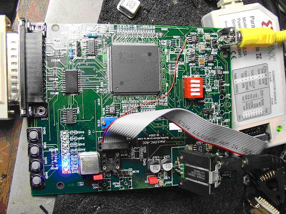
Figure 3: Photograph of the A/D converter development board.
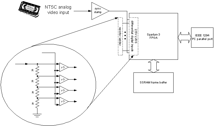
Figure 4: Basic block diagram of A/D converter board (irrelevant portions excluded).
The core Verilog code used to implement this A/D converter is given in Listing 1. The code is very simple, and it consists of just an instantiation of a set of differential input buffers and a thermometer-to-binary decoder, followed by a sampling register.
   // instantiate the LVDS input buffers
   IBUFDS_LVDSEXT_25 ibp0_p (.O(l_thermom[0]),.I(LADC_P[0]),.IB(LADC[0]));
   IBUFDS_LVDSEXT_25 ibp1_p (.O(l_thermom[1]),.I(LADC_P[1]),.IB(LADC[1]));
   IBUFDS_LVDSEXT_25 ibp2_p (.O(l_thermom[2]),.I(LADC_P[2]),.IB(LADC[2]));
   IBUFDS_LVDSEXT_25 ibp3_p (.O(l_thermom[3]),.I(LADC_P[3]),.IB(LADC[3]));
   IBUFDS_LVDSEXT_25 ibp4_p (.O(l_thermom[4]),.I(LADC_P[4]),.IB(LADC[4]));
   IBUFDS_LVDSEXT_25 ibp5_p (.O(l_thermom[5]),.I(LADC_P[5]),.IB(LADC[5]));
   IBUFDS_LVDSEXT_25 ibp6_p (.O(l_thermom[6]),.I(LADC_P[6]),.IB(LADC[6]));
   IBUFDS_LVDSEXT_25 ibp7_p (.O(l_thermom[7]),.I(LADC_P[7]),.IB(LADC[7]));
   IBUFDS_LVDSEXT_25 ibp8_p (.O(l_thermom[8]),.I(LADC_P[8]),.IB(LADC[8]));
   IBUFDS_LVDSEXT_25 ibp9_p (.O(l_thermom[9]),.I(LADC_P[9]),.IB(LADC[9]));
   IBUFDS_LVDSEXT_25 ibpa_p (.O(l_thermom[10]),.I(LADC_P[10]),.IB(LADC[10]));
   IBUFDS_LVDSEXT_25 ibpb_p (.O(l_thermom[11]),.I(LADC_P[11]),.IB(LADC[11]));
   IBUFDS_LVDSEXT_25 ibpc_p (.O(l_thermom[12]),.I(LADC_P[12]),.IB(LADC[12]));
   IBUFDS_LVDSEXT_25 ibpd_p (.O(l_thermom[13]),.I(LADC_P[13]),.IB(LADC[13]));
   IBUFDS_LVDSEXT_25 ibpe_p (.O(l_thermom[14]),.I(LADC_P[14]),.IB(LADC[14]));
   IBUFDS_LVDSEXT_25 ibpf_p (.O(l_thermom[15]),.I(LADC_P[15]),.IB(LADC[15]));

   always @(l_thermom) begin
      case(l_thermom)
	 16'b0000000000000000:	   l_binary < = 4'b0000;
	 16'b0000000000000001:	   l_binary <= 4'b0001;
	 16'b0000000000000011:	   l_binary <= 4'b0010;
	 16'b0000000000000111:	   l_binary <= 4'b0011;
	 16'b0000000000001111:	   l_binary <= 4'b0100;
	 16'b0000000000011111:	   l_binary <= 4'b0101;
	 16'b0000000000111111:	   l_binary <= 4'b0110;
	 16'b0000000001111111:	   l_binary <= 4'b0111;
	 16'b0000000011111111:	   l_binary <= 4'b1000;
	 16'b0000000111111111:	   l_binary <= 4'b1001;
	 16'b0000001111111111:	   l_binary <= 4'b1010;
	 16'b0000011111111111:	   l_binary <= 4'b1011;
	 16'b0000111111111111:	   l_binary <= 4'b1100;
	 16'b0001111111111111:	   l_binary <= 4'b1101;
	 16'b0011111111111111:	   l_binary <= 4'b1110;
	 16'b0111111111111111:	   l_binary <= 4'b1111;
	 16'b1111111111111111:	   l_binary <= 4'b1111;
	 default: l_binary <= 4'b0000;
      endcase // case(l_thermom)
   end // always @ (l_thermom)

   always @(posedge ADC_CLK) begin
      l_samp <= l_binary;
   end
Listing 1: Verilog code that forms the core of the 4-bit ADC. IBUFDS_LVDSEXT_25 is the Xilinx-specific Verilog module that creates a 2.5V LVDS input comparator. LADC and LADC_P are the analog input and the reference voltage ladder input to the Flash ADC.
Figure 5 illustrates a simple video capture taken with the 4-bit ADC clocked at 25.5454 MHz. Note that the ADC seems to have the ability to operate even faster than these rates, thus making oversampling techniques or HD-quality input possible. The video source is the NTSC output of my Sony digital still camera, so there are some screen artifacts due to icons overlayed by the camera itself. The video is not de-interlaced, so only a single field of data is shown (NTSC paints half a frame at a time, skipping every other line, so a straight time series capture of a video stream will consist of a set of half-frames (called fields) in a row). Also, no chroma (color) information is decoded, since I am just taking straight samples of data. Finally, one can see a bit of line ripple toward the edges of the video, evidence of a need for a superior “genlock” (sampling synchronization to source camera line rate) method. Despite the crudeness of this setup, a recognizable video image can be captured. The good news is that most of the issues named here are not directly a fault of the A/D converter, but rather post-processing steps specifically required to interpret digitized NTSC data.

Figure 5: Blah! what an ugly mug! Example video field capture using the basic 4-bit ADC clocked at 25.5454 MHz. The dark bars to the left and bottom are the horizontal and vertical video synchronization signals embedded in the NTSC signal stream. The picture quality isn't great, but it's a good starting point for relatively little effort. Oh, and that mess you see in the background--it's not because of the video, its because my lab is a MESS! ;-)
Interestingly, as FPGAs continue to improve in performance, hacks such as the 4-bit ADC presented in this post become easier to implement and can achieve a higher potential quality. This is due in part to improvements in the I/O comparator that is being used as the heart of the AD converter, and also due in part to improvements in the capabilities of the digital logic behind the AD converter that can be used to filter and enhance the sampled data.
Hi! I just found your website: HackDAC Implementation bunnie's blog when I was surfing around digg.com. It looks as though someone liked your website so much they decided to bookmark it. I’ll definitely be coming here more often.
Great text
Because the admin of this site is working, no uncertainty very
shortly it will be renowned, due to its quality
contents.
Hi colleagues, its wonderful piece of writing about teachingand
entirely defined, keep it up all the time.
Hi Bunnie,
thanks for this insight – any idea what signal levels can be adequately captured using the differential inputs? (searching Google I see that the NTSC votlages are between 700mV and approx 1V). I’m asking because I’m interested in capturing fast photodiode outputs, hopefully using a resistor to convert output to volts rather than needing costly highspeed transimpedance amplifiers – would a range of 1-15 mV or so be achievable do you think (ie 0 for no voltage, 8 for 8mV etc)?
[…] HackDAC Implementation […]