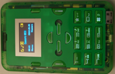
About a year and a half ago, I wrote about a $12 “Gongkai” cell phone (pictured above) that I stumbled across in the markets of Shenzhen, China. My most striking impression was that Chinese entrepreneurs had relatively unfettered access to cutting-edge technology, enabling start-ups to innovate while bootstrapping. Meanwhile, Western entrepreneurs often find themselves trapped in a spiderweb of IP frameworks, spending more money on lawyers than on tooling. Further investigation taught me that the Chinese have a parallel system of traditions and ethics around sharing IP, which lead me to coin the term “gongkai”. This is deliberately not the Chinese word for “Open Source”, because that word (kaiyuan) refers to openness in a Western-style IP framework, which this not. Gongkai is more a reference to the fact that copyrighted documents, sometimes labeled “confidential” and “proprietary”, are made known to the public and shared overtly, but not necessarily according to the letter of the law. However, this copying isn’t a one-way flow of value, as it would be in the case of copied movies or music. Rather, these documents are the knowledge base needed to build a phone using the copyright owner’s chips, and as such, this sharing of documents helps to promote the sales of their chips. There is ultimately, if you will, a quid-pro-quo between the copyright holders and the copiers.

This fuzzy, gray relationship between companies and entrepreneurs is just one manifestation of a much broader cultural gap between the East and the West. The West has a “broadcast” view of IP and ownership: good ideas and innovation are credited to a clearly specified set of authors or inventors, and society pays them a royalty for their initiative and good works. China has a “network” view of IP and ownership: the far-sight necessary to create good ideas and innovations is attained by standing on the shoulders of others, and as such there is a network of people who trade these ideas as favors among each other. In a system with such a loose attitude toward IP, sharing with the network is necessary as tomorrow it could be your friend standing on your shoulders, and you’ll be looking to them for favors. This is unlike the West, where rule of law enables IP to be amassed over a long period of time, creating impenetrable monopoly positions. It’s good for the guys on top, but tough for the upstarts.
This brings us to the situation we have today: Apple and Google are building amazing phones of outstanding quality, and start-ups can only hope to build an appcessory for their ecosystem. I’ve reviewed business plans of over a hundred hardware startups by now, and most of them are using overpriced chipsets built using antiquated process technologies as their foundation. I’m no exception to this rule – we use the Freescale i.MX6 for Novena, which is neither the cheapest nor the fastest chip on the market, but it is the one chip where anyone can freely download almost complete documentation and anyone can buy it on Digikey. This parallel constraint of scarce documentation and scarce supply for cutting edge technology forces Western hardware entrepreneurs to look primarily at Arduino, Beaglebone and Raspberry Pi as starting points for their good ideas.

Above: Every object pictured is a phone. Inset: detail of the “Skeleton” novelty phone. Image credits: Halfdan, Rachel Kalmar
Chinese entrepreneurs, on the other hand, churn out new phones at an almost alarming pace. Phone models change on a seasonal basis. Entrepreneurs experiment all the time, integrating whacky features into phones, such as cigarette lighters, extra-large battery packs (that can be used to charge another phone), huge buttons (for the visually impaired), reduced buttons (to give to children as emergency-call phones), watch form factors, and so forth. This is enabled because very small teams of engineers can obtain complete design packages for working phones – case, board, and firmware – allowing them to fork the design and focus only on the pieces they really care about.
As a hardware engineer, I want that. I want to be able to fork existing cell phone designs. I want to be able to use a 364 MHz 32-bit microcontroller with megabytes of integrated RAM and dozens of peripherals costing $3 in single quantities, instead of a 16 MHz 8-bit microcontroller with a few kilobytes of RAM and a smattering of peripherals costing $6 in single quantities. Unfortunately, queries into getting a Western-licensed EDK for the chips used in the Chinese phones were met with a cold shoulder – our volumes are too small, or we have to enter minimum purchase agreements backed by hundreds of thousands of dollars in a cash deposit; and even then, these EDKs don’t include all the reference material the Chinese get to play with. The datasheets are incomplete and as a result you’re forced to use their proprietary OS ports. It feels like a case of the nice guys finishing last. Can we find a way to still get ahead, yet still play nice?
We did some research into the legal frameworks and challenges around absorbing Gongkai IP into the Western ecosystem, and we believe we’ve found a path to repatriate some of the IP from Gongkai into proper Open Source. However, I must interject with a standard disclaimer: we’re not lawyers, so we’ll tell you our beliefs but don’t construe them as legal advice. Our intention is to exercise our right to reverse engineer in a careful, educated fashion to increase the likelihood that, if push comes to shove, the courts will agree with our actions. However, we also feel that shying away from reverse engineering simply because it’s controversial is a slippery slope: you must exercise your rights to have them. If women didn’t vote and black people sat in the back of the bus because they were afraid of controversy, the US would still be segregated and without universal suffrage.
Sometimes, you just have to stand up and assert your rights.
There are two broad categories of issues we have to deal with, patents and copyrights. For patents, the issues are complex, yet it seems the most practical approach is to essentially punt on the issue. This is what the majority of the open source community does, and in fact many corporations have similar policies at the engineering level. Nobody, as far as we know, checks their Linux commits for patent infringement before upstreaming them. Why? Among other reasons, it takes a huge amount of resources to determine which patents apply, and if one could be infringing; and even after expending those resources, one cannot be 100% sure. Furthermore, if one becomes very familiar with the body of patents, it amplifies the possibility that an infringement, should it be found, is willful and thus triple damages. Finally, it’s not even clear where the liability lies, particularly in an open source context. Thus, we do our best not to infringe, but cannot be 100% sure that no one will allege infringement. However, we do apply a license to our work which has a “poison pill” clause for patent holders that do attempt to litigate.
For copyrights, the issue is also extremely complex. The EFF’s Coders’ Rights Project has a Reverse Engineering FAQ that’s a good read if you really want to dig into the issues. The tl;dr is that courts have found that reverse engineering to understand the ideas embedded in code and to achieve interoperability is fair use. As a result, we have the right to study the Gongkai-style IP, understand it, and produce a new work to which we can apply a Western-style Open IP license. Also, none of the files or binaries were encrypted or had access controlled by any technological measure – no circumvention, no DMCA problem.
Furthermore, all the files were obtained from searches linking to public servers – so no CFAA problem, and none of the devices we used in the work came with shrink-wraps, click-throughs, or other end-user license agreements, terms of use, or other agreements that could waive our rights.
Thus empowered by our fair use rights, we decided to embark on a journey to reverse engineer the Mediatek MT6260. It’s a 364 MHz, ARM7EJ-S, backed by 8MiB of RAM and dozens of peripherals, from the routine I2C, SPI, PWM and UART to tantalizing extras like an LCD + touchscreen controller, audio codec with speaker amplifier, battery charger, USB, Bluetooth, and of course, GSM. The gray market prices it around $3/unit in single quantities. You do have to read or speak Chinese to get it, and supply has been a bit spotty lately due to high Q4 demand, but we’re hoping the market will open up a bit as things slow down for Chinese New Year.
For a chip of such complexity, we don’t expect our two-man team to be able to unravel its entirety working on it as a part-time hobby project over the period of a year. Rather, we’d be happy if we got enough functionality so that the next time we reach for an ATMega or STM32, we’d also seriously consider the MT6260 as an alternative. Thus, we set out as our goal to port NuttX, a BSD-licensed RTOS, to the chip, and to create a solid framework for incrementally porting drivers for the various peripherals into NuttX. Accompanying this code base would be original hardware schematics, libraries and board layouts that are licensed using CC BY-SA-3.0 plus an Apache 2.0 rider for patent issues.
And thus, the Fernvale project was born.
Fernvale Hardware
Compared to the firmware, the hardware reverse engineering task was fairly straightforward. The documents we could scavenge gave us a notion of the ball-out for the chip, and the naming scheme for the pins was sufficiently descriptive that I could apply common sense and experience to guess the correct method for connecting the chip. For areas that were ambiguous, we had some stripped down phones I could buzz out with a multimeter or stare at under a microscope to determine connectivity; and in the worst case I could also probe a live phone with an oscilloscope just to make sure my understanding was correct.
The more difficult question was how to architect the hardware. We weren’t gunning to build a phone – rather, we wanted to build something a bit closer to the Spark Core, a generic SoM that can be used in various IoT-type applications. In fact, our original renderings and pin-outs were designed to be compatible with the Spark ecosystem of hardware extensions, until we realized there were just too many interesting peripherals in the MT6260 to fit into such a small footprint.


Above: early sketches of the Fernvale hardware
We settled eventually upon a single-sided core PCB that we call the “Fernvale Frond” which embeds the microUSB, microSD, battery, camera, speaker, and Bluetooth functionality (as well as the obligatory buttons and LED). It’s slim, at 3.5mm thick, and at 57x35mm it’s also on the small side. We included holes to mount a partial set of pin headers, spaced to be compatible with an Arduino, although it can only be plugged into 3.3V-compatible Arduino devices.
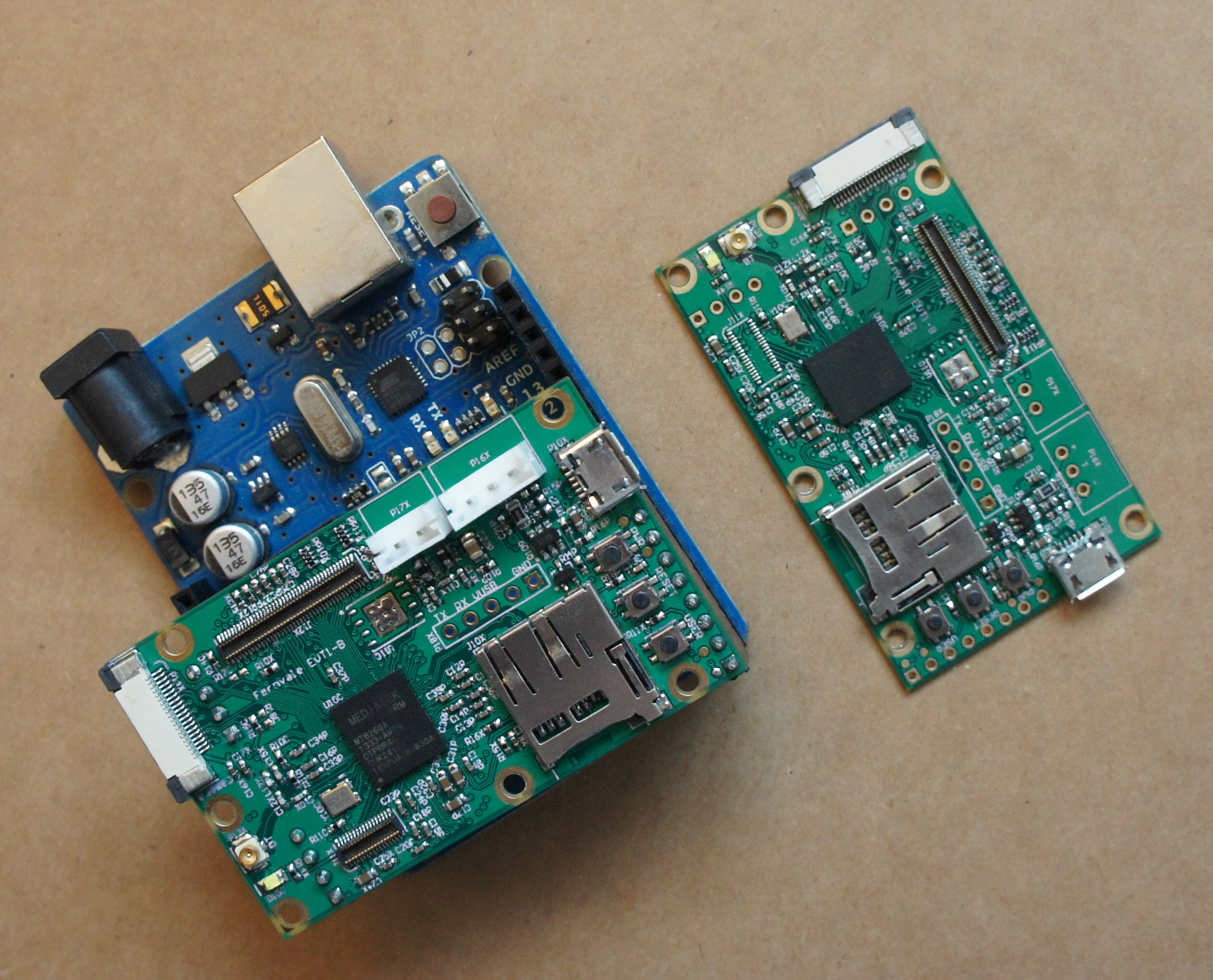
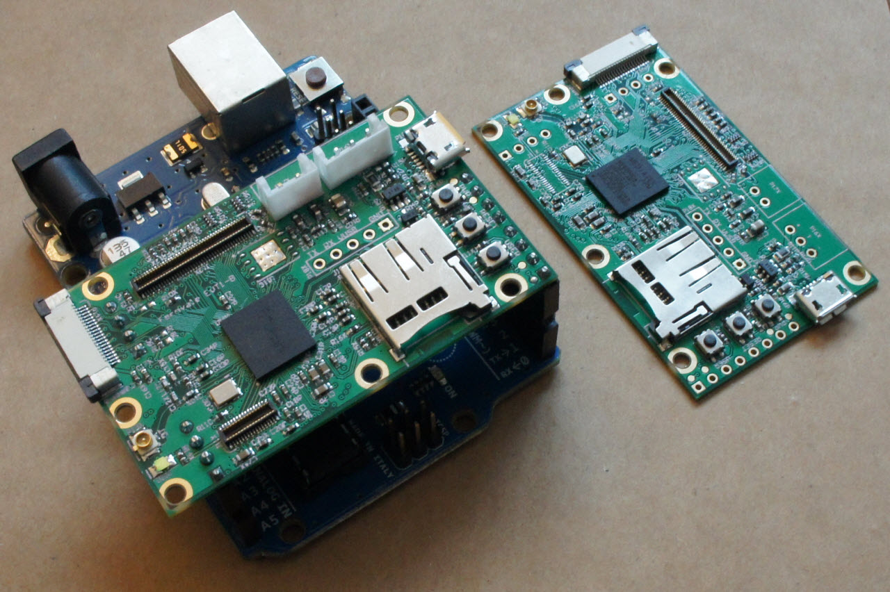
Above: actual implementation of Fernvale, pictured with Arduino for size reference
The remaining peripherals are broken out to a pair of connectors. One connector is dedicated to GSM-related signals; the other to UI-related peripherals. Splitting GSM into a module with many choices for the RF front end is important, because it makes GSM a bona-fide user-installed feature, thus pushing the regulatory and emissions issue down to the user level. Also, splitting the UI-related features out to another board costs down the core module, so it can fit into numerous scenarios without locking users into a particular LCD or button arrangement.
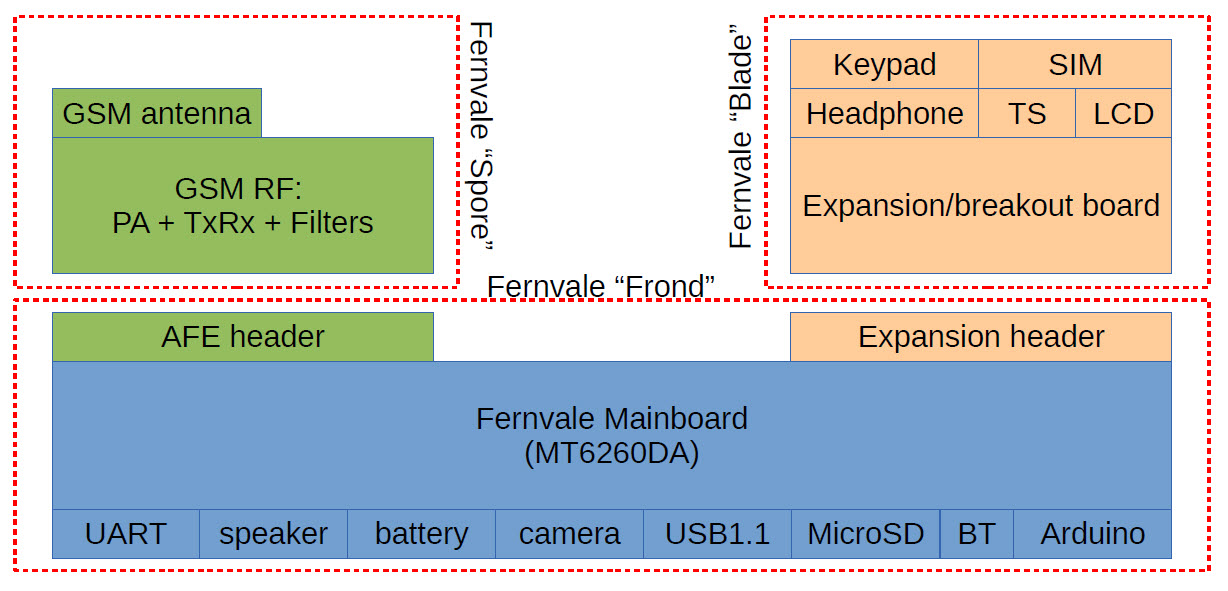
Above: Fernvale system diagram, showing the features of each of the three boards
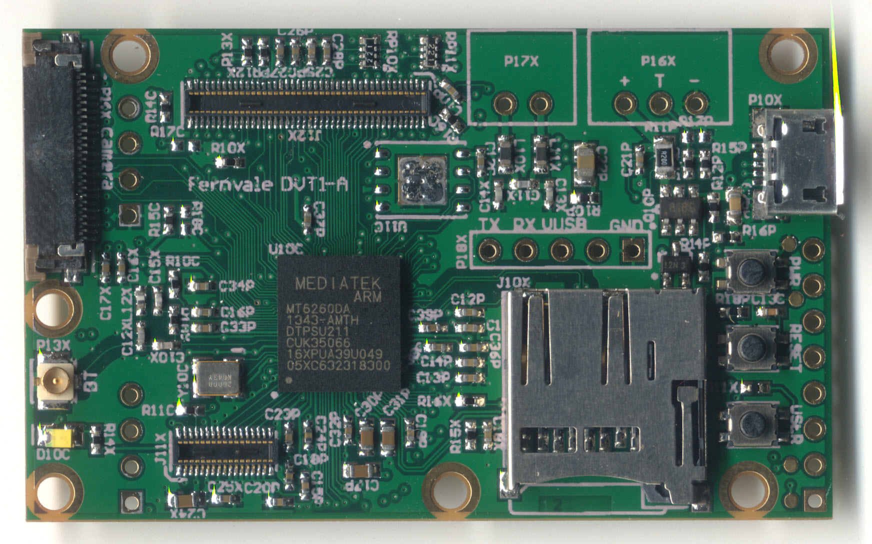
Fernvale Frond mainboard
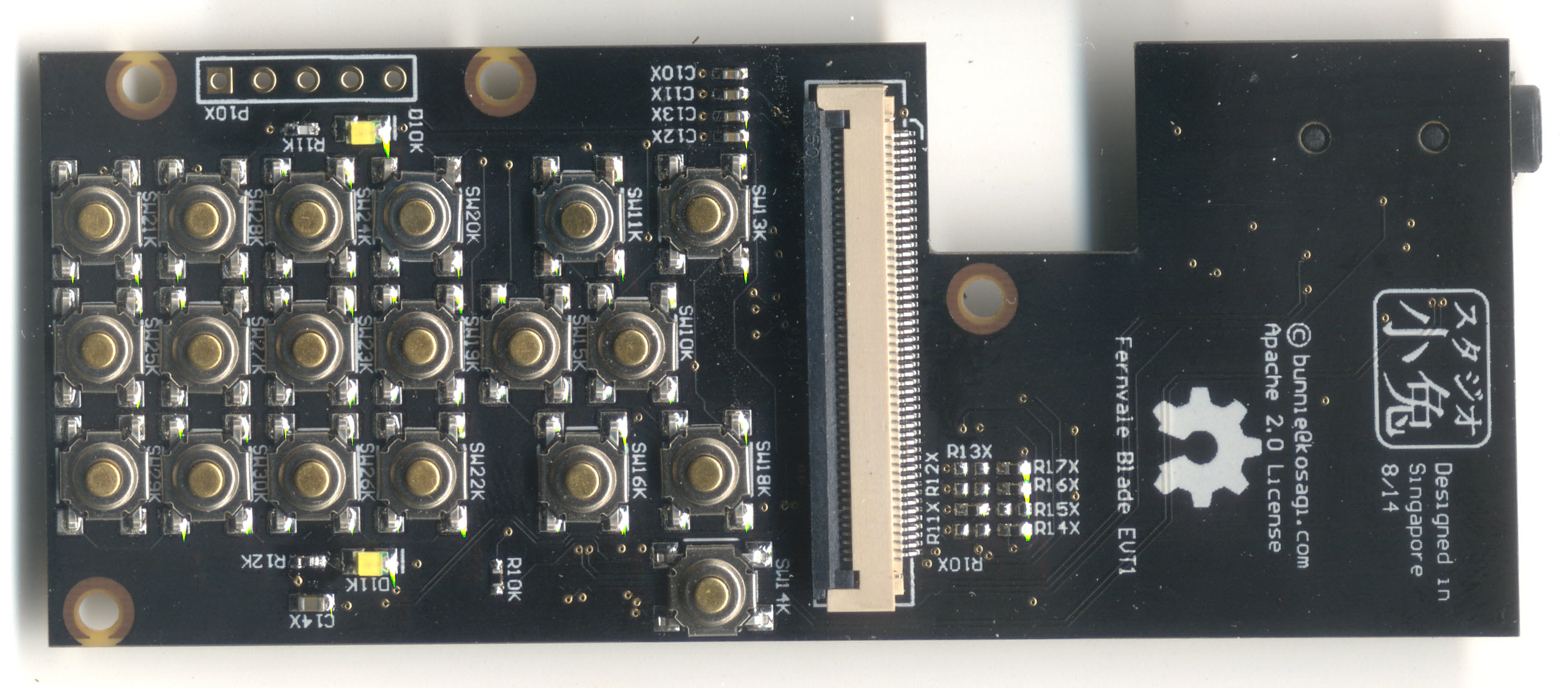
Fernvale blade UI breakout
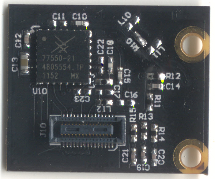
Fernvale spore AFE dev board
All the hardware source documents can be downloaded from our wiki.
As an interesting side-note, I had some X-rays taken of the MT6260. We did this to help us identify fake components, just in case we encountered units being sold as empty epoxy blocks, or as remarked versions of other chips (the MT6260 has variants, such as the -DA and the -A, the difference being how much on-chip FLASH is included).
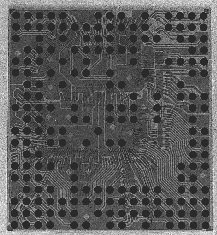
X-ray of the MT6260 chip. A sharp eye can pick out the outline of multiple ICs among the wirebonds. Image credit: Nadya Peek
To our surprise, this $3 chip didn’t contain a single IC, but rather, it’s a set of at least 4 chips, possibly 5, integrated into a single multi-chip module (MCM) containing hundreds of wire bonds. I remember back when the Pentium Pro’s dual-die package came out. That sparked arguments over yielded costs of MCMs versus using a single bigger die; generally, multi-chip modules were considered exotic and expensive. I also remember at the time, Krste Asanović, then a professor at the MIT AI Lab now at Berkeley, told me that the future wouldn’t be system on a chip, but rather “system mostly on a chip”. The root of his claim is that the economics of adding in mask layers to merge DRAM, FLASH, Analog, RF, and Digital into a single process wasn’t favorable, and instead it would be cheaper and easier to bond multiple die together into a single package. It’s a race between the yield and cost impact (both per-unit and NRE) of adding more process steps in the semiconductor fab, vs. the yield impact (and relative reworkability and lower NRE cost) of assembling modules. Single-chip SoCs was the zeitgeist at the time (and still kind of is), so it’s interesting to see a significant datapoint validating Krste’s insight.
Reversing the Boot Structure
The amount of documentation made available to Shanzhai engineers in China seems to be just enough to enable them to assemble a phone and customize its UI, but not enough to do a full OS port. You eventually come to recognize that all the phones based on a particular chipset have the same backdoor codes, and often times the UI is inconsistent with the implemented hardware. For example, the $12 phone mentioned at the top of the post will prompt you to plug headphones into the headphone jack for the FM radio to work, yet there is no headphone jack provided in the hardware. In order to make Fernvale accessible to engineers in the West, we had to reconstruct everything from scratch, from the toolchain, to the firmware flashing tool, to the OS, to the applications. Given that all the Chinese phone implementations simply rely upon Mediatek’s proprietary toolchain, we had to do some reverse engineering work to figure out the boot process and firmware upload protocol.
My first step is always to dump the ROM, if possible. We found exactly one phone model which featured an external ROM that we could desolder (it uses the -D ROMless variant of the chip), and we read its contents using a conventional ROM reader. The good news is that we saw very little ciphertext in the ROM; the bad news is there’s a lot of compressed data. Below is a page from our notes after doing a static analysis on the ROM image.
0x0000_0000		media signature “SF_BOOT”
0x0000_0200		bootloader signature “BRLYT”, “BBBB”
0x0000_0800		sector header 1 (“MMM.8”)
0x0000_09BC		reset vector table
0x0000_0A10		start of ARM32 instructions – stage 1 bootloader?
0x0000_3400		sector header 2 (“MMM.8”) – stage 2 bootloader?
0x0000_A518		thunk table of some type
0x0000_B704		end of code (padding until next sector)
0x0001_0000		sector header 3( “MMM.8”) – kernel?
0x0001_0368		jump table + runtime setup (stack, etc.)
0x0001_0828		ARM thumb code start – possibly also baseband code
0x0007_2F04		code end
0x0007_2F05 – 0x0009_F0005	padding “DFFF”
0x0009_F006		code section begin “Accelerated Technology / ATI / Nucleus PLUS”
0x000A_2C1A		code section end; pad with zeros
0x000A_328C		region of compressed/unknown data begin
0x007E_E200		modified FAT partition #1
0x007E_F400		modified FAT partition #2
One concern about reverse engineering SoCs is that they have an internal boot ROM that is always run before code is loaded from an external device. This internal ROM can also have signature and security checks that prevent tampering with the external code, and so to determine the effort level required we wanted to quickly figure out how much code was running inside the CPU before jumping to external boot code. This task was made super-quick, done in a couple hours, using a Tek MDO4104B-6. It has the uncanny ability to take deep, high-resolution analog traces and do post-capture analysis as digital data. For example, we could simply probe around while cycling power until we saw something that looked like RS-232, and then run a post-capture analysis to extract any ASCII text that could be coded in the analog traces. Likewise, we could capture SPI traces and the oscilloscope could extract ROM access patterns through a similar method. By looking at the timing of text emissions versus SPI ROM address patterns, we were able to quickly determine that if the internal boot ROM did any verification, it was minimal and nothing approaching the computational complexity of RSA.

Above: Screenshot from the Tek MDO4104B-6, showing the analog trace in yellow, and the ASCII data extracted in cyan. The top quarter shows a zoomed-out view of the entire capture; one can clearly see how SPI ROM accesses in gray are punctuated with console output in cyan.
From here, we needed to speed up our measure-modify-test loop; desoldering the ROM, sticking it in a burner, and resoldering it onto the board was going to get old really fast. Given that we had previously implemented a NAND FLASH ROMulator on Novena, it made sense to re-use that code base and implement a SPI ROMulator. We hacked up a GPBB board and its corresponding FPGA code, and implemented the ability to swap between the original boot SPI ROM and a dual-ported 64kiB emulator region that is also memory-mapped into the Novena Linux host’s address space.

Block diagram of the SPI ROMulator FPGA
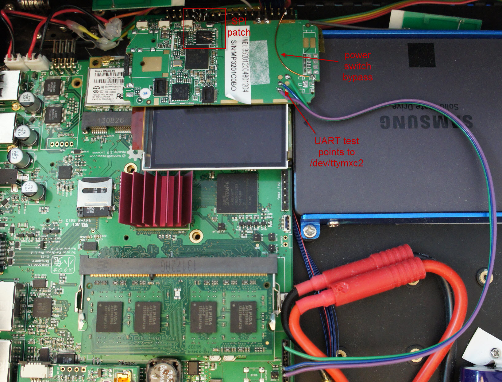
There’s a phone in my Novena! What’s that doing there?
A combination of these tools – the address stream determined by the Tek oscilloscope, rapid ROM patching by the ROMulator, and static code analysis using IDA (we found a SHA-1 implementation) – enabled us to determine that the initial bootloader, which we refer to as the 1bl, was hash-checked using a SHA-1 appendix.
Building a Beachhead
The next step was to create a small interactive shell which we could use as a beachhead for running experiments on the target hardware. Xobs created a compact REPL environment called Fernly which supports commands like peeking and poking to memory, and dumping CPU registers.
Because we designed the ROMulator to make the emulated ROM appear as a 64k memory-mapped window on a Linux host, it enables the use a variety of POSIX abstractions, such as mmap(), open() (via /dev/mem), read() and write(), to access the emulated ROM. xobs used these abstractions to create an I/O target for radare2. The I/O target automatically updates the SHA-1 hash every time we made changes in the 1bl code space, enabling us to do cute things like interactively patch and disassemble code within the emulated ROM space.

We also wired up the power switch of the phone to an FPGA I/O, so we could write automated scripts that toggle the power on the phone while updating the ROM contents, allowing us to do automated fuzzing of unknown hardware blocks.
Attaching a Debugger
Because of the difficulty in trying to locate critical blocks, and because JTAG is multiplexed with critical functions on the target device, an unconventional approach was taken to attach a debugger: xobs emulates the ARM core, and uses his fernly shell to reflect virtual loads and stores to the live target. This allows us to attach a remote debugger to the emulated core, bypassing the need for JTAG and allowing us to use cross-platform tools such as IDA on x86 for the reversing UI.
At the heart of this technique is Qemu, a multi-platform system emulator. It supports emulating ARM targets, specifically the ARMv5 used in the target device. A new machine type was created called “fernvale” that implements part of the observed hardware on the target, and simply passes unknown memory accesses directly to the device.
The Fernly shell was stripped down to only support three commands: write, read, and zero-memory. The write command pokes a byte, word, or dword into RAM on the live target, and a read command reads a byte, word, or dword from the live target. The zero-memory command is an optimization, as the operating system writes large quantities of zeroes across a large memory area.
In addition, the serial port registers are hooked and emulated, allowing a host system to display serial data as if it were printed on the target device. Finally, SPI, IRAM, and PSRAM are all emulated as they would appear on the real device. Other areas of memory are either trapped and funneled to the actual device, or are left unmapped and are reported as errors by Qemu.
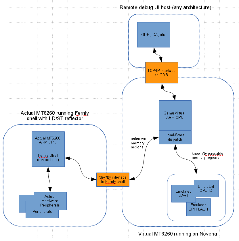
The diagram above illustrates the architecture of the debugger.
Invoking the debugger is a multi-stage process. First, the actual MT6260 target is primed with the Fernly shell environment. Then, the Qemu virtual ARM CPU is “booted” using the original vendor image – or rather, primed with a known register state at a convenient point in the boot process. At this point, code execution proceeds on the virtual machine until a load or store is performed to an unknown address. Virtual machine execution is paused while a query is sent to the real MT6260 via the Fernly shell interface, and the load or store is executed on the real machine. The results of this load or store is then relayed to the virtual machine and execution is resumed. Of course, Fernly will crash if a store happens to land somewhere inside its memory footprint. Thus, we had to hide the Fernly shell code in a region of IRAM that’s trapped and emulated, so loads and stores don’t overwrite the shell code. Running Fernly directly out of the SPI ROM also doesn’t work as part of the initialization routine of the vendor binary modifies SPI ROM timings, causing SPI emulation to fail.
Emulating the target CPU allows us to attach a remote debugger (such as IDA) via GDB over TCP without needing to bother with JTAG. The debugger has complete control over the emulated CPU, and can access its emulated RAM. Furthermore, due to the architecture of qemu, if the debugger attempts to access any memory-mapped IO that is redirected to the real target, the debugger will be able to display live values in memory. In this way, the real target hardware is mostly idle, and is left running in the Fernly shell, while the virtual CPU performs all the work. The tight integration of this package with IDA-over-GDB also allows us to very quickly and dynamically execute subroutines and functions to confirm their purpose.
Below is an example of the output of the hybrid Qemu/live-target debug harness. You can see the trapped serial writes appearing on the console, plus a log of the writes and reads executed by the emulated ARM CPU, as they are relayed to the live target running the reduced Fernly shell.
bunnie@bunnie-novena-laptop:~/code/fernvale-qemu$ ./run.sh

~~~ Welcome to MTK Bootloader V005 (since 2005) ~~~
**===================================================**

READ WORD Fernvale Live 0xa0010328 = 0x0000... ok
WRITE WORD Fernvale Live 0xa0010328 = 0x0800... ok
READ WORD Fernvale Live 0xa0010230 = 0x0001... ok
WRITE WORD Fernvale Live 0xa0010230 = 0x0001... ok
READ DWORD Fernvale Live 0xa0020c80 = 0x11111011... ok
WRITE DWORD Fernvale Live 0xa0020c80 = 0x11111011... ok
READ DWORD Fernvale Live 0xa0020c90 = 0x11111111... ok
WRITE DWORD Fernvale Live 0xa0020c90 = 0x11111111... ok
READ WORD Fernvale Live 0xa0020b10 = 0x3f34... ok
WRITE WORD Fernvale Live 0xa0020b10 = 0x3f34... ok
From this beachhead, we were able to discover the offsets of a few IP blocks that were re-used from previous known Mediatek chips (such as the MT6235 in the osmocomBB http://bb.osmocom.org/trac/wiki/MT6235) by searching for their “signature”. The signature ranged from things as simple as the power-on default register values, to changes in bit patterns due to the side effects of bit set/clear registers located at offsets within the IP block’s address space. Using this technique, we were able to find the register offsets of several peripherals.

Booting an OS
From here we were able to progress rapidly on many fronts, but our goal of a port of NuttX remained elusive because there was no documentation on the interrupt controller within the canon of Shanzhai datasheets. Although we were able to find the routines that installed the interrupt handlers through static analysis of the binaries, we were unable to determine the address offsets of the interrupt controller itself.
At this point, we had to open the Mediatek codebase and refer to the include file that contained the register offsets and bit definitions of the interrupt controller. We believe this is acceptable because facts are not copyrightable. Justice O’Connor wrote in Feist v. Rural (449 U.S. 340, 345, 349 (1991). See also Sony Computer Entm’t v. Connectix Corp., 203 F. 3d 596, 606 (9th Cir. 2000); Sega Enterprises Ltd. v. Accolade, Inc., 977 F.2d 1510, 1522-23 (9th Cir. 1992)) that
“Common sense tells us that 100 uncopyrightable facts do not magically change their status when gathered together in one place. … The key to resolving the tension lies in understanding why facts are not copyrightable: The sine qua non of copyright is originality”
and
“Notwithstanding a valid copyright, a subsequent compiler remains free to use the facts contained in another’s publication to aid in preparing a competing work, so long as the competing work does not feature the same selection and arrangement”.
And so here, we must tread carefully: we must extract facts, and express them in our own selection and arrangement. Just as the facts that “John Doe’s phone number is 555-1212” and “John Doe’s address is 10 Main St.” is not copyrightable, we need to extract facts such as “The interrupt controller’s base address in 0xA0060000”, and “Bit 1 controls status reporting of the LCD” from the include files, and re-express them in our own header files.
The situation is further complicated by blocks for which we have absolutely no documentation, not even an explanation of what the registers mean or how the blocks function. For these blocks, we reduce their initialization into a list of address and data pairs, and express this in a custom scripting language called “scriptic”. We invented our own language to avoid subconscious plagiarism – it is too easy to read one piece of code and, from memory, code something almost exactly the same. By transforming the code into a new language, we’re forced to consider the facts presented and express them in an original arrangement.
Scriptic is basically a set of assembler macros, and the syntax is very simple. Here is an example of a scriptic script:
#include "scriptic.h"
#include "fernvale-pll.h"

sc_new "set_plls", 1, 0, 0

  sc_write16 0, 0, PLL_CTRL_CON2
  sc_write16 0, 0, PLL_CTRL_CON3
  sc_write16 0, 0, PLL_CTRL_CON0
  sc_usleep 1

  sc_write16 1, 1, PLL_CTRL_UPLL_CON0
  sc_write16 0x1840, 0, PLL_CTRL_EPLL_CON0
  sc_write16 0x100, 0x100, PLL_CTRL_EPLL_CON1
  sc_write16 1, 0, PLL_CTRL_MDDS_CON0
  sc_write16 1, 1, PLL_CTRL_MPLL_CON0
  sc_usleep 1

  sc_write16 1, 0, PLL_CTRL_EDDS_CON0
  sc_write16 1, 1, PLL_CTRL_EPLL_CON0
  sc_usleep 1

  sc_write16 0x4000, 0x4000, PLL_CTRL_CLK_CONDB
  sc_usleep 1

  sc_write32 0x8048, 0, PLL_CTRL_CLK_CONDC
  /* Run the SPI clock at 104 MHz */
  sc_write32 0xd002, 0, PLL_CTRL_CLK_CONDH
  sc_write32 0xb6a0, 0, PLL_CTRL_CLK_CONDC
  sc_end
This script initializes the PLL on the MT6260. To contrast, here’s the first few lines of the code snippet from which this was derived:
// enable HW mode TOPSM control and clock CG of PLL control

*PLL_PLL_CON2 = 0x0000; // 0xA0170048, bit 12, 10 and 8 set to 0 to enable TOPSM control
                        // bit 4, 2 and 0 set to 0 to enable clock CG of PLL control
*PLL_PLL_CON3 = 0x0000; // 0xA017004C, bit 12 set to 0 to enable TOPSM control

// enable delay control
*PLL_PLLTD_CON0= 0x0000; //0x A0170700, bit 0 set to 0 to enable delay control

//wait for 3us for TOPSM and delay (HW) control signal stable
for(i = 0 ; i < loop_1us*3 ; i++);

//enable and reset UPLL
reg_val = *PLL_UPLL_CON0;
reg_val |= 0x0001;
*PLL_UPLL_CON0  = reg_val; // 0xA0170140, bit 0 set to 1 to enable UPLL and generate reset of UPLL
The original code actually goes on for pages and pages, and even this snippet is surrounded by conditional statements which we culled as they were not relevant facts to initializing the PLL correctly.
With this tool added to our armory, we were finally able to code sufficient functionality to boot NuttX on our own Fernvale hardware.
Toolchain
Requiring users to own a Novena ROMulator to hack on Fernvale isn't a scalable solution, and thus in order to round out the story, we had to create a complete developer toolchain. Fortunately, the compiler is fairly cut-and-dry – there are many compilers that support ARM as a target, including clang and gcc. However, flashing tools for the MT6260 are much more tricky, as all the existing ones that we know of are proprietary Windows programs, and Osmocom's loader doesn't support the protocol version required by the MT6260. Thus, we had to reverse engineer the Mediatek flashing protocol and write our own open-source tool.
Fortunately, a blank, unfused MT6260 shows up as /dev/ttyUSB0 when you plug it into a Linux host – in other words, it shows up as an emulated serial device over USB. This at least takes care of the lower-level details of sending and receiving bytes to the device, leaving us with the task of reverse engineering the protocol layer. xobs located the internal boot ROM of the MT6260 and performed static code analysis, which provided a lot of insight into the protocol. He also did some static analysis on Mediatek's Flashing tool and captured live traces using a USB protocol analyzer to clarify the remaining details. Below is a summary of the commands he extracted, as used in our open version of the USB flashing tool.
enum mtk_commands {
  mtk_cmd_old_write16 = 0xa1,
  mtk_cmd_old_read16 = 0xa2,
  mtk_checksum16 = 0xa4,
  mtk_remap_before_jump_to_da = 0xa7,
  mtk_jump_to_da = 0xa8,
  mtk_send_da = 0xad,
  mtk_jump_to_maui = 0xb7,
  mtk_get_version = 0xb8,
  mtk_close_usb_and_reset = 0xb9,
  mtk_cmd_new_read16 = 0xd0,
  mtk_cmd_new_read32 = 0xd1,
  mtk_cmd_new_write16 = 0xd2,
  mtk_cmd_new_write32 = 0xd4,
  // mtk_jump_to_da = 0xd5,
  mtk_jump_to_bl = 0xd6,
  mtk_get_sec_conf = 0xd8,
  mtk_send_cert = 0xe0,
  mtk_get_me = 0xe1, /* Responds with 22 bytes */
  mtk_send_auth = 0xe2,
  mtk_sla_flow = 0xe3,
  mtk_send_root_cert = 0xe5,
  mtk_do_security = 0xfe,
  mtk_firmware_version = 0xff,
};
Current Status and Summary
After about a year of on-and-off effort between work on the Novena and Chibitronics campaigns, we were able to boot a port of NuttX on the MT6260. A minimal set of hardware peripherals are currently supported; it’s enough for us to roughly reproduce the functionality of an AVR used in an Arduino-like context, but not much more. We’ve presented our results this year at 31C3 (slides).
The story takes an unexpected twist right around the time we were writing our CFP proposal for 31C3. The week before submission, we became aware that Mediatek released the LinkIT ONE, based on the MT2502A, in conjunction with Seeed Studios. The LinkIT ONE is directly aimed at providing an Internet of Things platform to entrepreneurs and individuals. It’s integrated into the Arduino framework, featuring an open API that enables the full functionality of the chip, including GSM functions. However, the core OS that boots on the MT2502A in the LinkIT ONE is still the proprietary Nucleus OS and one cannot gain direct access to the hardware; they must go through the API calls provided by the Arduino shim.
Realistically, it’s going to be a while before we can port a reasonable fraction of the MT6260’s features into the open source domain, and it’s quite possible we will never be able to do a blob-free implementation of the GSM call functions, as those are controlled by a DSP unit that’s even more obscure and undocumented. Thus, given the robust functionality of the LinkIT ONE compared to Fernvale, we’ve decided to leave it as an open question to the open source community as to whether or not there is value in continuing the effort to reverse engineer the MT6260: How important is it, in practice, to have a blob-free firmware?
Regardless of the answer, we released Fernvale because we think it’s imperative to exercise our fair use rights to reverse engineer and create interoperable, open source solutions. Rights tend to atrophy and get squeezed out by competing interests if they are not vigorously exercised; for decades engineers have sat on the sidelines and seen ever more expansive patent and copyright laws shrink their latitude to learn freely and to innovate. I am saddened that the formative tinkering I did as a child is no longer a legal option for the next generation of engineers. The rise of the Shanzhai and their amazing capabilities is a wake-up call. I see it as evidence that a permissive IP environment spurs innovation, especially at the grass-roots level. If more engineers become aware of their fair use rights, and exercise them vigorously and deliberately, perhaps this can catalyze a larger and much-needed reform of the patent and copyright system.
Want to read more? Check out xobs’ post on Fernvale. Want to get involved? Chime in at our forums. Or, watch the recording of our talk below.
Team Kosagi would like to once again extend a special thanks to .mudge for making this research possible.