Posts Tagged ‘hacking’

An Oscilloscope Module for Novena

Thursday, May 8th, 2014

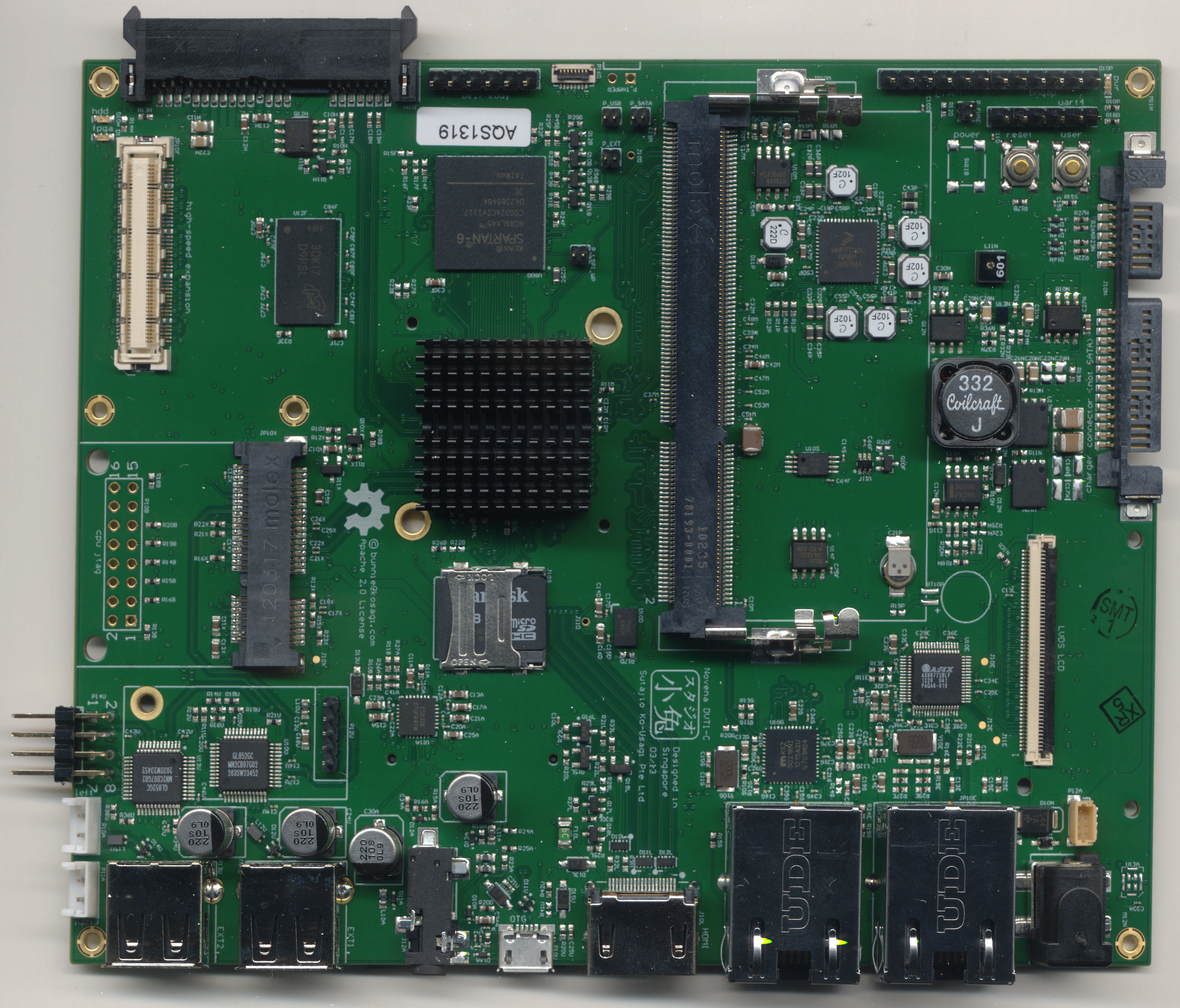
One of Novena’s most distinctive features is its FPGA co-processor. An FPGA, or Field Programmable Gate Array, is a sea of logic gates and memory elements that can be wired up according to hardware descriptions programmed in languages such as Verilog or VHDL. Verilog can be thought of as a very strictly typed C where every line of the code executes simultaneously. Thus, every bit of logic in Novena’s Spartan 6 LX45 FPGA could theoretically perform a computation every clock cycle — all 43,000 logic cells, 54,000 flip flops, and 58 fixed-point multiply accumulate DSP blocks. This potential for massive parallelism underlies one half of the exciting prospects enabled by an FPGA.

The other exciting half of an FPGA relates to its expansive I/O capabilities. Every signal pin of an FPGA can be configured to comply with a huge range of physical layer specifications, from vanilla CMOS to high-speed differential standards such as TMDS (used in HDMI) and SSTL (used to talk to DDR memories). Each signal pin is also backed by a high speed SERDES (serializer/deserializer) and sophisticated clock management technologies. Need a dozen high-precision PWM channels for robotics? No problem, an FPGA can easily do that. Need an HDMI interface or two? Also no problem. Need a bespoke 1000 MT/s ADC interface? Simple matter of programming – and all with the same set of signal pins.

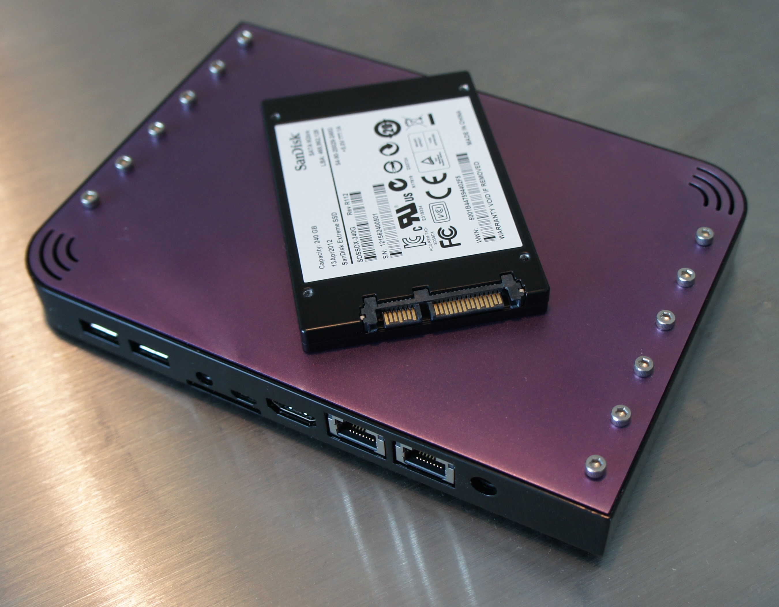
Novena also hangs a 2Gbit DDR3 memory chip directly off the FPGA. The FPGA contains a dedicated memory controller that talks DDR3 at a rate of 800MT/s over a 16-bit bus, yielding a theoretical peak memory bandwidth of 12.8 Gbits/s. This fast, deep memory is useful for caching and buffering data locally.

Thus, the FPGA can be thought of as the ultimate hardware hacking primitive. In order to unlock the full potential of the FPGA, we decided to bring most of the spare I/Os on the chip to a high speed expansion header. The high speed header is a bit less convenient than Arduino shield connectors if all you need to do is flash an LED, but as a trade-off the header is rated for signal speeds of over a gigabit per second per pin.

However, the GPBB (General Purpose Breakout Board) featured as one of the Novena crowdfunding campaign stretch goals resolves this inconvenience by converting the high speed signal format into a much lower performance but more convenient 0.1” pin header format, suitable for most robotics and home automation projects.

Enter the Oscilloscope
A problem that xobs and I frequently encounter is the need for a highly programmable, travel-friendly oscilloscope. There’s a number of USB scope solutions that don’t quite cut it in terms of analog performance and UX, and there are no self-contained solutions we know of today that allow us to craft stimulus-response loops of the type needed for fuzzing, glitching, power analysis, or other similar hardware hacking techniques.

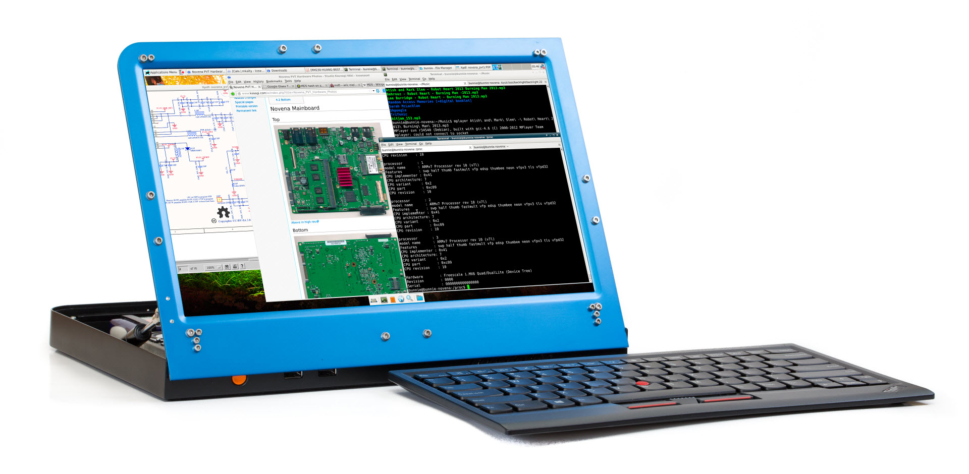
Fortunately, Novena is an ideal platform for implementing a bespoke oscilloscope solution – which we’ve gone ahead and done. Here’s a video demonstrating the basic functionality of our oscilloscope solution running on Novena (720p version in VP8 or H.264):

Novena was plugged into the large-screen TV via HDMI to make filming the video a little bit easier.

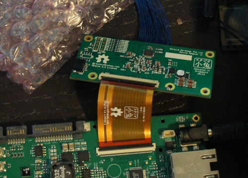
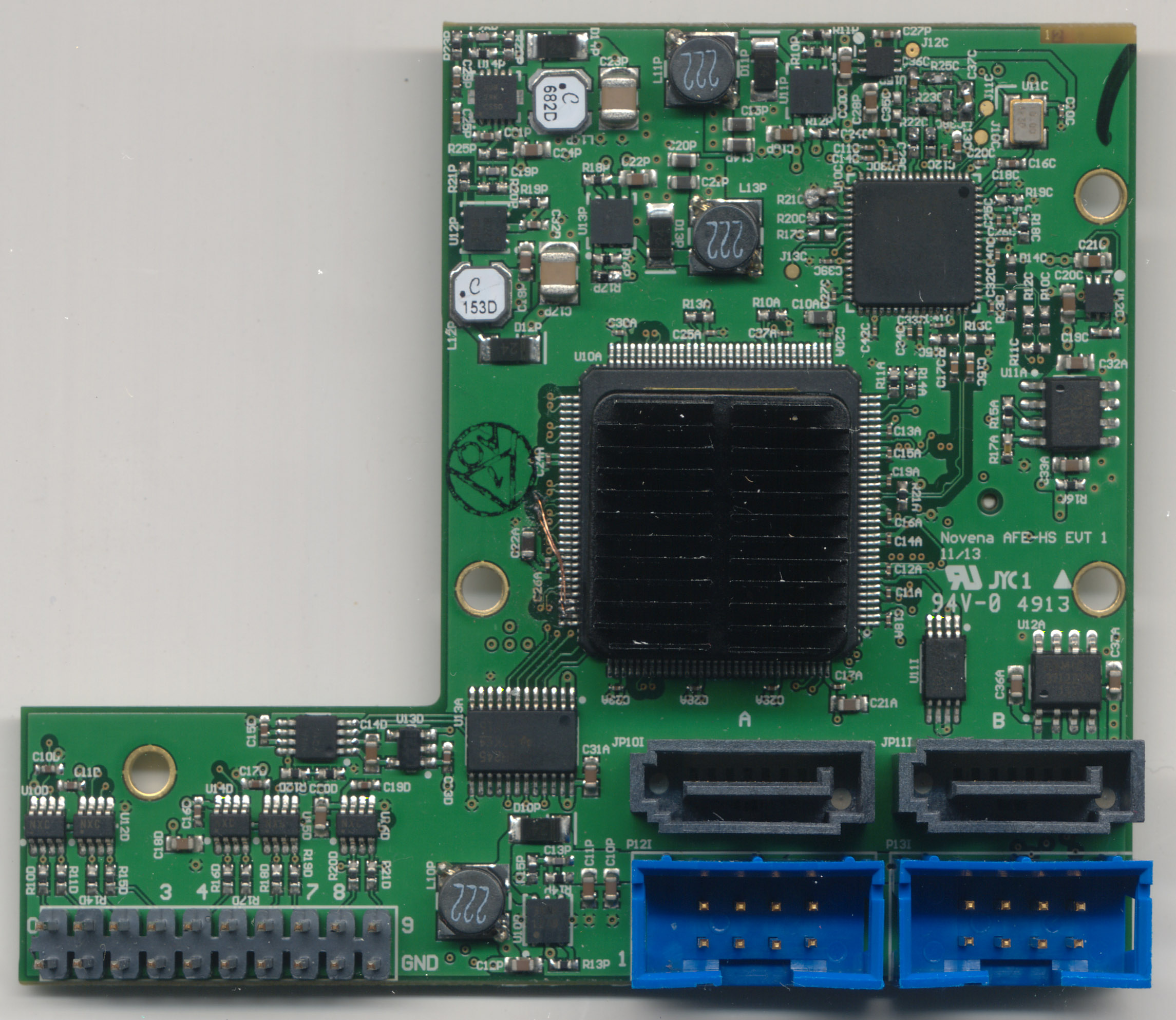
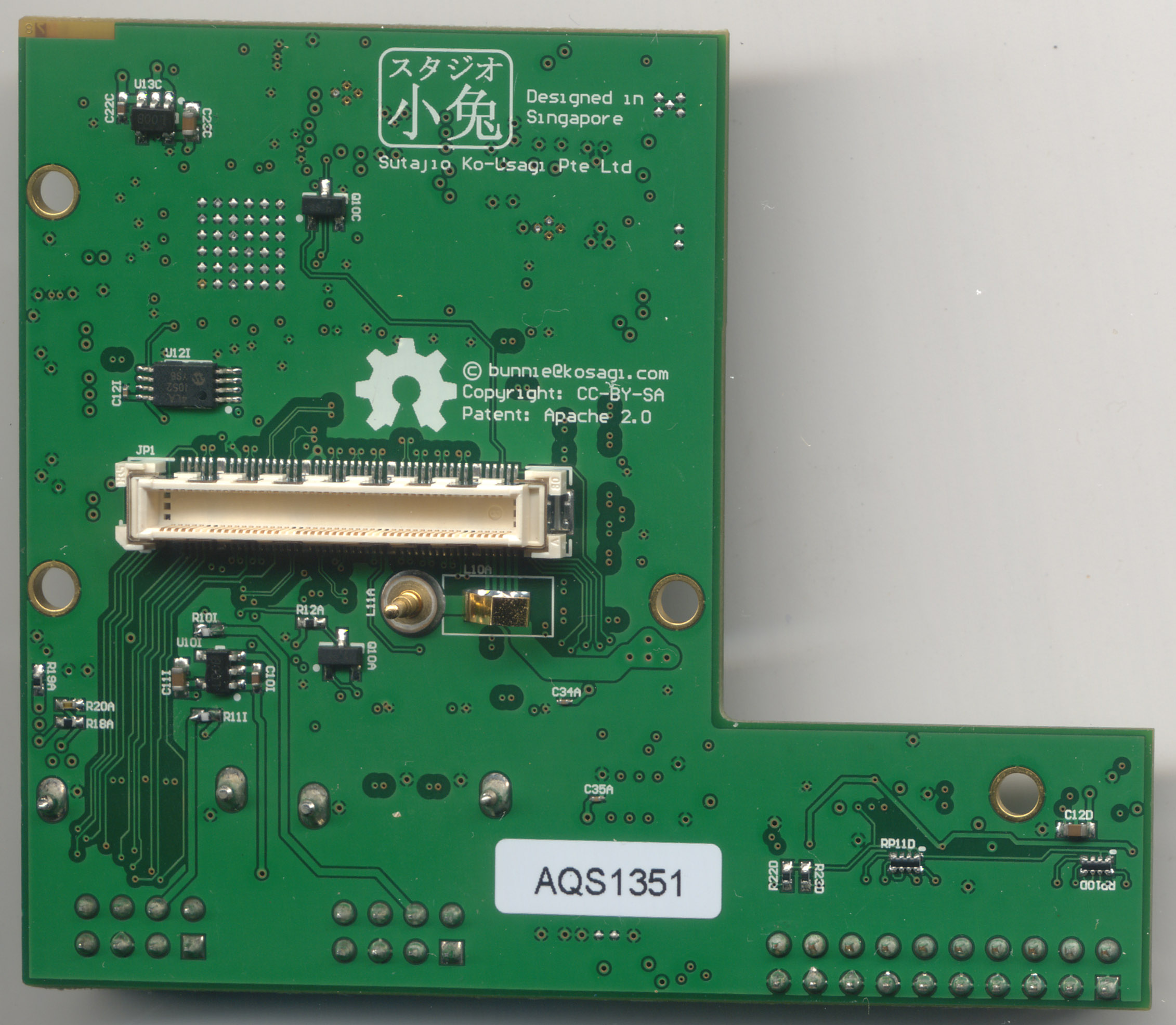
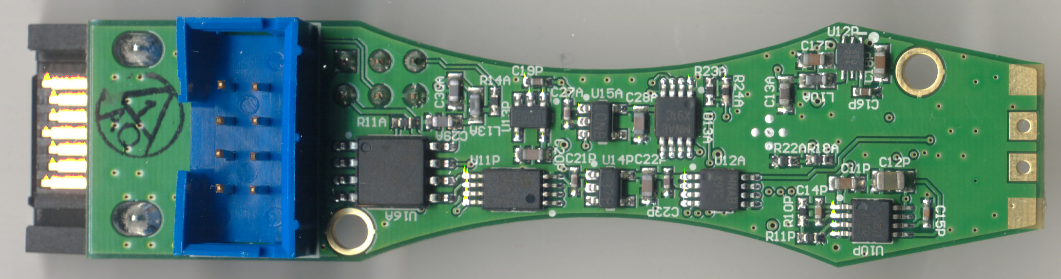
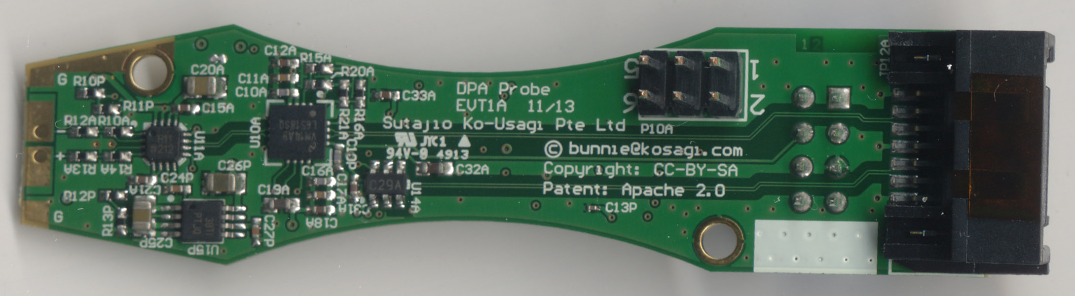
In a nutshell, the oscilloscope offers two 8-bit channels at 1GSPS or one 8-bit channel at 2GSPS with an analog bandwidth of up to 900MHz. As a side bonus we also wired in a set of 10 digital channels that can be used as a simple logic analyzer. Here’s some high resolution photos of the oscilloscope expansion board:

Here’s the schematics.

This combination of the oscilloscope expansion board plus Novena is a major step toward the realization of our dream of a programmable, travel-friendly oscilloscope. The design is still a couple revisions away from being production ready, but even in its current state it’s a useful hacking tool.

At this point, I’m going to geek out and talk about the tech behind the implementation of the oscilloscope board.

Oscilloscope Architecture
Below is a block diagram of the oscilloscope’s digital architecture.

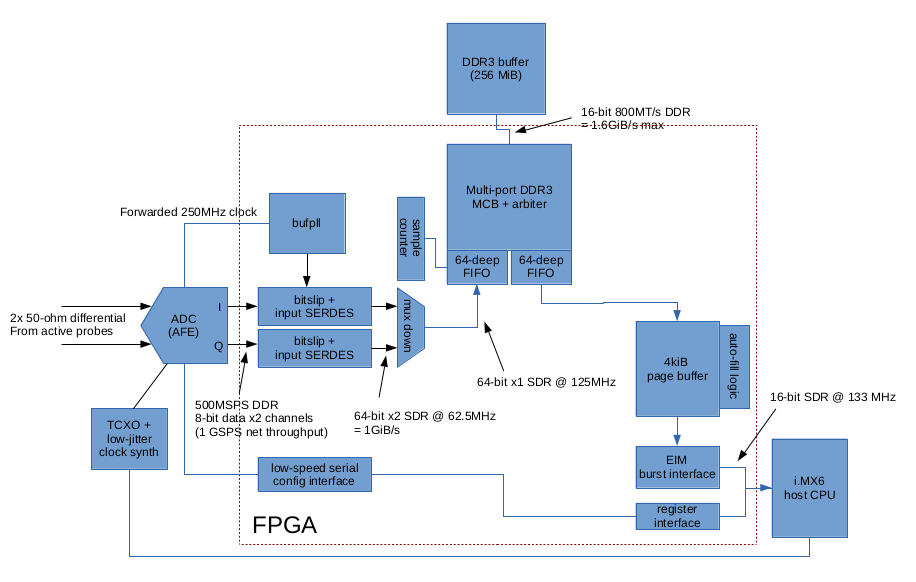
The FPGA is configured to talk to an ADC08D1020 dual 1GSPS ADC, designed originally by National Semiconductor but now sold as TI. The interface to the ADC is a pair of 8-bit differential DDR busses, operating at up to 500MHz, which is demultiplexed 1:8 into a 64-bit internal datapath. Upon receipt of a trigger condition, the FPGA stores a real-time sample data from the ADC into local DDR3 memory, and later on the CPU can stream data out of the DDR3 memory via the Linux Generic Netlink API. Because the DDR3 memory’s peak bandwidth is only 1.6GSPS, deep buffer capture of 256 Msamples is only available for net sample rates below 1GSPS; higher sample rates are limited to the internal memory capacity of the FPGA, still a very usable 200 ksamples depth. The design is written in Verilog and consumes about 15% of the FPGA, leaving plenty of space for implementing other goodies like digital filters and other signal processing.

The ADC is clocked by an Analog Devices AD9520 PLL, which derives its time base from a TCXO. This PLL + TCXO combination gives us better jitter performance than the on-chip PLL of the FPGA, and also gives us more flexibility on picking sampling rates.

The power system uses a hybrid of boost, buck, and inverting switching regulators to bring voltages to the minimum-dropout required for point-of-use LDOs to provide clean power to sensitive analog subsystems. This hybrid approach makes the power system much more complex, but helps keep the power budget manageable.

Perhaps the most unique aspect of our oscilloscope design is the partitioning of the analog signal chain. Getting a signal from the point of measurement to the ADC is a major engineering challenge. Remarkably, the same passive probe I held in the 90’s is still a standard workhorse for scopes like my Tektronix TDS5104B almost a quarter century later. This design longevity is extremely rare in the world of electronics. With a bandwidth of several hundred MHz but an impedance measured in mega-ohms and a load capacitance measured in picofarads, it makes one wonder why we even bother with 50-ohm cables when we have stuff like oscilloscope probes. There’s a lot of science behind this, and as a result well-designed passive probes, such as the Tektronix P6139B, cost hundreds of dollars.

Unfortunately, high quality scope probes are made out of unicorn hair and unobtanium as far as I’m concerned, so when thinking about our design, I had to take a clean-sheet look at the problem. I decided to look at an active probe solution, whilst throwing away any notion of backward compatibility with existing scope probes.

I started the system design by first considering the wires (you can tell I’m a student of Tom Knight – one of his signature phrases is “it’s the wires, stupid!”). I concluded the cheapest high-bandwidth commodity cable that is also rated for a high insertion count is probably the SATA cable. It consists of two differential pairs and it has to support signal bandwidths measured in GHz, yet it costs just a couple of bucks. On the downside, any practical probing solution needs to present an impedance of almost a million times greater than that required by SATA, to avoid loading down the circuitry under test. This means we have to cram a high performance amplifier into a PCB that fits in the palm of your hand. Thankfully, Moore’s Law took care of that in the intervening decades from when passive oscilloscope probes were first invented out of necessity.

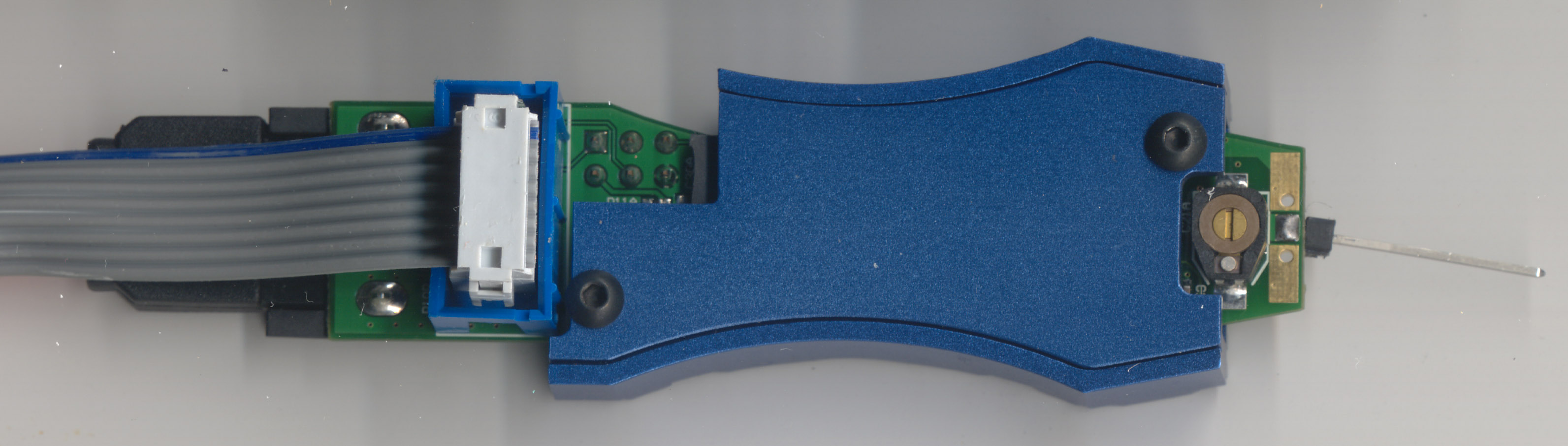
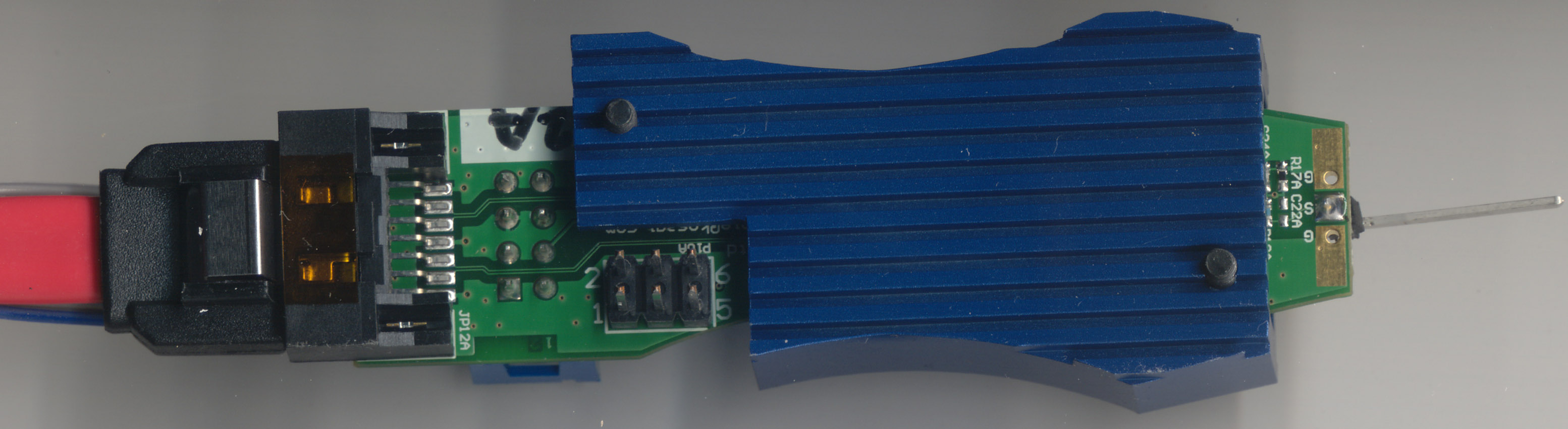
The LMH6518 is a single-chip solution for oscilloscope front-ends that is almost perfect for this scenario. It’s a 900 MHz, digitally controlled variable gain amplifier (VGA) with the added feature of an auxilliary output that’s well-suited for functioning as a trigger channel; conveniently, a SATA cable has two differential pairs, so we allocate one for measurement and one for trigger. We also strap a conventional 8-pin ribbon cable to the SATA cable for passing power and I2C.

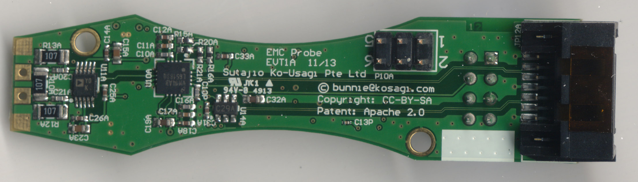
The same LMH6518 VGA can be combined with a variety of front-end amplifiers to create a range of application-specific probes. We use a 1GHz FET op-amp (the ADA4817) to do the impedance transformation required of a “standard” digital oscilloscope. We use a relatively low impedance but “true differential” amplifier to measure voltages developed across a series sense resistor for power signature analysis. And we have a very high-impedance, high CMRR instrumentation amplifier front end for capturing signals developed across small loops and stubs of wire, useful for detecting parasitic electromagnetic emissions from circuits and cables.

Above: digital probe

Above: power signature analysis probe

Above: sidechannel emissions probe

However, the design isn’t quite perfect. The LMH6518 burns a lot of power – a little over a watt; and the pre-amp plus power regulators add about another watt overall to the probe’s power footprint. Two watts isn’t that bad on an absolute scale, but two watts in the palm of your hand is searing hot; the amplifier chip gets to almost 80C. So, I designed a set of custom aluminum heatsinks for the probes to help spread and dissipate the heat.

When I handed the aluminum-cased probes to xobs, I warned him that the heat sinks are either going to solve the heat issue, or it’s going to turn the probes into a ball of flaming hot metal. Unfortunately, the heatsink gets to about 60C in still air, which is an ergonomic challenge – the threshold for pain is typically around 45-50C, so it’s very uncomfortable to hold the aluminum cases directly. It’s alright to hold the probes by the plastic connectors on the back, but this requires special training and users will instinctively want to hold a probe by its body. So, probably I’ll have to do some thermal optimization of the design and add either a heat pipe to a large heatsink off the probe body, or use a small fan to force air over the probes. It turns out just a tiny bit of airflow is all that’s need to keep the probes cool, but with passive convection alone they are simply too hot to handle. This won’t, of course, stop us from using them as-is; we’re okay with having to be a little bit careful to gain access to a very capable device. However, nanny-state laws and potentially litigious customers make it too risky to sell this solution to end consumers right now.

Firmware Architecture

xobs defined the API for the oscilloscope. The driver is based upon the Generic Netlink API native to the Linux kernel, and relies upon the libnl-genl libraries for the user-space implementation. Out of the various APIs available in the Linux kernel to couple kernelspace to userspace, Netlink was the best match, as it is stream-oriented and inherently non-blocking. This API has been optimized for high throughput and low latency, since it is also the core of the IP network stacks that on servers push gigabits of bandwidth. It’s also more mature than the nascent Linux IIO subsystem.

In the case of xobs’ driver, he creates a custom generic netlink protocol which he registers with the name “kosagi-fpga”. Generic netlink sockets support the concept of specific commands, and he currently supports the following:


/* list of valid commands */
enum kosagi_fpga_commands {
KOSAGI_CMD_UNSPEC,
KOSAGI_CMD_SEND,
KOSAGI_CMD_READ,
KOSAGI_CMD_POWER_OFF,
KOSAGI_CMD_POWER_ON,
KOSAGI_CMD_FPGA_ASSERT_RESET,
KOSAGI_CMD_FPGA_DEASSERT_RESET,
KOSAGI_CMD_TRIGGER_SAMPLE,
__KOSAGI_CMD_MAX,
};

The current implementation provisions two memory-mapped address spaces for the CPU to communicate with the FPGA, split along two different chip select lines. Chip Select 0 (CS0) is used for simple messages and register settings, while Chip Select 1 (CS1) is used for streaming data to and from the FPGA. Therefore, when the CPU wants to set capture buffer sizes, trigger conditions, or initiate a transfer, it communicates using CS0. When it wants to stream data from the FPGA, it will do so via CS1.

The core of the API is the KOSAGI_CMD_TRIGGER_SAMPLE and KOSAGI_CMD_READ commands. To request a sample from the oscilloscope, the userspace program emits a KOSAGI_CMD_TRIGGER_SAMPLE command to the kosagi-fpga Netlink interface. This will cause the CPU to communicate with the FPGA via the CS0 EIM memory space control registers, setting up the trigger condition and the transfer FIFO from the FPGA.

The userspace program will then emit a KOSAGI_CMD_READ command to retrieve the data. Upon receiving the read command, the kernel initiates a burst read from CS1 EIM memory space to a kernel buffer using memcpy(), which is forwarded back to the userspace that requested the data using the genlmsg_unicast() Netlink API call. Userspace retrieves the data stream from the kernel by calling the nl_recv() API call.

This call is currently configured to block until the data is available for the userspace program, but it can also be configured to timeout as well. However, a timeout is generally not necessary as the call will succeed in a fraction of a millisecond due to the high speed and determinism of the transfer interface.

In addition to handling data transfers, the kernel module implementing this API also handles housekeeping functions, such as configuring the FPGA and controlling power to the analog front end. FPGA configuration is handled automatically upon driver load (via insmod, modprobe, or udev) via the request_firmware() API built into the Linux kernel. The FPGA bitstream is located in the kernel firmware directory, usually /lib/firmware/novena_fpga.bit.

Power management functions have their own dedicated Netlink commands. Calling these commands causes the respective GPIO for the expansion connector power switch to be toggled. When the expanion connector is power-cycled, the module also resets the FPGA and reloads its firmware, allowing for a complete reset of the expansion subsystem without having to power cycle the CPU.

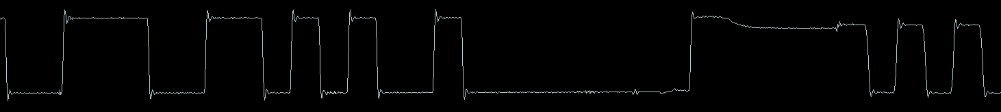
Above: a snippet of a trace captured by the scope when probing a full-speed USB data line.

xobs also wrote a wonderful demo program in Qt for the oscilloscope, and through this we were able to do some preliminary performance characterization. The rise-time performance of the probe is everything I had hoped for, and the very long capture buffer provided by the FPGA’s DDR3 memory enables a new dimension of deep signal analysis. This, backed with Novena’s horsepower, tight integration with Linux and a hackable architecture makes for a compelling – and portable – signal analysis solution for field work.

If the prospect of a a hackable oscilloscope excites you as much as it does us, please consider backing our crowdfunding campaign for Novena and spreading the word to your friends; there’s only a few days left. Developing complex hardware and software systems isn’t cheap, and your support will enable us to focus on bringing more products like this to market.

Novena’s Hackable Bezel

Saturday, May 3rd, 2014

When designing Novena, I had to balance budget against hackability. Plastic parts are cheap to produce, but the tools to mold them are very expensive and difficult to modify. Injection mold tooling cost for a conventional clamshell (two-body) laptop runs upwards of $250,000. In contrast, Novena’s single body design has a much lower tooling cost, making it feasible to amortize tooling costs over a smaller volume.

The decision to use flat sheet aluminum for the LCD bezel was also driven in part to reduce tooling costs. Production processing for aluminum can be done using CNC, virtually eliminating up-front tooling costs. Furthermore, aluminum has great hack value, as it can be cut, drilled, tapped, and bent with entry-level tools. This workability means end users can easily add connectors, buttons, sensors, and indicators to the LCD bezel. Users can even design in a custom LCD panel, since there’s almost no setup cost for machining aluminum.

One of my first mods to the bezel is a set of 3D-printed retainers, custom designed to work with my preferred keyboard. The retainers screw into a set of tapped M2.5 mounting holes around the periphery of the LCD.

The idea is that the retainers hold my keyboard against the LCD bezel when transporting the laptop, protecting the LCD from impact damage while making it a little more convenient for travel.

Such an easily customizable bezel means a limitless combination of keyboards and LCDs can be supported without requiring expensive modifications to injection molding tools.

The flat design also means it’s easy to laser-cut a bezel using other materials. Here’s an example made out of clear acrylic. The acrylic version looks quite pretty, although as a material acrylic is much softer and less durable than aluminum.

I also added a notch on the bottom part of the bezel to accommodate breakout boards plugged into the FPGA expansion connector.

The low up-front cost to modify and customize the bezel enables experimentation and serendipitous hacks. I’m looking forward to seeing what other Novena users do with their bezels!

Crowdfunding the Novena Open Laptop

Wednesday, April 2nd, 2014

We’re launching a crowdfunding campaign around our Novena open hardware computing platform. Originally, this started as a hobby project to build a computer just for me and xobs – something that we would use every day, easy to extend and to mod, our very own Swiss Army knife. I’ve posted here a couple of times about our experience building it, and it got a lot of interest. So by popular demand, we’ve prepared a crowdfunding offering and you can finally be a backer.


Background


Novena is a 1.2GHz, Freescale quad-core ARM architecture computer closely coupled with a Xilinx FPGA. It’s designed for users who want to modify and extend their hardware: all the documentation for the PCBs are open and free to download, and it comes with a variety of features that facilitate rapid prototyping.

We are offering four variations, and at the conclusion of the Crowd Supply campaign on May 18, all the prices listed below will go up by 10%:

  • “Just the board” ($500): For crafty people who want to build their case and define their own style, we’ll deliver to you the main PCBA, stuffed with 4GiB of RAM, 4GiB microSD card, and an Ath9k-based PCIe wifi card. Boots to a Debian desktop over HDMI.
  • “All-in-One Desktop” ($1195): Plug in your favorite keyboard and mouse, and you’re ready to go; perfect for labs and workbenches. You get the circuit board above, inside a hacker-friendly case with a Full HD (1920×1080) IPS LCD.
  • “Laptop” ($1995): For hackers on the go, we’ll send you the same case and board as above, but with battery controller board, 240 GiB SSD, and a user-installed battery. As everyone has their own keyboard preference, no keyboard is included.
  • “Heirloom Laptop” ($5000): A show stopper of beauty; a sure conversation piece. This will be the same board, battery, and SSD as above, but in a gorgeous, hand-crafted wood and aluminum case made by Kurt Mottweiler in Portland, Oregon. As it’s a clamshell design, it’s also the only offering that comes with a predetermined keyboard.

All configurations will come with Debian (GNU/Linux) pre-installed, but of course you can build and install whatever distro you prefer!

Novena Gen-2 Case Design

Followers of this blog may have seen a post featuring a prototype case design we put together last December. These were hand-built cases made from aluminum and leather and meant to validate the laptop use case. The design was rough and crafted by my clumsy hands – dubbed “gloriously fuggly [sic]” – yet the public response was overwhelmingly positive. It gave us confidence to proceed with a 2nd generation case design that we are now unveiling today.


The first thing you’ll notice about the design is that the screen opens “the wrong way”. This feature allows the computer to be usable as a wall-hanging unit when the screen is closed. It also solves a major problem I had with the original clamshell prototype – it was a real pain to access the hardware for hacking, as it’s blocked by the keyboard mounting plate.

Now, with the slide of a latch, the screen automatically pops open thanks to an internal gas spring. This isn’t just an open laptop — it’s a self-opening laptop! The internals are intentionally naked in this mode for easy access; it also makes it clear that this is not a computer for casual home use. Another side benefit of this design is there’s no fan noise – when the screen is up, the motherboard is exposed to open air and a passive heatsink is all you need to keep the CPU cool.

Another feature of this design is the LCD bezel is made out of a single, simple aluminum sheet. This allows users with access to a minimal machine shop to modify or craft their own bezels – no custom tooling required. Hopefully this makes adding knobs and connectors, or changing the LCD relatively easy. In order to encourage people to experiment, we will ship desktop and laptop devices with not one, but two LCD bezels, so you don’t have to worry about having an unusable machine if you mess up one of the bezels!

The panel covering the “port farm” on the right hand side of the case is designed to be replaceable. A single screw holds it in place, so if you design your own motherboard or if you want to upgrade in the future, you’re not locked into today’s port layout. We take advantage of this feature between the desktop and the laptop versions, as the DC power jack is in a different location for the two configurations.

Finally, the inside of the case features a “Peek Array”. It’s an array of M2.5 mounting holes (yes, they are metric) populating the extra unused space inside the case, on the right hand side in the photo above. It’s named after Nadya Peek, a graduate student at MIT’s Center for Bits and Atoms. Nadya is a consummate maker, and is a driving force behind the CBA’s Fab Lab initiative. When I designed this array of mounting bosses, I imagined someone like Nadya making their own circuit boards or whatever they want, and mounting it inside the case using the Peek Array.

The first thing I used the Peek Array for is the speaker box. I desire loud but good quality sound out of my laptop, so I 3D printed a speakerbox that uses 36mm mini-monitor drivers, and mounted it inside using the Peek Array. I would be totally stoked if a user with real audio design experience was to come up with and share a proper tuned-port design that I could install in my laptop. However, other users with weight, space or power concerns can just as easily design and install a more modest speaker.

I started the Gen-2 case design in early February, after xobs and I finally decided it was time to launch a crowdfunding campaign. With a bit of elbow grease and the help of a hard working team of engineers and project managers at my contract manufacturing partner, AQS (that’s Celia and Chemmy pictured above, doing an initial PCBA fitting two weeks ago), I was able to bring a working prototype to San Jose and use it to give my keynote at EELive today.

The Heirloom Design (Limited Quantities)

One of the great things about open hardware is it’s easier to set up design collaborations – you can sling designs and prototypes around without need for NDAs or cumbersome legal agreements. As part of this crowdfunding campaign, I wanted to offer a really outstanding, no-holds barred laptop case – something you would be proud to have for years, and perhaps even pass on to your children as an heirloom. So, we enlisted the help of Kurt Mottweiler to build an “heirloom laptop”. Kurt is a designer-craftsman situated in Portland, Oregon and drawing on his background in luthiery, builds bespoke cameras of outstanding quality from materials such as wood and aluminum. We’re proud to have this offering as part of our campaign.

For the prototype case, Kurt is featuring rift-sawn white oak and bead-blasted-and-anodized 6061 aluminum. He developed a composite consisting of outer layers of paper backed wood veneer over a high-density cork core with intervening layers of 5.5 ounce fiberglass cloth, all bonded with a high modulus epoxy resin. This composite is then gracefully formed into semi-monocoque curves, giving a final wavy shape that is both light, stiff, and considers the need for air cooling.

The overall architecture of Kurt’s case mimics the industry-standard clamshell notebook design, but with a twist. The keyboard used within the case is wireless, and can be easily removed to reveal the hardware within. This laptop is an outstanding blend of tasteful design, craftsmanship, and open hardware. And, to wit, since these are truly hand-crafted units, no two units will be exactly alike – each unit will have its own grain and a character that reflects Kurt’s judgment for that particular piece of wood.

How You can Help

For the crowdfunding campaign to succeed, xobs and I need a couple hundred open source enthusiasts to back the desktop or standard laptop offering.

And that underlies the biggest challenge for this campaign – how do we offer something so custom and so complex at a price that is comparable to a consumer version, in low volumes? Our minimum funding goal of $250,000 is a tiny fraction of what’s typically required to recover the million-plus dollar investment behind the development and manufacture of a conventional laptop.

We meet this challenge with a combination of unique design, know-how, and strong relationships with our supply chain. The design is optimized to reduce the amount of expensive tooling required, while still preserving our primary goal of being easy to hack and modify. We’ve spent the last year and a half poring over three revisions of the PCBA, so we have high confidence that this complex design will be functional and producible. We’re not looking to recover that R&D cost in the campaign – that’s a sunk cost, as anyone is free to download the source and benefit from our thoroughly vetted design today. We also optimized certain tricky components, such as the LCD and the internal display port adapter, for reliable sourcing at low volumes. Finally, I spent the last couple of months traveling the world, lining up a supply chain that we feel confident can deliver this design, even in low volume, at a price comparable to other premium laptop products.

To be clear, this is not a machine for the faint of heart. It’s an open source project, which means part of the joy – and frustration – of the device is that it is continuously improving. This will be perhaps the only laptop that ships with a screwdriver; you’ll be required to install the battery yourself, screw on the LCD bezel of your choice, and you’ll get the speakers as a kit, so you don’t have to use our speaker box design – if you have access to a 3D printer, you can make and fine tune your own speaker box.

If you’re as excited about having a hackable, open laptop as we are, please back our crowdfunding campaign at Crowd Supply, and follow @novenakosagi for real-time updates.

On Hacking MicroSD Cards

Sunday, December 29th, 2013

Today at the Chaos Computer Congress (30C3), xobs and I disclosed a finding that some SD cards contain vulnerabilities that allow arbitrary code execution — on the memory card itself. On the dark side, code execution on the memory card enables a class of MITM (man-in-the-middle) attacks, where the card seems to be behaving one way, but in fact it does something else. On the light side, it also enables the possibility for hardware enthusiasts to gain access to a very cheap and ubiquitous source of microcontrollers.

In order to explain the hack, it’s necessary to understand the structure of an SD card. The information here applies to the whole family of “managed flash” devices, including microSD, SD, MMC as well as the eMMC and iNAND devices typically soldered onto the mainboards of smartphones and used to store the OS and other private user data. We also note that similar classes of vulnerabilities exist in related devices, such as USB flash drives and SSDs.

Flash memory is really cheap. So cheap, in fact, that it’s too good to be true. In reality, all flash memory is riddled with defects — without exception. The illusion of a contiguous, reliable storage media is crafted through sophisticated error correction and bad block management functions. This is the result of a constant arms race between the engineers and mother nature; with every fabrication process shrink, memory becomes cheaper but more unreliable. Likewise, with every generation, the engineers come up with more sophisticated and complicated algorithms to compensate for mother nature’s propensity for entropy and randomness at the atomic scale.

These algorithms are too complicated and too device-specific to be run at the application or OS level, and so it turns out that every flash memory disk ships with a reasonably powerful microcontroller to run a custom set of disk abstraction algorithms. Even the diminutive microSD card contains not one, but at least two chips — a controller, and at least one flash chip (high density cards will stack multiple flash die). You can see some die shots of the inside of microSD cards at a microSD teardown I did a couple years ago.

In our experience, the quality of the flash chip(s) integrated into memory cards varies widely. It can be anything from high-grade factory-new silicon to material with over 80% bad sectors. Those concerned about e-waste may (or may not) be pleased to know that it’s also common for vendors to use recycled flash chips salvaged from discarded parts. Larger vendors will tend to offer more consistent quality, but even the largest players staunchly reserve the right to mix and match flash chips with different controllers, yet sell the assembly as the same part number — a nightmare if you’re dealing with implementation-specific bugs.

The embedded microcontroller is typically a heavily modified 8051 or ARM CPU. In modern implementations, the microcontroller will approach 100 MHz performance levels, and also have several hardware accelerators on-die. Amazingly, the cost of adding these controllers to the device is probably on the order of $0.15-$0.30, particularly for companies that can fab both the flash memory and the controllers within the same business unit. It’s probably cheaper to add these microcontrollers than to thoroughly test and characterize each flash memory chip, which explains why managed flash devices can be cheaper per bit than raw flash chips, despite the inclusion of a microcontroller.

The downside of all this complexity is that there can be bugs in the hardware abstraction layer, especially since every flash implementation has unique algorithmic requirements, leading to an explosion in the number of hardware abstraction layers that a microcontroller has to potentially handle. The inevitable firmware bugs are now a reality of the flash memory business, and as a result it’s not feasible, particularly for third party controllers, to indelibly burn a static body of code into on-chip ROM.

The crux is that a firmware loading and update mechanism is virtually mandatory, especially for third-party controllers. End users are rarely exposed to this process, since it all happens in the factory, but this doesn’t make the mechanism any less real. In my explorations of the electronics markets in China, I’ve seen shop keepers burning firmware on cards that “expand” the capacity of the card — in other words, they load a firmware that reports the capacity of a card is much larger than the actual available storage. The fact that this is possible at the point of sale means that most likely, the update mechanism is not secured.

In our talk at 30C3, we report our findings exploring a particular microcontroller brand, namely, Appotech and its AX211 and AX215 offerings. We discover a simple “knock” sequence transmitted over manufacturer-reserved commands (namely, CMD63 followed by ‘A’,’P’,’P’,’O’) that drop the controller into a firmware loading mode. At this point, the card will accept the next 512 bytes and run it as code.

From this beachhead, we were able to reverse engineer (via a combination of code analysis and fuzzing) most of the 8051’s function specific registers, enabling us to develop novel applications for the controller, without any access to the manufacturer’s proprietary documentation. Most of this work was done using our open source hardware platform, Novena, and a set of custom flex circuit adapter cards (which, tangentially, lead toward the development of flexible circuit stickers aka chibitronics).

Significantly, the SD command processing is done via a set of interrupt-driven call backs processed by the microcontroller. These callbacks are an ideal location to implement an MITM attack.

It’s as of yet unclear how many other manufacturers leave their firmware updating sequences unsecured. Appotech is a relatively minor player in the SD controller world; there’s a handful of companies that you’ve probably never heard of that produce SD controllers, including Alcor Micro, Skymedi, Phison, SMI, and of course Sandisk and Samsung. Each of them would have different mechanisms and methods for loading and updating their firmwares. However, it’s been previously noted that at least one Samsung eMMC implementation using an ARM instruction set had a bug which required a firmware updater to be pushed to Android devices, indicating yet another potentially promising venue for further discovery.

From the security perspective, our findings indicate that even though memory cards look inert, they run a body of code that can be modified to perform a class of MITM attacks that could be difficult to detect; there is no standard protocol or method to inspect and attest to the contents of the code running on the memory card’s microcontroller. Those in high-risk, high-sensitivity situations should assume that a “secure-erase” of a card is insufficient to guarantee the complete erasure of sensitive data. Therefore, it’s recommended to dispose of memory cards through total physical destruction (e.g., grind it up with a mortar and pestle).

From the DIY and hacker perspective, our findings indicate a potentially interesting source of cheap and powerful microcontrollers for use in simple projects. An Arduino, with its 8-bit 16 MHz microcontroller, will set you back around $20. A microSD card with several gigabytes of memory and a microcontroller with several times the performance could be purchased for a fraction of the price. While SD cards are admittedly I/O-limited, some clever hacking of the microcontroller in an SD card could make for a very economical and compact data logging solution for I2C or SPI-based sensors.

Slides from our talk at 30C3 can be downloaded here, or you can watch the talk on Youtube below.

Team Kosagi would like to extend a special thanks to .mudge for enabling this research through the Cyber Fast Track program.

Update on Our Laptop (aka Novena)

Saturday, July 6th, 2013

Back in December, I posted that we’re building an open laptop. The post generated hundreds of comments, and I was surprised there was so much interest.

To be honest, that was overwhelming. Also, there were many who didn’t get what we’re trying to do — as indicated by suggestions along the vein of “use a Core i7 and a fast nVidia graphics chip and sell it for under a hundred bucks and then I’d buy it”.

Rather than try to convince the Internet about my opinions, or suffer the distraction of running a Kickstarter campaign around a very complex and risky project, I decided to hunker down and stick with what I do best — hacking hardware.

Despite the lack of updates here, the project is alive and kicking. All our progress has been publicly trackable via our git repos and on our wiki. There’s also a discussion forum, although I tend to check in only once every month. The board-bringup process and feature validation matrix is noted here, and the list of changes from EVT to DVT is documented here. We also had a little adventure writing code that could calibrate wire delays on the DDR3 bus for a variety of SO-DIMM modules.

The TL;DR version of the wiki documentation is: the board has gone through a major revision, and received a few upgrades that I think really refines its vision.

The FPGA

For me, the integration of the FPGA is a real point of differentiation, so I beefed it up; the DVT version sports a bigger Spartan 6 LX45 FPGA and an upgraded power supply to feed it. I want to be able to use the FPGA to do more coprocessing and data acquisition, and so I added a 2 Gbit DDR3 buffer, connected via a 16-bit, 800MT/s bus. And finally, I want to be able to plug in various high-speed data acquisition modules, so I dropped the Raspberry Pi header and low-speed analog I/Os, replacing the entire cluster with a single high-speed expansion header. The new high speed header breaks out 21 differential pairs plus some single-ended pins. This is sufficient to mate dual 8-bit 500++ Msps ADCs onto the FPGA, making for a fairly decent signal acquisition system.

The Display

I really care about having a lot of pixels on my laptop. So we revised the LCD interface to be easily upgradeable and interchangeable using mezzanine adapter boards. The first adapter board we designed is for a Retina display. We’re now using an LG LP129QE: 12.85″, 2560 x 1700 pixels (239ppi), with a 24-bit color depth. It looks gorgeous.

Below is what the mezzanine board looks like. Dual 24-bit LVDS channels, power, PWM, I2C and USB are fed into the mezzanine via a custom flex cable. The board itself has an LVDS-to-displayport converter chip, and connects to the display via the new IPEX-style micro-coaxial connectors.

I’ve spent some time on the ID, but I’m not ready to share those details with the world yet; however, I will say that the case will use leather and aluminum, and it’s designed to be open, accessible, and easily upgradable to future versions of the motherboard.

In the meantime, we’ve been developing on the system in an “exploded” fashion. The system below shows all the essential elements together and working; keyboard/mouse, LCD, hard drive, mainboard, hosting its own development environment. The desktop environment shown below is stock armhf Ubuntu with our custom kernel, but that is far from a final decision; we’re testing a broad field of distros for compatibility and convenience.

The Router Case

We’ve had a lot of interest from people wanting to use the Novena system as a secure router — the openness of the system is a selling point to many in that space. To that end, we’ve made a conversion case that can house the mainboard alone in a design suggestive of a conventional router.

The 2.5″ hard drive is shown for size scaling.

The lid is anodized aluminum, and most of the screws on the top are decorative. I wanted to buck the design trend of mysterious black monoliths and playing hide-the-screws. Instead, the screws are featured front-and-center, inviting the user to twist them and open things up. “There is no magic in this box. Open me and you shall understand.

Above is the “router” with the lid off and all the ports filled. Probably for the partners I’m working with, we’ll depopulate all of the ports except for the dual ethernet, OTG, and the power jack to reduce cost.

The First Hack (Romulator)

Already the DVT version of Novena has been put to task in helping with our hacking projects. We implemented a “romulator” using the high speed interface, FPGA and DDR3 combo.

The idea is to do real-time, in-circuit emulation of NAND FLASH using the FPGA + DDR3. The FPGA faithfully emulates a NAND device, whose contents can be monitored and modified real-time by the i.MX6 CPU — the DDR3 interface has oodles of bandwidth, and the interface macro provided by Xilinx is configured to provide four virtual access ports to the RAM. In addition, 16MB of the DDR3 is reserved for a logic analyzer-style trace capture of the NAND traffic, so we can dig through the time history of complex transactions and figure out what happened and what went wrong.

A small flexible circuit board adapter plugs into the high speed expansion socket. The board is thin enough to be soldered underneath a FLASH chip for passive monitoring, or directly to the target motherboard for active emulation.

Other boards will be made that plug into the high speed port. My short list includes a high speed ADC board, variants focusing on digital signal acquisition, and PHYs to standards such as USB or HDMI.

The Bottom Line
At the end of the day, we’re having fun building the laptop we always wanted — it’s now somewhere between a python-scriptable oscilloscope, logic analyzer, and a laptop. I think it will be an indispensable tool for hacking, particularly for doing signal analysis which requires coordination across multiple protocol layers, complex trigger conditions and/or feedback stimulus loops.

As for the inevitable question about if these will be sold, and for how much…once we’re done building the system (and, “done” is a moving target — really, the whole idea is this is continuously under development and improving) I’ll make it available to qualified buyers. Because it’s open-source and a bit quirky, I’m shy on the idea of just selling it to anyone who comes along wanting a laptop. I’m worried about buyers who don’t understand that “open” also means a bit of DIY hacking to get things working, and that things are continuously under development. This could either lead to a lot of returns, or spending the next four years mired in basic customer support instead of doing development; neither option appeals to me. So, I’m thinking that the order inquiry form will be a python or javascript program that has to be correctly modified and submitted via github; or maybe I’ll just sell the kit of components, as this would target buyers who know what they are getting into, and can RTFM. And probably, it will be priced in accordance with what you’d expect to pay for a bespoke digital oscilloscope meant to take a position at the lab bench for years, and not a generic craptop that you’ll replace within a year. Think “heirloom laptop”.

Anyways, that’s the update. Back to hacking!