Archive for the ‘betrusted’ Category

Monitoring the Health of Precursor’s TRNGs

Monday, June 14th, 2021

This post is an abridged version of a longer-form narrative on implementing health monitoring for Precursor/Betrusted’s TRNGs. It’s the first of a series of two posts; the second, on implementing a CSPRNG conditioner for the TRNG, will go up later.

Background

Online health monitors are simple statistical tests that give users an indication of the quality of the entropy being produced. On-line health tests are like a tachometer on an engine: they give an indication of overall health, and can detect when something fails spectacularly; but they can’t tell you if an engine is designed correctly. Thus, they are complimentary to longer-running, rigorous diagnostic tests. We cover some of these tests at our wiki, plus we have a CI bench which generates gigabytes of raw entropy, over runtimes measured in months, that is run through a series of proofing tools, such as the Dieharder test suite and the NIST STS test suite.

It’s important that the health monitoring happens before any conditioning or mixing of the raw data happens, and significantly, there is no one-size-fits-all health monitor for a TRNG: it’s even advised by the (NIST SP 800-90B sec 4.4) specification to have tests that are tailored to the noise source.

Thinking

The first thing I do before doing any changes is some book research. As my graduate advisor, Tom Knight, used to say, “Did you know you could save a whole afternoon in the library by spending two weeks at the lab bench?”

NIST SP 800-90B section 4.4 specifies some health tests. The NIST spec seems to be fairly well regarded, so I’ll use this as a starting point for our tests. The tests come with the caveat that they only detect catastrophic failures in the TRNGs; they are no substitute for a very detailed, long-run statistical analysis of the TRNG outputs at the design phase (which we have already done). NIST recommends two tests: a repetition count test, and an adaptive proportion test.

This is the repetition count test:

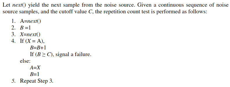
With the following criteria for failure:

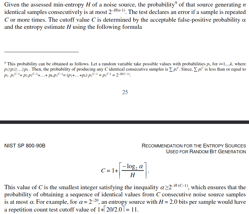
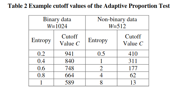
And this is the adaptive proportion test:

With the following example cutoff values:

OK, so now we know the tests. What do these even mean in the context of our TRNGs?

Ring Oscillator Implementations

Our Ring Oscillator architecture consists of 33 independent ring
oscillators that operate in two phases. In the first phase, the rings oscillate independently of each other to collect phase noise; the state of each ring is XOR’d into a state bit through snapshots taken at regular intervals. In a second phase, they are merged into a single large ring oscillator, where they then have to reach a consensus. A single bit is taken from the consensus oscillator, and progressively shifted into the state of the ring oscillator.

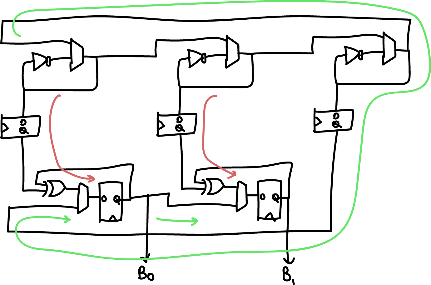
Above is a simplified “two bit” version of the generator, where instead of 33 oscillators we have 3, and instead of 32 bits of entropy we get 2. The red arrow is the flow of entropy in the first phase, and the green arrow is the flow of entropy in the second phase. The two phases are repeated N+1 bit times (33 times in the full implementation, 3 times in the simplified diagram above).

We can see from the diagram that entropy comes from the following
sources:

  • Random phase accumulated in the smaller ring oscillators due to the accumulation of phase noise during a “dwell” phase that can be set by software (nominally 1000 ns)
  • Decision noise associated with the sampling jitter of the smaller ring oscillators with an initial sampling flip-flop. Note that the ring oscillators operate at a higher frequency (~300-500MHz) than the sampling rate of the flip flops (100 MHz).
  • Global phase accumulated during the consensus process of the larger ring oscillator. The time to achieve consensus is set by a “delay” parameter that is set by software (nominally 40ns)
  • Cross-element mixing through the continuous shifting of bits to the right, and further XOR’ing of phase

The global phase consensus and cross-element mixing is quite important because ring oscillators have a tendency to couple and phase-lock due to crosstalk side-channels on both signal and power. In this architecture, each ring’s local noise conditions, including its crosstalk, is applied across each of the 32 output bits; and each ring’s oscillation is “reset” with an arbitrary starting value between each cross-element phase.

A higher rate of aggregate entropy is achieved by running four instances of the core described above in parallel, and XOR’ing their result together. In addition, the actual delay/dwell parameters are dynamically adjusted at run-time by picking some of the generated entropy and adding it to the base dwell/delay parameters.

Thus, when looking at this architecture and comparing it against the NIST spec, the question is, how do we apply the Repetition Count test and the Adaptive Proportion tests? The Repetition Count test is probably not sensitive enough to apply on the 32-bit aggregate output. It’s probably best to apply the Repetition Count and Adaptive Proportion test a bit upstream of the final generated number, at the sampled output of the ring oscillators, just to confirm that no constituent ring oscillator is “stuck” for any reason. However, the amount of logic resources consumed by adding this must be considered, since we have (33 * 4) = 132 separate oscillators to consider. Thus, for practical reasons, it’s only feasible to instrument one output from each of the four cores that is indicative of the health of the entire bank of oscillators.

Picking the right spot to instrument is tricky. The “large” ring oscillator is actually low-quality entropy, because it has a period of about 30MHz but is oversampled at 100MHz. Thus the majority of the entropy is contributed from the repeated undersampling of the “small” rings. The final sampling point chosen is the output of the sampling register after it’s “soaked up” enough entropy from the combination of a small ring and a large ring to result in a useful measurement.

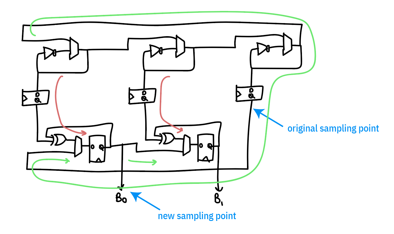
Originally, I had tried looking at the “large” oscillator only to try to find something more “raw”, under the hypothesis that we would be more likely to catch problems in the system at a less refined stage; the problem is that it was so “raw” that all we caught was problems. However, we do use this tap as a “true negative” test, to ensure that the health tests are capable of flagging an entropy source that is less than perfect.

I’m also going to introduce an extra test that’s inspired by the Runs Test in the STS suite, that I call “MiniRuns”. This test records the frequency of continuous runs of bits: 0/1, 00/11, 000/111, 0000/1111, etc. This test will offer more insight into the dominant projected failure mode of the ring oscillator, namely, it oscillating as a perfectly synchronized square wave — a condition that neither of the recommended NIST tests are capable of capturing. However, if the oscillator becomes too deterministic, we should see a shift in the distribution of run lengths out of the MiniRuns test.

Avalanche Generator Implementation

The avalanche generator consists of two avalanche diodes biased from a shared power supply, sampled by a pair of op-amps with a slight bit of gain; see our page on its theory of
operation
for details on the physics and electronic design. Here, we focus on its system integration. The outputs of each of the op-amps are sampled with a 12-bit ADC at a rate of ~1MSPS, and XOR’d together. As this sampling rate is close to the effective noise bandwidth of the diodes, we reduce the sampling rate by repeatedly shifting-by-5 and XOR’ing the results a number of times that can be set by software, nominally, 32 times into a 32-bit holding register, which forms the final entropy output. This 32x oversampling reduces the rate of the system to 31.25kHz.

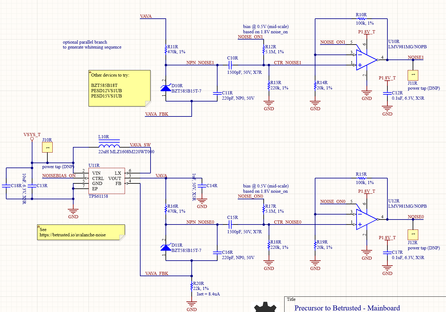
Thus in this scheme, entropy comes from the following sources:

  • The avalanche properties of two individual diodes. These are considered to be high-quality properties derived from the amplification of true thermal noise.
  • The sampling interval of the ADC versus the avalanche waveform
  • Noise inherent in the ADC itself
  • Note that the two diodes do share a bias supply, so there is an opportunity for some cross-correlation from supply noise, but we have not seen this in practice.

Because we are oversampling the avalanche waveform and folding it onto itself, what we are typically measuring is the projected slope of the avalanche waveform plus the noise of the ADC. Significantly, the SNR of the Xilinx 7-series “12-bit” ADC integrated into our FPGA is 60dB. This means we actually have only 10 “good” bits, implying that the bottom two bits are typically too noisy to be used for signal measurements. The XADC primitive compensates for this noise by offering automatic averaging over 16 samples; we turn this off when sampling the avalanche noise generators, because we actually *want* this noise, but turn it on for all the other duties of the XADC.

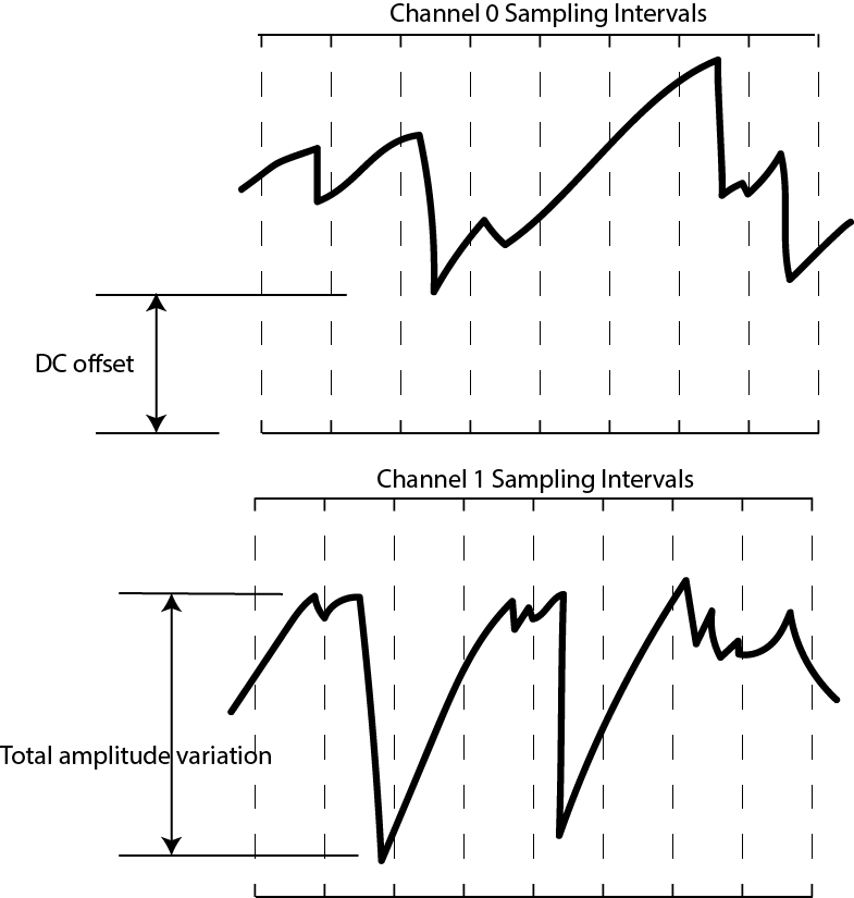
It’s also important to consider the nature of sampling this analog
waveform with an ADC. The actual waveform itself can have a DC offset, or some total amplitude variation, so naturally the LSBs will be dense in entropy, while the MSBs may be virtually constant. By focusing on the bottom 5 bits out of 12 with the 5-bit sliding window, we are effectively ignoring the top 7 bits. What does this do to the effective waveform? It’s a bit easier to show graphically:

Below is a waveform at full resolution.

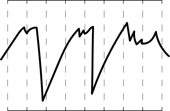
If we were to only consider 11 bits out of the 12, we effectively take half the graph and “wrap it over itself”, as shown below:

Down to 10 bits, it looks like this:

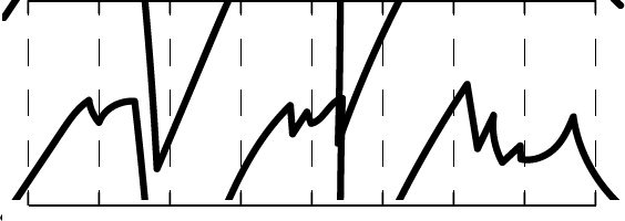
And down to 9 bits, like this:

And so forth. By the time we are down to just considering 5 bits, we’ve now taken the effective DC offset and amplitude variations and turned them into just another random variable that helps add to the entropy pool. Now take two of these, XOR them together, and add in the effective noise of the ADC itself, and you’ve arrived at the starting point for the ADC entropy pool.

In terms of on-line entropy tests, it probably makes the most sense to apply the Repetition Count test and the Adaptive Proportion tests to the bottom 5 bits of the raw ADC feed from each avalanche diode (as opposed to the full 12-bit output of the ADC). We don’t expect to hit “perfect entropy” with the raw ADC feed, but these tests should be able to at least isolate situations where e.g. the bias voltage goes too low and the avalanche effect ceases to work.

In addition to these tests, it’s probably good to have an “absolute
excursion” test, where the min/max of the raw avalanche waveforms are recorded over a time window, to detect a diode that is flat-lining due to aging effects, or a bias voltage source that is otherwise malfunctioning. This test is not suitable for catching if an attacker is maliciously injecting a deterministic waveform on top of the avalanche diodes, but is well-suited as a basic health check of the TRNG’s core mechanisms under nominal environmental conditions.

Developing

After installing the tooling necessary to build a Precursor/Betrusted SoC, I started writing the code.

Here’s the general method I use to develop code:

  1. Think about what I’m trying to do. See the first section of this
    article.
  2. Write the smaller submodules.
  3. Wrap the smaller modules into a simulation framework that shakes
    most of the skeletons out of the closet.
  4. Repeat 1-3, working your way up the chain until you arrive at your full solution.
  5. Write drivers for your new feature
  6. Slot your feature into the actual hardware
  7. Test in real hardware
  8. Continuously integrate, if possible, either by re-running your sim against every repo change or better yet recompiling and re-running your test on actual hardware.

The key to this loop is the simulation. The better your simulation, the better your outcome. By “better simulation”, I mean, the less
assumptions and approximations made in the test bench. For example, one could simulate a module by hooking it up to a hand-rolled set of Verilog vectors that exercises a couple read and write cycles and verifies nothing explodes; or, one could simulate a module by hooking it up to a fully simulated CPU, complete with power-on reset and multiple clock phases, and using a Rust-based framework to exercise the same reads and writes. The two test benches ostensibly achieve the same outcome, but the latter checks much more of the hairy corner cases.

For Betrusted/Precursor, we developed a comprehensive simulation framework that achieves the latter scenario as much as possible. We simulate a full, gate-level Vex CPU, running a Rust-built BIOS, employing as many of the Xilinx-provided hardware models as we can for things like the PLL and global power-on reset.

Demo

This is the point in the cooking show at which we put the turkey into an oven, say something to the effect of “…and in about five hours, your bird should be done…” yet somehow magically pull out a finished turkey for carving and presentation by the time we finish the sentence.

So: after a bunch more driver-writing and breaking out signals to gain visibility into the various metrics and failure modes, we can see the on-line health tests in action.

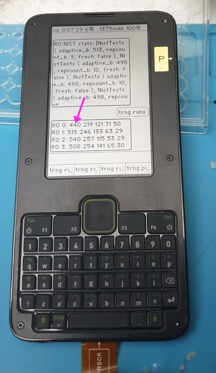
Above is an example of the trng test data output on Precursor, set where `RO 0` is connected to the “large” oscillator that runs too slowly (serving as a “true negative” test), and the others are connected to the final output tap for the test (serving as a “true positive”). In the output, you can see the four ring oscillators (numbered 0-3) with the frequency of each of five run lengths printed out. `RO 0` has a significant depression in the count for the run-length 1 bin, compared to the other oscillators (440 vs 515, 540, and 508).

One final detail is implementing an automated decision mechanism for the MiniRuns test. Since the MiniRuns test wasn’t from the NIST suite, I couldn’t simply read a manual to derive a threshold. Instead, I had to consult with my perlfriend, who also happens to be an expert at statistics, to help me understand what I was doing and derive a model that could help me set limits. Originally, she suggested a chi-square test. This would be great, but the math for it would be too complicated for an automated quick power-on test. So, we downgraded the test to simple max/min thresholds on the counts for each “bin” of runs. I used a similar criteria to that suggested in the NIST test, that is, š›‚ = 2^-20, to set the thresholds, and baked that into the hardware code. Here’s a link to the original spreadsheet that she used to compute both the chi-square and the final, simpler min/max tests. One future upgrade could be to implement some recurring process in Xous that collects updated results from the MiniRuns test and does the more sophisticated chi-square tests on it; but that’s definitely a “one for the road” feature.

Closing Thoughts

The upshot is that we now have all the mandatory NIST tests plus one each “tailored” tests for each type of TRNG. Adding the MiniRuns automated criteria increased utilization to 56.5% — raising the total space used by the tests from about 2% of the FPGA to a bit over 4%. The MiniRuns test is expensive because it is currently configured to check for runs ranging from length 1 to 5 over 4 banks of ring oscillators — so that’s 5 * 4 * (registers/run ~30?) = ~600 registers just for the core logic, not counting the status readout or config inputs.

Later on, if I start running out of space, cutting back on some of the instrumentation or the depth of the runs measured might be a reasonable thing to do. I would suggest disposing of some of the less effective NIST tests entirely in favor of the home-grown tests, but in the end I may have to kick out the more effective supplemental tests. The reality is that it’s much easier to defend keeping inferior-but-spec-compliant tests in the system, rather than opting for superior tests at the expense of the specification tests.

That’s it for part 1. If you’re super-eager to read more, you can read the full wiki entry on data conditioning for the TRNG at the Precursor/Betrusted documentation wiki. Or, you can just wait until I get around to chopping the page down to size and repackaging it into a more bite-side blog entry.

Upgrading Precursor’s TRNG

Monday, June 14th, 2021

It was pointed out that we’re missing a step-by-step guide on how to go from an idea, to hardware, to a fully implemented feature in Xous for Precursor. So, here it is.

Because Precursor uses an FPGA for its SoC, we can add new features to the hardware ā€œon the flyā€. In this case, weā€™re going to add some improvements to our basic managed TRNG block. To review, the existing TRNG consists of an avalanche noise source and a ring oscillator noise source as hardware-based sources of ā€œtrueā€ entropy. Two generators are used for the following reasons:

  • An external discrete generator is easy to check (just put an oscilloscope on the avalanche noise source), but harder to protect against physical access attacks
  • An integrated, on-chip generator is harder to hack (more robust against a pair of tweezers executing a short-to-ground attack, or RF interference attacks), but harder to check (is the data from the TRNG, or merely a decoy CSPRNG implant?)
  • All hardware mechanisms are fallible; having two sources improves robustness against transient drop-outs or aging failures

We’ve already done extensive, months-long characterization of both of the TRNG sources and found them to produce passable raw entropy. However, the system is still missing two features that are generally considered to be best practice:

  1. Independent, on-line health monitors of the raw TRNG outputs. Itā€™s important that the health monitoring happens before any conditioning or mixing of the raw data happens, and significantly, there is no one-size-fits-all health monitor for a TRNG: itā€™s advised (NIST SP 800-90B sec 4.4) to have tests that are tailored to the noise source.
  2. Conditioning of the raw data. Despite best efforts to make TRNGs unbiased and flawless, they are really hard to get right. Furthermore, they are only capable of producing high-quality entropy at a limited data rate. Thus, most practical systems take a TRNG output and run it through a cryptographic stream cipher to generate a final datastream; this simultaneously protects against minor flaws in the TRNG while improving the availability of random numbers.

The following lengthy posts walk step-by-step through the thought process, implementation and debugging process of adding these features. Few people would even notice these features, and if everything is doing its job right (that is, the TRNG’s raw data is working correctly) is indistinguishable from the state before all this effort. However, we take TRNGs seriously here; so much rides on the quality of these random numbers that it’s probably worth the effort to harden them against failures, be they unintentional, malicious, or just design bugs.

I have to be honest, I spent a lot of time to check a box that few people care about, but Iā€™ve come to realize thatā€™s mainly what writing OS code and firmware is about. You can get more fame and dopamine from creating a cool UI theme with an afternoon of work. Itā€™s also really hard to explain to everyday people what youā€™re doing exactly with all this time and effort; but without the underlying frameworks that make things durable and reliable, we all might as well be drawing chalk pictures on the side walk.

Without further ado, here are the two guides for adding features, there’s some repetition between the posts so they can be read independently.

I’ll also take highlights from these wiki articles and repost them to the blog here, creating a “TL;DR” version that is also neatly delivered to the inboxes of my blog’s email subscribers.

What’s the Value of Hackable Hardware, Anyway?

Friday, December 11th, 2020

There is plenty of skepticism around the value of hackable products. Significantly, hackability is different from openness: cars are closed-source, yet support vibrant modding communities; gcc is one of the ā€œreal OGā€s of open source, but few users find it easy to extend or enhance. Is it better to have a garden planted by the most knowledgeable botanists and maintained by experienced gardeners, or an open plot of land maintained by whoever has the interest and time?


Above left: Walled garden of Edzell Castle; above right: Thorncliffe Park community garden.

In the case of hardware products, consumer behavior consistently affirms a strong preference for well-curated gardens. Hardware is hard ā€“ not only is it difficult to design and validate, supply chains benefit from economies of scale and predictable user demand. The larger a captive audience, the more up-front money one can invest into developing a better hardware product. However, every decision to optimize comes with inherent trade-offs. For example, anytime symmetry is broken, one must optimize for either a right-handed or a left-handed version.


Above: touching the spot indicated by the red arrow would degrade antenna performance on an iPhone 4. This spot would naturally rest on the palm of a left-handed user. Image adapted from “iPhone 4” by marc.flores, licensed under CC BY 2.0.

Some may recall a decade ago when the iPhone 4 was launched, left-handed people noticed the phone would frequently drop calls. It turned out the iPhone 4 was designed with a critical antenna element that would fail when held naturally by a left-handed person. The late Steve Jobs responded to this problem by telling users to ā€œjust avoid holding it that wayā€. Even if he didnā€™t mean it, I couldnā€™t help but feel like he was saying the iPhone 4 was perfect and left-handers like me were just defective humans who should be sent to re-education camps on how to hold things.

Of course, as a hardware engineer, I can also sympathize with why Steve Jobs might have felt this way ā€“ clearly, a huge amount of effort and thought went into designing a technical masterpiece that was also of museum-quality construction. Itā€™s frustrating to be told, after spending years and billions of dollars trying to build ā€œthe perfect productā€ that they somehow got it wrong because humans arenā€™t a homogeneous population. Rumors have it Apple spent tens of millions of dollars building micron-precision production jigs out of injection-molding grade tooling to ensure the iPhone4 was simply perfect in terms of production tolerances; duplicating all of those to make a mirror-image version for left-handers that make up 10% of the market size just made no business sense. It proved to be cheaper and easier, ultimately, to take full refunds or to give out rubber bumpers to the users who requested them.

I do think there is such a thing as ā€œover-designingā€ a product. For example, contemporary ā€œhigh conceptā€ smartphone design is minimalist ā€“ phone companies have removed headphone jacks, hidden the front camera, and removed physical buttons. There is clearly no place for screws in this world; the love affair of smartphones and adhesives has proven to be … sticky. Adhesives, used in place of screws in modern smartphones, are so aggressive that removing them either requires additional equipment, such as a hot plate and solvents, or simply destroying the outer bezel by breaking the outer case off in pieces and replacing it with an entirely new bezel upon re-assembly. In other words, hacking a modern smartphone necessarily implies the destruction or damage of adhesive-bound parts.

With Precursor, Iā€™m bringing screws back.

Precursorā€™s screws are unapologetic ā€“ I make no attempt to hide them or cover them with bits of tape or rubber inserts. Instead, Iā€™ve sourced custom-made Torx T3 metric screws with a black oxide finish that compliments the overall color scheme of Precursor. Six of them line the front, as a direct invitation for users to remove them and see whatā€™s inside. Iā€™ve already received ample criticism for the decision to show screws as ā€œprimitiveā€, ā€œuglyā€, ā€œout of touch with modern trendsā€ — but in the end, I feel the visual clutter of these six screws is a small price to pay for the gain in hackability.

Of course, the anti-screw critics question the value of hackability. Surely, I am sacrificing mass-market appeal to enable a fringe market; if hackability was so important, wouldnā€™t Apple and Google already have incorporated it into their phones? Wouldnā€™t we see more good examples of hackability already?

This line of questioning is circular: you canā€™t get good examples of hacks until you have made hackable products wide-spread. However, the critics are correct, in a way: in order to bootstrap an ecosystem, weā€™re going to need some good examples of why hackability matters.

In the run-up to crowdfunding Precursor, I was contemplating a good demo hack for Precursor. Fortuitously, a fellow named Matt Campbell opened a GitHub issue requesting a text-to-speech option for blind users. This led me to ask what might be helpful in terms of a physical keyboard design to assist blind people. You can read the thread for yourself, but Iā€™ll highlight that even the blind community itself is divided on whether or not there is such a thing as the ā€œblind ghettoā€ — an epithet applied by some users who feel that blindness-specific products tend to lag behind modern smartphones, tablets, and laptops. However, given that most modern gadgets struggle to consider the needs of 10% of the population thatā€™s left-handed, Iā€™m readily sympathetic to the notion that gadgets make little to no concession to accommodate the even smaller number of blind users.

Matt was articulate in specifying his preferred design for a pocketable keyboard. He referred me to the ā€œBraille ā€˜n Speakā€ (shown above) as an example of an existing braille keyboard. Basically, it takes the six dots that make up braille, and lines them up horizontally into three left and three right sets of buttons, adding a single button in the middle that functions as a space bar. Characters are entered by typing chords that correspond to the patterns of the six dots in the braille alphabet. Not being a braille user myself, I had to look up what the alphabet looked like. I made the guide below based on a snippet from Wikipedia to better understand how such a keyboard might be used.

Ironically, even though Matt had linked me to the picture of the Braille nā€™ Speak, it still took a while to sink in that a braille variant of Precursor did not need a display. Iā€™m a bit ashamed to admit my first sketches involved trying to cram this set of switches into the existing keyboard area of the Precursor, without first removing the display entirely. I had to overcome my own prejudice about how the world should look and it took me time and empathy to understand this new perspective.

Once I had a better grasp of Matt’s request, I set about designing a customized braille variant. Precursor was designed for this style of hacking: the keyboard is a simple 2-layer PCB thatā€™s cheap and easy to re-design, and the front bezel is also a PCB, which is a bit more expensive to redesign. Fortunately, I was able to amortize setup costs by bundling the braille front bezel variant with another variant that I had to fabricate anyways for the crowdfunding campaign. Beyond that, I also had to come up with some custom key caps to complement the switches.

The major challenge in designing any type of mobile-friendly keyboard is always a trade-off between the hand feel of the switches, versus thinness of the overall design. On one side of the spectrum, full-travel mechanical switches have a wonderful hand feel, but are thicker than a sausage. On the other side of the spectrum, dome switches and printed carbon ink patterns are thinner than a credit card, but can feel mushy and have a limited ā€œsweet spotā€ — the region of a key switch with optimal tactile feedback and operational force curves. The generally well-regarded Thinkpad keyboards go with a middle-ground solution thatā€™s a few millimeters thick, using a ā€œscissorā€ mechanism to stabilize the key caps over a silicone dome switch, giving individual keys a bit of travel while ensuring that the ā€œsweet spotā€ covers the entire key cap. Optimizing key switch mechanisms is hard: some may recall the controversy over Appleā€™s re-design of the MacBookā€™s keyboard to use a ā€œbutterflyā€ mechanism, which shaved a couple mm of thickness, but led to lawsuits over a defect where the keyboard allegedly stopped working when small bits of dust or other particles got trapped under it.

Given the short time frame and a shoestring budget, I decided to use an ultra-thin (0.35mm) tactile switch that I could buy off-the-shelf from Digikey and create custom key caps with small dimples to assist users in finding the relatively small sweet spots typical of such switches. I have sincere hopes this is a pretty good final solution; while it lacks a scissor mechanism to spread off-centered force, the simple mechanism meant I didnā€™t have to stick with a square key cap and could do something more comfortable and ergonomic to focus forces into the sweet spot. At the very least, the mechanism would be no worse than the current mechanism used in Precursorā€™s existing keyboard for sighted users, which is similarly a dome switch plus a hybrid-polymer key film.

Next, I had to figure out where to place the switches. To assist with this, I printed a 1:1 scale version of the Precursor case, dipped my fingertips in ink, and proceeded to tap on the printout in what felt like a natural fashion.

I then took the resulting ink spots and dimensioned their centers, to place the centroid of each key cap. I also asked my partner, who has smaller hands, to place her fingers over the spots and noted the differences in where her fingers lay to help shape the final key caps for different-sized hands.

Next, using the ā€œmaster profileā€ discussed in the previous post on Precursorā€™s mechanical design, I translated this into a sketch to help create a set of key caps based on splines that matched the natural angle of fingers.

Above, you can see an early sketch of the key caps, showing the initial shape with dimples for centering the fingers.

Before moving ahead and spending a few hundred dollars to build a functional prototype, I decided to get Mattā€™s feedback on the design. We submitted the design to Shapeways and had a 3D print sent to Matt, which he graciously paid for. After receiving the plastic dummy, his feedback was that the center space bar should be a single key, instead of two separate keys, so I merged the two separate key caps of the space bar together into a single piece, while retaining two separate switches wired in parallel under the space bar. I felt this was a reasonable compromise that would allow for a ā€œsweet spotā€ that serviced lefties as well as righties.

I then re-designed the keyboard PCB, which was a fairly simple task, because the braille keyboard consists of only eight switches. I just had to be careful to pick row/column pairs that would not conflict during chording and be sure to include the row/column pairs necessary to turn Precursor on after being put to sleep. I also redesigned the bezel; eliminating the display actually makes manufacturing a little bit easier because it also removes a beveling step in the manufacturing process. I kept the RF antenna in exactly the same location, as its design was already well-characterized and it takes a lot of effort to tune the antenna. Finally, I decided to manufacture the key switches out of aluminum. The switches have a lot of fine features and I needed a stiff material that could translate off-target force to the key switches to enlarge the sweet spot as much as possible.


Above: The prototype of Precursor with braille keyboard.

About three weeks later, all the parts for the braille keyboard had arrived. I decided to use purple anodization for the key switches which, combined with the organic key shapes, gives the final design a bit of a Wakanda-esque ā€œBlack Pantherā€ aesthetic, especially when mounted in a brass case. The key switch feel is about in line with what I imagined, with the caveat that one of the switches feels a little less nice than the rest, but I think thatā€™s due to a bad solder job on the switch itself. I havenā€™t had a chance to trace it down because…well, Iā€™ve had to write a bunch of posts like this to fund Precursor. I have also been working with Xobs to refactor Xous in hopes of putting together enough code to send Matt a prototype he can evaluate without having to write gobs of embedded hardware driver code himself.

Above is a quick photo showing the alignment of fingers to keys. Naturally, itā€™s perfect for my hand because it was designed around it. Iā€™m looking forward to hearing Mattā€™s opinion about the feel of the keys.

Above is a photo of the custom parts for the braille keyboard. At the top, you can see the custom bezel with key caps and the RF antenna matching circuitry on the top right. On the bottom, you can see the custom keyboard PCB mounted onto a Precursor motherboard. The keyboard PCB is mostly blank and, because of the small number of keys and the flexibility of the FPGA, thereā€™s an option to mount more peripherals on the PCB.

Despite not being yet finalized, I hope this exercise is sufficient to demonstrate the potential value of hackable products. The original design scope for Precursor (nƩe Betrusted) did not explicitly include a braille keyboard option, but thanks to modular design principles and the use of accessible construction materials, I was able to produce a prototype in about a month that has a similar fit and finish as the mainstream product.

As long as humans choose to embrace diversity, I think hackability will have value. A notional ā€œperfectā€ product implies thereā€™s such a thing as a ā€œperfectā€ user. However, in reality, even the simple conundrum of left- or right-handedness challenges the existence of a singular ā€œperfectā€ product for all of humanity. Fortunately, accommodating the wonderfully diverse, quirky, and interesting range of humanity implicates just a few simple engineering principles, such as embracing screws over adhesives, openness, and modularity. That we canā€™t hack our products isnā€™t a limitation of physics and engineering. Precursor demonstrates one can build something simultaneously secure and hackable, while being compact and pocketable. This suggests the relative lack of hackable products on the market isnā€™t a fundamental limitation. Maybe we just need a little more imagination, maybe we need to be a little more open-minded about aesthetics, and maybe companies need to be willing to take brave steps toward openness and inclusivity.

For Apple, true ā€œcourage to move on and do something new that betters all of usā€ was to remove the headphone jack, which resulted in locking users deeper into a walled-garden ecosystem. For hackers like myself, our ā€œcourageā€ is facing blunt criticisms for making ā€œuglyā€ products with screws in order to facilitate mods, such as braille keyboards, in order to expand the definition of ā€œall of usā€ beyond a set of privileged, ā€œperfectā€ users.

I hope this braille keyboard is just the first example of many mods for Precursor that adapt the product for unique end-users, bucking the trend of gaslighting users to mold their behavior and preferences to fit the product. If youā€™ve got an itch to develop your own yet-to-be-seen feature in a mobile device, please visit our crowdfunding campaign page to learn more about Precursor. Weā€™re close to being funded, but weā€™ve only a few days left in the campaign. After the campaign concludes on December 15th, the limited edition will no longer be available, and pricing of the standard model goes up. If you like what you see, please consider helping us to bring Precursor to life!

Precursor’s Mechanical Design

Monday, December 7th, 2020

ā€œPocketabilityā€ is the difference between Precursor and naked PCB FPGA development platforms. We hope Precursorā€™s pocketability helps bring more open hardware out of the lab and into everyday use. Thus, the mechanical design of Precursor is of similar importance to its electrical, software, and security design.

We always envisioned Precursor as a device that complements a smartphone. In fact, some of the earliest sketches had Precursor (then called Betrusted) designed into a smartphoneā€™s protective case. In this arrangement, Precursor would tether to the phone via WiFi and the always-on LCD for Precursor could then be used to display static data, such as a shopping list or a QR code for a boarding pass, giving Precursor a bit of extra utility as a second screen thatā€™s physically attached to your phone. However, there are too many types of smartphones out there to make ā€œPrecursor as a phone caseā€ practical, so we realized it would make more sense to make Precursor a ā€œstand-alone deviceā€.

As such, we wanted Precursor to be unobtrusive and thin in order to lighten the burden of carrying a secondary security device. Our first-draft EVT design had Precursor at just 5.7 mm thick, placing it among the ranks of the thinnest phones. Unfortunately, the EVT device had no backlight on the LCD, which made it unusable in low-light conditions. Increasing the final thickness to 7.2 mm allowed us to introduce a backlight, while still being slimmer than every iPhone since the iPhone 8.

To minimize the thickness of Precursor, I first divided the design into major zones, such as the main electronics area, the battery compartment, the vibration motor, and the speaker. I then estimated the overall thickness of components in each zone and optimized the thickest one by either re-arranging components or making component substitutions until another zone dominated the overall thickness.


A cross-section view of the final Precursor design, calling out the dimensions of the various vertical height zones of the design.

After considering about a dozen or so mechanical layout scenarios, we arrived at the design shown above. Like every modern mobile device, when viewed by size and weight, Precursor is basically a battery attached to a display.

The practical limit on battery thickness is driven by the overhead of the protective wrapping around the battery. Lithium-polymer ā€œpouchā€ batteries rapidly decline in energy density with decreasing thickness as the protective wrapper around the battery starts to factor appreciably into its overall thickness. The loss of energy density becomes appreciable below 3.5mm, and so this fixed the batteryā€™s thickness at 3.5mm, plus about 0.2mm allowance for any swelling that might happen plus adhesive films.


Teardown view of Precursorā€™s LCD with backlight attached. Note that to inspect the transistors inside the LCD, the backlight module needs to be removed.

Display thickness is limited by the thickness of the liquid crystal (LC) ā€œcellā€, plus backlight. Fortunately, LC cells are extremely thin, as they are basically just the glass sheets used to confine a microscopic layer of liquid crystal material, plus some polarizer films ā€“ in Precursorā€™s case, the LC cell is just 0.705mm thick. The backlight is substantially thicker, as it requires a waveguide plus a film stack that consists of two brightness enhancing films, a diffuser sheet, adhesives, and its own protective case to hold the assembly together, leading to a net thickness increase of roughly 1.3mm. The backlight itself is actually a full-custom assembly that we designed just for Precursor; itā€™s not available as an off-the-shelf part.

With the display and battery thicknesses defined, the final thickness of the product is determined by the material selection of the protective case. We use aluminum for the bottom case and FR-4 for the bezel (we discuss the bezel in a previous post).

Using aluminum for the bottom case allows us to shave about 1 mm (~15%) of thickness relative to using a polymer like ABS or PC at the expense of a fairly substantial increase in per-unit manufacturing costs. Although polymers are about twice the cost of aluminum by weight, an aluminum case costs about 10x as much to produce. This is because polymers can be molded in a matter of seconds, with very little waste material, whereas aluminum must be CNCā€™d out of a slab in a time-consuming process that scraps 80% of the original material. Surprisingly, the 10x cost-up isnā€™t the waste material; there is an efficient market for buying and recycling post-machining aluminum. Most of the extra cost is due to the labor required to machine the case which is orders of magnitude longer than the time required for injection molding.

Thus, while we could have made Precursor cheaper, we felt it would both be more pocketable, as well as more desirable, with the machined aluminum case: it would look more like a high-end mobile device, instead of a cheap plastic toy or remote control.

Using aluminum also allows us to play some fun tricks with the fit and finish of the product, thanks in part to the transformative effect Apple had on the mobile phone industry. Their adoption of CNC machining as a mass production process sparked a huge investment in CNC capability, making once-exotic processes more affordable for everyone. A good example of this is the single-crystal diamond cutting process for making shiny beveled edges. This used to be a fairly expensive specialty process, which you can read more about in this great thesis on ā€œPrecision and Techniques for Designing Precision Machinesā€ by Layton Carter Hale which, on page 27, describes the Large Optics Diamond Turning Machine (LODTM). The LODTM relies on the raw precision achievable with a diamond bit to create geometries for mirrors without the need for post-polishing.


A single-crystal diamond bit, courtesy of Victor from Jiada

I first learned about this technique in 2017, when I brought a Xiaomi aluminum mouse pad with a mirror-finish bevel.


Bevel on the Xiaomi mousepad

Despite a sub-$20 price tag, the mirror-finish bevel gave it quite an expensive look. Polishing to a mirror finish is a time consuming task, so I became curious about how this could be economical on a humble mouse pad. I bought another mouse pad, and brought it to Prof. Nadya Peek, and asked her how she thought it was fabricated. Readers who are familiar with our Novena laptop may recall her name as the designer of the Peek Array for mounting accessories inside the Novena. Iā€™ve been lucky to have her mentorship and advice on all things mechanical engineering for many years now. So many of my products are better thanks to her!

She took one look at the bevel and immediately guessed it was cut by a single-crystal diamond bit, but she could do even better than making a guess. At the time, she was still a graduate student at the MIT Center for Bits and Atoms, where she had a Hitachi FlexSEM 1000 II equipped with the X-ray composition analysis option at her disposal. So, she took the mouse pad to the machine shop, chopped a corner off with a band saw, and loaded it into the SEM.


Viewing the output of the composition analysis.

If you zoom into the screen on the right, you can see the X-ray composition analysis reveals an unusually high amount of carbon on the aluminum surface (~10% by weight). Unlike iron, carbon is not commonly used in alloying aluminum. In this case, the chief alloying element seems to be magnesium, implying that the mousepad is probably a 5000-series alloy (perhaps 5005 or 5050). Given this, it seemed reasonable to conclude that the carbon residue on the beveled surface is direct evidence of a diamond cutting bit.


The shiny beveled edge on Precursor is brought to you by a single-crystal diamond milling bit.

Armed with this knowledge, I was able to work with Victor, the owner of Jiada ā€“ the primary CNC provider for Precursor ā€“ to specify a diamond-bit beveling process that brings you the nice edge finish on the final Precursor product. I also count Victor as one of my many mechanical design mentors; heā€™s one of those practicing-engineer-as-CEO types who has applied his extensive knowledge of mechanical engineering to open his own CNC and injection molding business. He always seems up for the challenge of developing new and interesting fabrication processes. Thatā€™s why Iā€™ve been working closely with Victor to develop the campaign-only omakase version of Precursor.

Because Precursorā€™s case is CNC, weā€™re not limited to aluminum as the base material. Itā€™s primarily a matter of cost and yield to manufacture with other materials. We could, for example, machine the case out of titanium, but the difficulty of machining titanium means we would likely have to machine two or three cases to yield a single one that passes all of our quality standards. This, combined with the high cost of raw titanium, would have added about a thousand dollars on to the final price of the omakase Precursor and we felt that would be just too expensive. Thus, Victor and I are currently evaluating two material candidates: one is physical vapor deposition (PVD)-finished stainless steel, the other is naval brass. These material choices were heavily influenced by Prof. Peekā€™s opinions. (It’s a coincidence the recently launched iPhone 12 uses PVD stainless steel for its case, as we have been working on this project since well before the details of iPhone 12 were publicly known.)

While both the PVD steel and naval brass are much more expensive than aluminum, they have a terrific hand feel and excellent machinability. Aesthetically, the main difference between the two is the color: for the stainless steel PVD, weā€™d be going with a high-gloss, polished black look, and for the naval brass weā€™re considering a brushed finish. The naval brass is more distinctive, but the soft metal is easy to scratch; a highly polished brass surface starts to look much less nice after a week or two of banging around in your pocket. A brushed finish hides such scratches and fingerprints better and over the course of years it should develop a handsome patina.

The major downside of the naval brass is that itā€™s highly conductive. Both the PVD stainless steel and anodized aluminum inherently have a tough, non-conductive surface layer; the naval brass does not. This is particularly concerning because if any of the internal battery connections get frayed, it could lead to a fire hazard. Iā€™m currently working to see if I can find a surface coating that adequately protects the inside of the naval brass case from short circuits, but if I canā€™t find one, that may definitively rule out the naval brass option, leaving us with a PVD stainless steel case for the omakase version.

While good looks and a nice hand feel are significant benefits of going with a CNC process, another important reason I picked CNC over injection molding is anyone could build a full-custom version of a Precursor case in single quantities, with no compromise on finish quality or durability. Unlike the situation of injection molding versus 3D printing, which either use radically different base materials (for SLA 3D printing) or processes (for FDM 3D printing), your custom case can be made in single quantities with the exact same metal alloys and the exact same processes used in production Precursors.

This trait is particularly important for a mobile device and not just because the design works better when itā€™s built using its originally intended material system. Itā€™s also because mobile devices donā€™t have a lot of extra space to devote to expansion headers and breakout boards. While it is beyond the level of a weekender hobby project to make a custom case, itā€™s probably within the scope of an undergraduate-level research project to undertake the necessary revisions to, for example, thicken the case and incorporate a novel medical sensor or a new kind of radio. In order to facilitate easier modifications to the caseā€™s native Solidworks design file, I use a ā€œmaster profileā€ to define the case body, bezel, and ā€œribbonā€ (the outer band that defines the height of the case). Helena Wang, another friend to whom I turn to for advice on mechanical design, taught me about the general technique of top-down modeling and using master profiles. Top-down modeling pushes a lot of design work into the up-front structure and planning of the 3D body in exchange for being able to revise the model without having to resolve dozens of conflicting downstream mechanical constraints. For example, when I realized I had to modify the case to be 1.5mm thicker to accommodate the backlight for the LCD, I was able to make the necessary change by just adjusting a single dimension in the ribbon height master profile, followed up by perhaps a half hour of cleaning up the offsets on structures which were defined outside of the master profile, such as the mounting points used to support the keyboard and the polymer radome that allows the WiFi signal out from the metal case.


A screenshot of the CAD tool view of the Precursor case, highlighting the master profile that defines the outer dimensions of the case.

Of course, making edits to the master profile requires access to a copy of Solidworks, which is not an open source tool; but FreeCAD users are welcome to redraw the design in their native format! Iā€™ve heard good things about FreeCAD, but I just havenā€™t had the time to learn a new design tool. For smaller modifications that donā€™t involve changing major dimensions of the case ā€“ such as adding some extra through-holes for sensors or internal mounts for additional circuit boards ā€“ the case design is also available in a tool-neutral STEP format. Every CAD tool I know of can accept STEP format and, since it is actually the format used for CNC fabrication, itā€™s by definition sufficient for creating copies of the case.

If youā€™ve read my posts over the years, you may have noticed that Iā€™ve never taken a formal course on mechanical engineering. Everything I know has been either gleaned from taking things apart, touring factories, scouring the Internet, and perhaps most importantly receiving advice from friends and mentors like Nadya, Victor, and Helena. Itā€™s been a wonderful journey learning how things are made, I hope posts like this and the associated design files will aid anyone who wants to learn about mechanical design, so they may have an easier time of it than I did. Most of all, Iā€™m hoping applying my experience and making Precursor pocketable and hackable will enable more open source technology to make it out of the lab and into everyday use, without requiring anyone to learn about mechanical design.

Thanks again to all our backers for bringing us closer to our funding goal! At the time of posting, weā€™re just at 90% funded, but weā€™re also getting down to the last week to wrap things up. We need your support to get us over the 100% mark. We recognize that these are difficult, trying times for everyone, but even small $10 donations inch us toward a successful campaign. Perhaps more importantly, if you know someone who might be interested in Precursor, weā€™d appreciate your help in spreading the word and letting them know about our campaign. With your help, hopefully weā€™ll blow past our funding goal before the campaign ends, and we can begin the hard but enjoyable work of building and delivering the first run of Precursor devices.

Precursor’s Custom PCBs

Tuesday, December 1st, 2020

While the last few updates about Precursor have focused on evidence-based trust and security, this update is more about the process of making Precursor itself. There is an essential link between evidence-based trust and understanding the manufacturing process: to convince yourself that something has been constructed correctly, itā€™s helpful to understand the construction process itself. Itā€™s hard to tell if a small crack in a wall is the result of harmless foundation settling, or a harbinger of a buildingā€™s imminent collapse, without first understanding the function and construction of that wall.

Most designers like to abstract the PCB away as a commodity service, preferring ā€œno-touchā€ or ā€œone-clickā€ ordering services where design files are uploaded and finished boards arrive in the mail, on time and at a good price. This is a bit like running a restaurant and ordering your produce from a mass distributor. The quality is uniform, delivery times are good, and the taste is acceptable. However, itā€™s hard to make a dish thatā€™s really differentiated when basic ingredients all come from the same place.

I personally enjoy building electronics with a bit more of an artisanal flavor. Just as gourmet chefs invest the effort to develop relationships with their farmers, Iā€™ve developed a personal relationship with my preferred PCB shop, King Credie. Since a PCB is at the core of virtually everything I build, I have found developing a healthy personal relationship with my PCB supplier has the benefit of raising the bar on virtually all my products. While King Credie is neither the cheapest nor the quickest-turn of PCB shops, their quality is consistent and, most importantly, they are willing to customize their process. For a small shop, they offer a wide variety of speciality processes, such as rigi-flex, metal core, edge plated cavities, HDI, and custom soldermask colors.

The Precursor Bezel

The bezel for Precursor, shown below, is a good example of how this flexibility can be used in practice. The front surface of Precursor is actually a raw FR-4 PCB while the Precursor logo is a 2.4GHz antenna. The two small black dots in the logo beneath the ā€œPā€ are the antenna feed and ground stub vias, respectively, for a ā€œPIFAā€ (planar inverse F)-style antenna. The PCB itself has been countersunk, beveled, and step-milled so it can function simultaneously as a mechanical bezel, an RF antenna, and a circuit board for electrical components.

Above is an inside shot of the bezel displaying step-milling and electrical circuitry on the inside surface of the bezel PCB. The back side components are for antenna impedance matching circuitry, connector, and ESD protection. A shiny layer of clear soldermask is applied, and you can clearly see the glass weave that forms the structure of FR-4 in the step-milled areas where material is removed. This constrains the LCDā€™s location and makes space for cables and keyboard components.

Example of a milling machine at King Credie (image courtesy Chris ā€˜Akibaā€™ Wong).

Although step-milling and countersinking are not considered ā€œstandardā€ processes for PCB manufacture, it turns out that all PCBs go through a milling (or routing) process anyways. This process defines their final shape by cutting them out of a larger mother panel. Above is a photo of such a machine doing edge routing. Here, the PCB panels are stacked about five or six panels high and a routing bit is defining the final outline of each of the smaller PCBs. Since the PCB shop already has several types of precision CNC machines that can do both routing and milling, getting countersinks and step-milling done is mostly a matter of buying the correct bits and convincing the shop to do it.

That last point is tricky: since most PCB shops compete solely on price, any disruptions in tooling can lead to costly mistakes. For example, if a machine was configured for countersinking but then the operator forgot to reconfigure it for routing, the machine might have the wrong bit installed for the next operator, and a whole panel would be lost at the final stage of production! Thus the risk of small process tweaks can be amplified by ripple-effects onto other volume processes.

Fortunately, King Credie has a pricing model where they largely separate the cost to set up a manufacturing run from the cost of production. Thus, for a highly bespoke PCB like this, I might pay a few hundred dollars to set up a production run, yet just a few bucks for the raw FR-4 material. The good news is that once the new process is finalized, the cost amortizes well over a production run the size of Precursorā€™s.

Of course, specifying such a bespoke processes is also a challenge. There isnā€™t a standard (that Iā€™m aware of!) for communicating these types of things to a PCB shop, so Iā€™ve mainly resorted to ad-hoc drawings on mechanical layers in my design tool.

Above is an example of how the bezel is specified to the manufacturer. Because of the complex 2.5D topology of this PCB, I also include several cross-sections to help clarify the drawings. I also try to make it so that the gerber lines are specifying either direct tooling paths or keep-outs (as opposed to using fills and polyregions and leaving it up to the shop to define a tool path within these regions).

Above: A King Credie engineer reviews and edits a customerā€™s design (image courtesy Jin Joo ā€˜Jinxā€™ Lee).

Of course, thereā€™s a lot of email back-and-forth with the PCB shop to clarify things, and it takes an extra week to process the boards, But, itā€™s very important not to rush the shop when specifying highly bespoke designs because you want the best machine operators to run your boards, not just the ones who happen to be available that day. When things get really challenging, I know that King Credieā€™s CEO will personally go on the line to supervise production, but this is only possible because I let them prioritize correct results over fast turn delivery ā€“ heā€™s a busy guy, but itā€™s well worth the wait to get his personal assistance. Heā€™s an engineer at heart and he knows the companyā€™s capabilities like the back of his hand. And finally, it helps if I make it clear to the shop that for risky production runs like this, I will pay 100% of the quoted price, even if the scrap rate is high and they can only do a partial delivery. That being said, Iā€™ve rarely been in a situation where the shop has had to adjust delivery quantities because of yield issues. I was lucky in that the bezel process worked on the first try (subsequent iterations were around refining the antenna shape and cosmetic details), but Iā€™ve definitely had challenging PCBs where Iā€™ve had to pay for two or three goes at process development before I had a process that worked right and yielded well.

The Precursor Mainboard

Thereā€™s another aspect of PCB manufacturing that is fairly ubiquitous yet surprisingly rare in the open source hardware world: microvias.

Above is a cross-section view of the Precursor PCB, lined up against a design view of the same. Here, the PCB has been cut through a ground pad for the wifi antenna, showing a stack of two laser-drilled microvias on top of a mechanically drilled via. As you can see from this image, two microvias can fit side-by-side in the area of a standard mechanically drilled via. To put it in solid numbers, the microvias here have a hole size of 0.1mm and an annulus of 0.2mm; and the mechanical via has a hole size of 0.25mm and an annulus of 0.5mm.

This style of via is absolutely essential in handheld products with space-conscious packaging featuring typical pitches of around 0.4mm for balls on a WLCSP.

Above is an example of one such WLCSP used on Precursor. The distance between each of the small round pads above is 0.4mm. You can see clearly here the contrast between the size of the mechanical drills and the laser-drilled microvias, and how essential they are for reaching the inner ranks of balls for these tiny packages.

Above is the same rough area of the PCB, but rendered in 3-D and highlighting the top layer only.

And above is the same area once again, rendered at the same angle but showing the second layer, underneath the top layer. These renderings help give an intuition for the relative scale and size of a microvia compared to a conventional mechanically drilled via.

I say that microvia technology is ubiquitous, because we all own at least one gadget that uses it liberally: our smartphone. Even the cheap $20 smartphones from the Shenzhen markets use microvia, so clearly it is a mature volume technology. However, very few open hardware products use it; to the best of my knowledge, Xobs’ Fomu was the first. My best guess as to its lack of popularity in open hardware is the high setup cost for microvia. But the high setup cost is driven in part due to a lack of demand and thus you have a classic chicken-and-egg problem blocking technological progress in open hardware.

As essential as microvia boards are for mobile gadgets, they are more expensive than through-drilled multi-layer boards for a few good reasons:

  • Laser drilled vias can only penetrate about 0.1mm thickness of material. Thus, they are almost always paired with a mechanical drilling process to get signals through the full thickness of a board.
  • Although drilling a single laser via is faster than drilling a mechanical via, a mechanical drill can penetrate several copies of the board at once, thus reducing the comparative speed benefit of laser drilling.
  • This combination of drilling processes means the board material has to be taken off the line several times for drilling operations, instead of being etched, laminated, and then drilled only once.
  • Stacked vias are almost always required with microvia designs and thus even the mechanical vias have to be filled in with copper to allow via stacking (normally they are left hollow in a regular multi-layer board).
  • Although mechanical drill bits must be replaced regularly, they can be recycled and reconditioned. Counter to my intuition, I was told that lasers (despite being solid-state) also wear out and require expensive periodic maintenance, particularly at the high power levels required for drilling.
  • Laser drilling is done with an X-Y CNC head, not with a galvanometer system as I had previously assumed, which significantly reduces the potential speed advantage of using light. Apparently this is related to the difficulty of keeping the laser focused over the entire dimension of the PCB and also the need to keep the drill hole vertical. Iā€™m guessing there are probably more advanced laser drilling machines than the one Iā€™ve seen which use a parabolic mirror with a single galvaonometer axis (similar to the Form 3).

Despite these extra costs, itā€™s virtually impossible to make a handheld gadget these days without microvia technology. The entire parts ecosystem for mobile devices assumes access to microvia technology, Without it, you just canā€™t access the latest technology in chargers, regulators, and other ICs.

Above is Precursorā€™s microvia ā€œboard layer stackā€ as seen in my design tool. Itā€™s a 6-layer board. I have just two microvia layers (ā€œtopā€ uVia 1:2 and ā€œbottomā€ uVia 6:5), paired with two types of mechanical drills, one which is a ā€œburiedā€ 2:5 layer and a ā€œthruā€ 1:6. This type of layer stack is about the simplest microvia stack you can order (you could forgo the buried 2:5 layer, I suppose), but even this simple stack makes routing even the tightest 0.4mm BGAs in Precursor so easy, it almost feels like cheating.

In case youā€™re having trouble visualizing how this all comes together, I ordered a special run of Precursor boards from King Credie, where they pulled the material at each key process step so I could scan it and show you what the board looks like as itā€™s being made. (For the record, they did not sponsor this post ā€“ this post was my idea and I paid for all the extra PCB material that made it possible.)

All boards start as a uniformly copper-clad piece of FR-4 material, like the pieces shown above (image courtesy Akiba). Boards are built from the inside-out, so in the case of Precursor it starts with a piece of FR-4 that is about 0.23mm thick, with 0.018mm thick copper on either side.

The first step is to photo-image the inner layers, which in the case of Precursor are predominantly ground and power planes. The purple areas above are a thin layer of photoresist applied on top of a uniform copper foil layer.

Above: photo-imaging is done in a cleanroom with special lighting to avoid exposing the photoresist (image courtesy Akiba).

The photoresist protects the copper from being etched. The copper is chemically etched and the photoresist stripped, leaving just the etched copper pattern.

Above is the inner power layer of the Precursor PCB after etching and photoresist stripping. At this point, the PCB process is identical to that of a typical two-layer PCB.

After the inner layers are defined, the final ā€œboard stackā€ is created by laminating alternating layers of FR-4 and copper foil together.

Above is an example of a six-layer PCB stack (itā€™s not the exact one used in Precursor, but it illustrates the idea adequately). The yellowish material in between the copper layers is called FR-4, an epoxy-impregnated glass ā€“ basically, a type of fiberglass, the same kind of stuff used in Corvette car body panels and lightweight boats, which is why we can also use it as a structural material for the bezel of Precursor. The only difference for Precursorā€™s bezel is that a black dye is added to the base FR-4 material. A typical use for black FR-4 is in free-space IR technologies, such as remote controls, or front panels of equipment with LEDs inside, where the ability to fully block light across a wide spectrum can be important for functional reasons. But, in the Precursor bezel, we use the black color solely for aesthetics.

The ā€œFRā€ designation stands for ā€œflame retardantā€. The PCB shop purchases it in two forms, one is called ā€œcore,ā€ the other ā€œprepregā€. Core FR-4 material is cured, so it is harder and stiffer; itā€™s basically the stuff inside your basic two-layer PCB. Prepreg is a ā€œpre-impregnatedā€ sheaf of glass fiber with epoxy. Since the epoxy has not been heat-cured, itā€™s substantially more flexible than core material, typically thinner, and can come with or without foil on one or either side. The prepreg is essentially a glue layer that is used to bind the copper layers together.

Once stacked together, the raw PCB material is put into an autoclave which heats the assembly to over 175C (~350F) while applying over 20x atmospheric pressure for about an hour. Above is an image of such an oven, where the hydraulic press racks are stored on the right, and the oven is in the center-left. During this process, the prepreg cures into its final, hardened form, flowing over the etched copper traces to fill all the voids.

Significantly, this pressing process reduces the overall thickness of the PCB. This is a very significant factor for applications that require impedance control or tight finished thickness control. Specifying buried impedance-controlled layers thus requires an additional step of analyzing the amount of pre-preg that flows into the voids between copper, because this affects the final distance to the adjacent ground planes and thus the final impedance. No board design software as far as I know accounts for this, because the physics of this flow depend heavily upon the specific precursor materials used. Thus, itā€™s important to send impedance-controlled PCBs to the PCB shop for analysis, so that final trace widths can be adjusted prior to tape-out for an accurate finished impedance.

In the case of Precursor, an extra layer of pre-preg + copper is added to either side of the two-layer core, creating a four-layer PCB structure as shown above. At this point, the coarse board outline routing structures are defined. This includes the gaps for processing rails, through-hole components, and mounting features. Alignment holes to assist with alignment for future process steps are also added in the material outside the finished panel. Although the structure above looks like a blank PCB, it in fact already holds the internal ground and power planes! This is an important fact to keep in mind when contemplating the potential for this process to hide implants within a PCB laminate stack.

The PCB then goes through a pass of mechanical drilling, plating, etching, and hole back-filling, ending up with the four-layer PCB structure shown below.

The above shows the top and bottom sides of the inner four-layer stack of Precursor. Mechanical through-holes have been drilled, but notice how they have been completely back-filled with copper so that there are no voids, allowing us to stack microvia on top of the mechanically drilled holes.

If we were making a conventional four-layer PCB, weā€™d be done at this point! But, because weā€™re doing microvia, the PCB has to make yet another pass through the PCB shopā€™s laminate-etch-drill process. Any yield defects after to this point start to get very expensive, so the PCB shop has to have its process control spot-on to build a microvia process.

The Precursor PCB gets yet another extra layer of prepreg + copper laminated on, so it once again looks like the ā€œbareā€ PCB photo shown a bit above, then itā€™s sent into the laser drilling process.

After the laser drilling process, you can barely see the tiny 0.1mm holes pitting the surface of the copper, which is now dusty with a reddish-brown protective oxide layer naturally resulting from the lamination process. I believe the protective layer also assists with the adsorption of laser radiation for more efficient drilling, as bright shiny copper may be too reflective to light.

Above is an enlargement of the 0.1mm laser drill holes around the SRAM ball-out area of Precursor.

Next, Precursorā€™s PCB is put through a step where the precision through-holes for layer 1-6 vias as well as slots and mounting pads are added. This is all done with a mechanical drill with a diameter no smaller than 0.25mm.

Now that both the laser and mechanical holes are drilled, Precursorā€™s PCB goes through a special step where the laser drilled vias are electroplated and filled to form functional and flat via-in-pad structures. Via-in-pad flatness is important to avoid assembly problems with the tiny WLCSP parts. At this point, the reddish oxide has been stripped off with an acid wash (which reduces the finished thickness very slightly, less than a micron), and the copper is once again shiny (even though this image doesnā€™t emphasize the reflective highlights so the vias are a bit easier to see). Excess plating is milled off the edges of the larger board’s cut-out features (such as the large gaps between the board panels), but the plating is left in-place on the smaller holes, even the non-plated ones.

Above: an automated line used to plate copper onto PCBs.

Above: a view inside one of the many baths in the plating line.

Finally, Precursor’s PCB is taking a shape that we might recognize! Here, a “photoresist” layer has been added to define the outer traces. The astute observer will note the masked regions which are the regions of copper we want to *etch*, not the regions we want to *keep*. You’ll also note this “photoresist” is somehow able to cover large holes.

For the outer layers, it turns out that a “dry film” is used instead of an ink-like photoresist. One reason for this is we’re no longer dealing with a 2-D plane of copper: we have some plated-through holes we need to protect, and some non-plated holes we need to etch. A planar resist cannot adequately protect 3-D holes from etching. Thus, the board is covered with a conformal, photoreactive dry film capable of covering small holes. The dry film is exposed and developed to reveal the copper we wish to keep.

This brings us to the second reason for using the negative. At this point, additional copper is plated onto the unmasked copper regions to thicken the thin initial plating used to seed the mechanically drilled via holes, This simultaneously increases the finished thickness of the outer copper traces.

The masked and plated board is then dunked in a tin-plating bath that will fully cover all the exposed surfaces, including the 3-D structures of the plated-through vias we wish to keep. The tin plating can now serve as the etch mask. Next, the PCB is dunked into an etch vat to remove the photoresist and unwanted copper from not just the planar surfaces, but also from the vertical surfaces of the non-plated holes. Now etched, the PCB is finally stripped of the tin, leaving us once again with bare copper.

Weā€™ve finally arrived at the near-finished six-layer, microvia PCB structure. At this point, all the electrically relevant structures have been built, so we just need to worry about the surface finishes.

A protective layer of green soldermask is applied over the PCB. The soldermask is a photosensitive ink that is exposed in a process very similar to the photoresist process. Therefore it can image the very fine structures necessary to surround the tiny 0.4mm-pitch BGA structures used in Precursor. Almost any color of soldermask can be used, but green is the most common. At this point, small gaps in the soldermask are also imaged to assist with aligning the future v-scoring step.

Next, a white silkscreen layer is applied. The silkscreen is mostly for human operators later in the process to know where components go. Normally, each component would have a ā€œdesignatorā€ attached to its location, but because weā€™re using predominantly 0201-sized components (a bit larger than a grain of salt), such designators would be illegible and not very useful. Instead, we pay a fairly hefty set-up fee for the SMT machine operator to go through a full manual check of the machine programming before assembly. Note that at this point, the pads are still bare copper and subject to oxidation if left exposed to air for a long time.

Above is the finished Precursor board, after the final two steps have been run: immersion gold plating and v-scoring. The immersion gold process deposits a very thin layer of gold over the exposed copper pads, protecting it from the elements. We use this instead of ā€œHASLā€ (hot air levelled solder) because HASL is unable to achieve the planarity required for our small component geometries. ā€œV-scoringā€ is the process of cutting V-shaped notches into the surface of a PCB to facilitate breaking off the sacrificial rails on the top and bottom (necessary for automated handling during the SMT process). You can see the subtle horizontal notches from the V-score in the image above.

Now finished, the board goes through an electrical test where every combination of pads is individually tested using a ā€œflying probeā€ tester. These testers consist of several pairs of probes that can check the continuity of up to a hundred traces per second. On a complex board like Precursorā€™s, this test can take several minutes per board and is a significant driver of cost, After crowdfunding, some of the proceeds will be used to produce a ā€œclamshellā€ type of test fixture with a bed-of-nails style tester to check all the circuit connections in a single mechanical operation.

After testing, the boards are packaged and sent to the SMT shop for assembly. And thatā€™s how microvia PCBs are made! Precursorā€™s design would be classified as one of the simplest microvia constructions; smartphones will have 10 or more layers in their construction. Still, we can see why this construction is more expensive than on a conventional multi-layer board, since every successive microvia layer pair the PCB has to run through requires a full laminate, drill, and etch process cycle. Despite the extra cost, microvia is essential for mobile gadgets. As consumers demand ever-shrinking sizes, mechanically drilled vias can no longer meet routing density requirements. In addition to being a quarter the size of a mechanically drilled via, the use of blind through-vias in a typical microvia stack means component placing on the top and bottom side is largely independent of each other — it’s a bit like getting two PCBs in the space of one. This combination of denser vias and top/bottom placement freedom translates to a greater than 4x improvement in functional density over a conventional multi-layer board. In other words, even if we could make Precursor cheaper by using a conventional multi-layer board, it would be about 4x its current volume (about twice as thick, and perhaps 50% wider and longer)!

Finally, for the security-minded reader, there are a few observations we can make about implants in PCBs, now that we understand the detais of its construction. Because a PCB is made from a laminated stack of materials, we can see how it is possible to laminate an implant into a mid-layer of a PCB. The main trick is making sure the laminated implant can survive the autoclave conditions of 20x atmospheric pressure and 175C for an hour. Itā€™s not inconceivable for a silicon chip to survive this, as they must survive soldering and package overmolding processes anyways.

If I were to do a buried implant in a PCB, I would build the inner core layer with the wirebonding pattern for the implant chip. Then Iā€™d laminate the next layer of FR-4 with a cavity (an opening) for the implant chip, using a low-flow prepreg to bond the layers together. Iā€™d then do a selective gold deposition on the chipā€™s bonding pads and wirebond the implant chip directly into the cavity. Note that chips are routinely thinned to less than 0.1mm in thickness, so the height of the chip is similar to that of the PCB laminate material. After bonding, Iā€™d then encapsulate the implant chip in an epoxy (similar to the Epotek 301 resin shipped with Precursor for security sealing) to protect the wirebonds, then polish back any excess epoxy material so there is a smooth, void-free surface. At this point, Iā€™d do a quick functional check of the implant before proceeding to the final FR-4 lamination steps, which would, as noted previously, obscure the implantā€™s presence from visual inspection.

I estimate such a process could be developed in a matter of months (assuming non-pandemic times when travel to the factory was possible) for a few thousand dollars of material and process cost, assuming the implant chips were already available in a pre-thinned, known good die form. Thus, Iā€™d say itā€™s neither hard nor inconceivable that one could bury an implant in a PCB; you don’t need to be a spy agency with a billion dollar budget to pull it off. However, detection of the implant is also pretty easy, as the chip would readily show up in any X-ray scan. Alternatively, an IR imager would likely pick up its presence, as the region of the implant would have a differential thermal conductivity and the implant itself may give off heat. Finally, if the chip isnā€™t carefully placed between two contiguous power planes, it could be picked out by simply shining light through the board. Thus, while itā€™s on the easier end of implants to execute, itā€™s also on the easier end of implants to detect.

Above is an x-ray view of an assembled Precursor PCB. A buried implant in the PCB would show up quite readily in such a scan, as you would see both modifications to the design’s trace pattern as well as the implant’s bond wires quite clearly in an x-ray. Note that x-ray scans like this are routine for quality management purposes during the manufacture of high-end electronic products.

If you want to learn more about Precursor, check out our crowdfunding page. Pre-orders help ensure that we can amortize all the setup costs of building our microvia PCBs. Even if Precursor isnā€™t the gadget for you, if you enjoyed this article, please consider leaving a donation by participating in the ā€œbuy us a couple of beers!ā€ pledge tier.