We talk a lot about “verifiable hardware”, but it’s hard to verify something when you don’t know what you’re looking at. This post takes a stab at explaining the major features of the Precursor motherboard by first indicating the location of physical components, then by briefly discussing the rationale behind their curation.
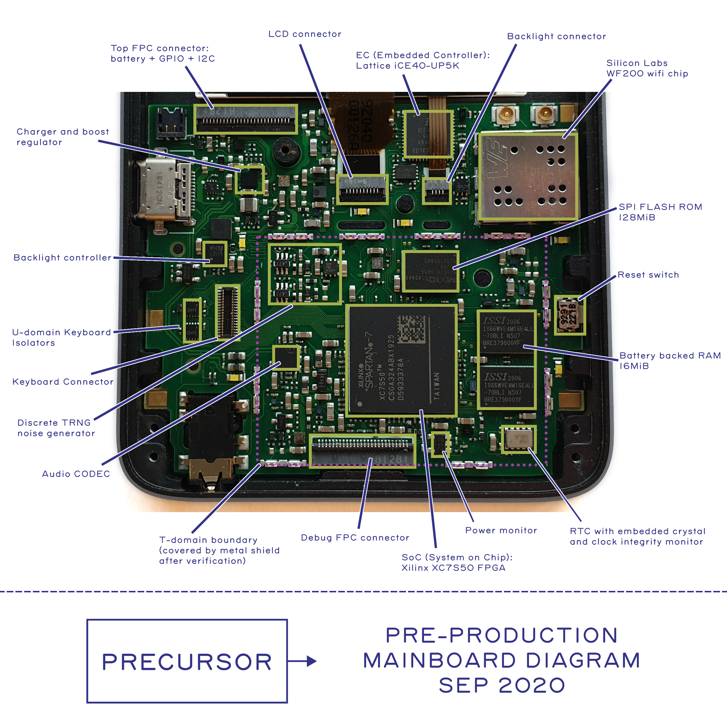
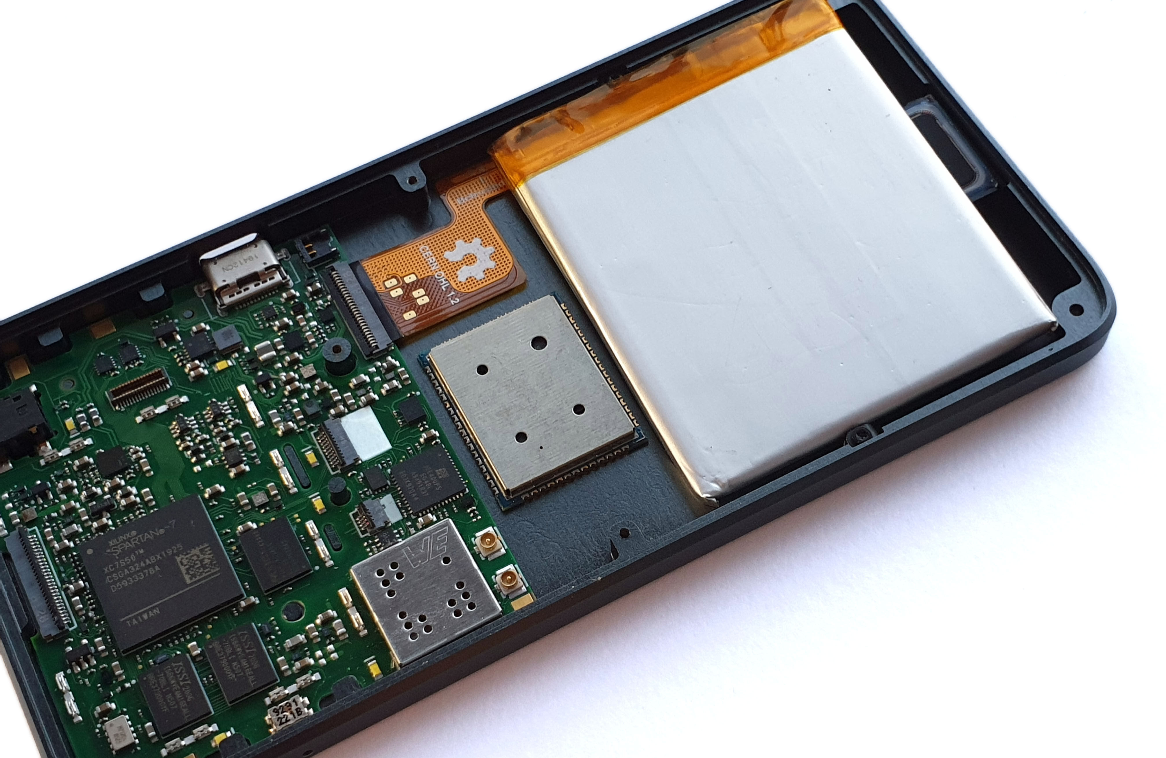
Above is a photo of a pre-production version of Precursor, annotated with the location of key components. Like software, hardware has revisions too. So, when verifying a system, be sure to check the revision of the board first. The final production units will have a clear revision code printed on the back side of every board and we’ll tell you where to look for the code once the location is finalized. There will be a few changes to the board before production, which we’ll talk about later on.
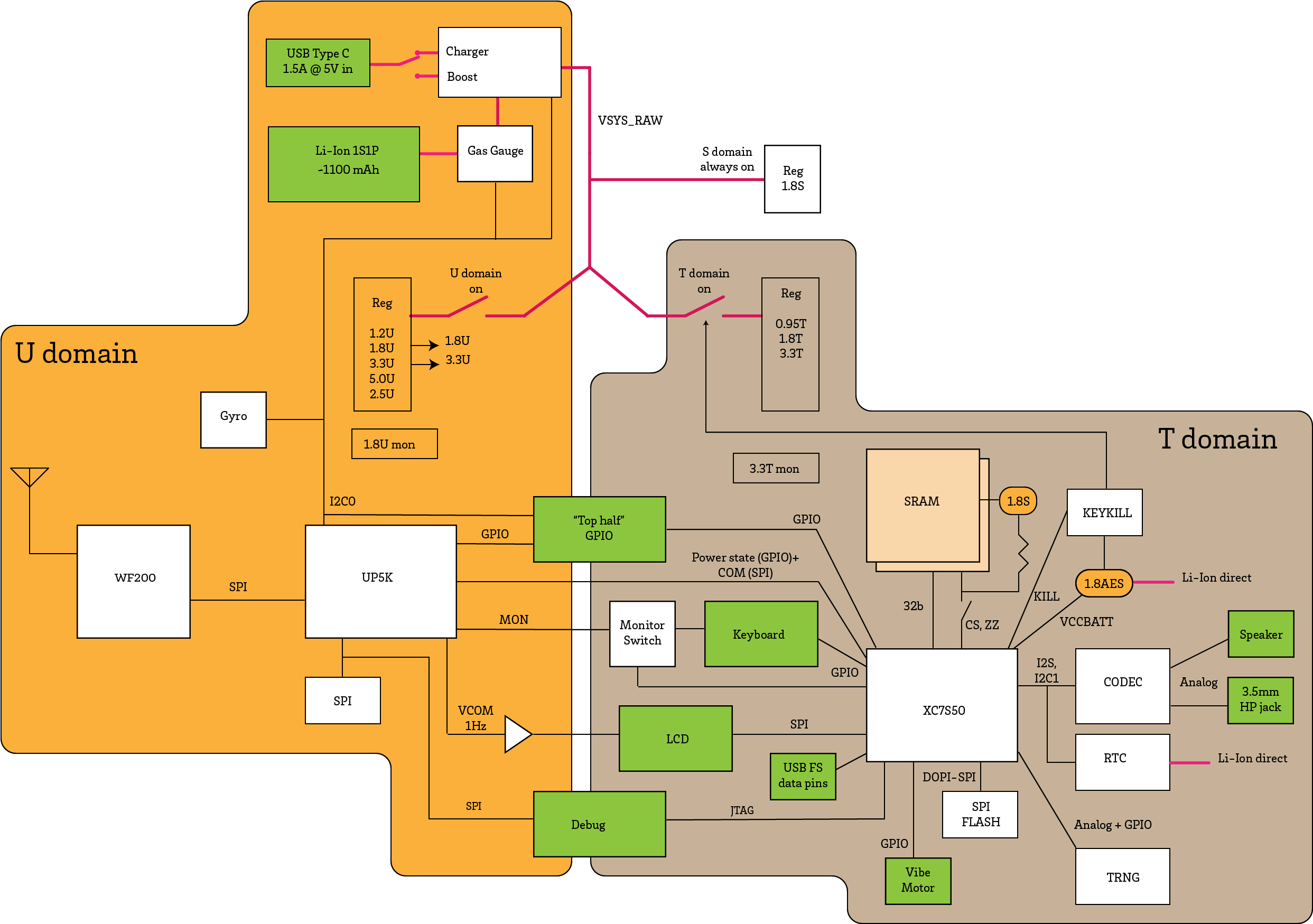
But what do all the components do, and how are they connected? Above is a block diagram that tries to capture the relationship between all the components.
Trusted and Untrusted Domains
First and foremost, you’ll notice that the design is split into two major domains: the “T-domain” and the “U-domain”. “T” stands for “Trusted”; “U” stands for “Untrusted”. A simplified diagram like this helps to analyze the security of the system, as it clearly illustrates what goes into and out of the T-domain; in other words, it defines the hardware attack surface of the trusted domain. Of course, not shown explicitly on the diagram are the side-channels, such as RF emissions and power fluctuations, which can be used to exfiltrate secret data. Very briefly, RF emissions are mitigated by enclosing the entire T-domain in a Faraday cage. Meanwhile, power fluctuations are mitigated partially through local filtering and partially through the use of constant-time algorithms to perform sensitive computations.
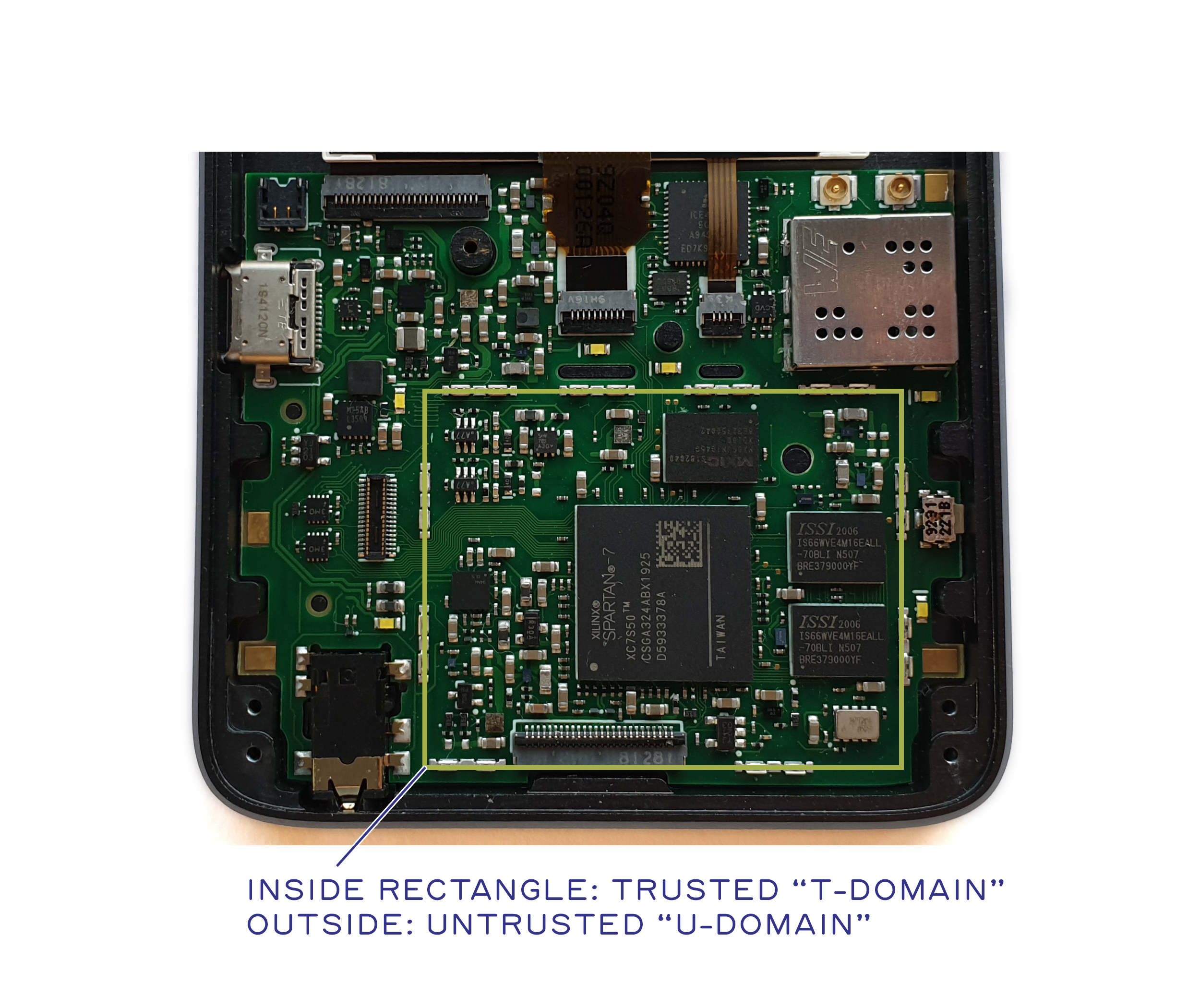
As the “Trusted” name implies, the T-domain is where the secrets go, while the U-domain acts as a first-level firewall to the untrusted Internet. The U-domain is explicitly designed for very low power consumption, so that it can be “always on” while still providing several days of standby time. We refer to the FPGA inside the U domain as the Embedded Controller (EC), and the FPGA inside the T-domain as the System on Chip (SoC) or sometimes simply as “the FPGA”.
Power Management and the Embedded Controller (EC)
The intention is that the always-on EC listens for incoming wifi packets; only once a valid packet is received will the T-domain be powered on.

Using a low-power EC separate from the SoC allows power-hungry processing to be done in bursts, after which the T-domain powers itself off. Thanks to the “memory LCD” that we have chosen, the display can appear persistently even when the T-domain is powered down. Of course, leaving data on the screen while the T-domain is powered down is a potential security risk, but users can adjust the power policy to trade off between security and battery life based on their particular use case and threat scenario. We anticipate that the T-domain running full bore with no power management would exhaust an 1100 mAh battery in about 6-7 hours. Any time spent in an idle state will greatly extend the battery life; thus for a hypothetical messaging application where the CPU is only active during periods of typing and data transfer, one should be able to achieve a full day of use on a single charge.
Mapping the T-Domain Attack Surface
Extending the boundary of trust to include human-facing I/O is a core tenet of the Precursor secure design philosophy. Thus, the T domain also includes the keyboard, LCD, and audio elements. This is because deferring the rendering of messages to an untrusted display means that any cryptography used to secure messages can be trivially defeated by a screen scraper. Delegating keystrokes to an untrusted touch controller likewise offers a quick work-around for capturing outgoing secrets through a keyboard logger. To mitigate/prevent this, Precursor incorporates an LCD that can be verified with an optical microscope and a physical keyboard that is trivial to verify with the naked eye. Precursor also forgoes an integrated microphone and instead favors a 3.5mm headphone jack, thus putting users solidly in control of when the device may or may not have the ability to record a conversation.
The green boxes in the block diagram above are connectors. These are items that plug into components that are not integrated into the mainboard. With this in mind, we can define the attack surface of the T-domain. We can see that we expose GPIO, USB, and JTAG to external connectors. We also have a bus to the U-domain that we call the COM bus, as well as a pair of quasi-static pins to communicate power state information and a set of pins to monitor the keyboard for user wake up events. Let’s explore each of these attack surfaces in a little more detail.
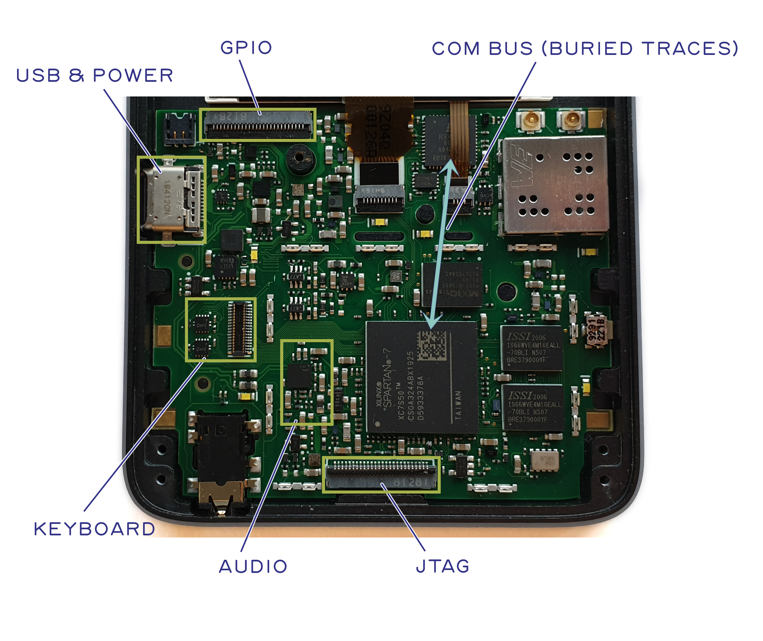
- JTAG A user is required to glue shut the JTAG port when the system needs to be sealed and secrets made inaccessible. This is done by placing a metal shield can over the T-domain and dabbing a specially formulated epoxy into the holes. This simultaneously completes the Faraday cage which reduces side band emissions while making the JTAG port more difficult to access.
- GPIOs and USB In its default configuration, the GPIOs are inert, and thus a difficult attack surface. We also advocate leaving the USB pins disconnected for secure applications; however, developers may opt to wire them up inside the FPGA, at the risk of opening up the expansive USB attack surface.
- Raw Power Input The primary postulated attack surface resulting from the raw power input are glitches. Denial of service is of course also an issue, by removing power or by destroying the system by applying too high a voltage; but these are beyond the scope of this discussion. The primary countermeasure against raw power input glitches is a reset monitor that will extend any glitch into a several-millisecond long reset signal if the voltage drops below a prescribed level. Furthermore, local filtering, regulation and power storage removes very short glitches. All T-domain power signals are routed so they are fully contained within the T-domain shield can. No T-domain power signals are exposed as outer-layer traces or vias on either the top or back side of the PCB outside of the T-domain shield.
- Power State Pins The power state pins allow the EC to coordinate with the FPGA SoC on the current power state. They are structured as “read only” from the SoC, and are also considered to be “advisory”. In other words, the SoC is capable of independently forcing its own power into the on-state; therefore the EC is only able to shut down power to the SoC when it is explicitly allowed by the T-domain. This minimizes the risk of the EC attempting to perform a glitch attack against the SoC by manipulating its access to power.
- Keyboard Wakeup Pins In order for the EC to know when to power on the system, the EC also has access to a pair of row/column pins on the keyboard matrix. This enables the EC to respond to a two-key chord to wake the system from sleep; however, it also means the EC can potentially monitor a few keys on the keyboard, leading to a potential information leakage. This is mitigated by a set of hardware isolation switches which the SoC uses to deny EC access to the keyboard matrix once the system is powered on.
- Audio is rendered by way of a CODEC chip. The DVT prototype shown in the photo above uses the LM49352, but a few months ago it was announced to be end-of-life by the vendor, TI. For production, we plan on employing the TLV320AIC3100, a functionally equivalent CODEC which will hopefully have a longer production lifetime. The CODEC chip integrates all the circuitry necessary to amplify the microphone, drive a pair of headphones, and also drive a small speaker for notifications. While it is possible to bury implants within the audio chip, it’s thought that any implant large enough to either record a useful amount of conversation or to do speech-to-text processing of the conversation would create an easily detectable size or power signature, or both. The headphone jack is wired for optimum compatibility with headsets from the Android ecosystem.
- COM bus Finally, the COM bus is an SPI interface used by the T-domain to talk to the rest of the world. It is directly connected to the EC. The COM bus is structured so that the SoC is the sole controller of the SPI bus; the EC is not able to send data to the SoC unless the SoC allows it. Further packet-level and protocol-level countermeasures are required on the COM bus to harden its attack surface, but at the end of the day, this is the primary pathway for data to reach the T-domain from the outside world, and therefore it should be the primary focus of any software-oriented attack surface analysis.
It is important that COM bus packets be authenticated, encrypted, and serialized prior to hand-off to the EC; the EC can only put T domain data into the appropriate envelopes for routing on the Internet and no more. This allows us to safely delegate to the EC the job of mapping COM bus packets onto a given network interface.
COM Connects to the Internet
Secure software running on the T-domain should be as oblivious as practical as to what type of Internet connection is implemented by the EC. Thus whether the EC routes COM packets to wifi, LTE, bluetooth, or Ethernet should have no bearing on the security of the T-domain.
For Precursor, we have chosen to add a Silicon Labs WF200 wifi chip to the EC as a primary means of Internet connectivity. The Silicon Labs WF200 contains a substantial amount of un-trustable code and circuitry; however, because the WF200 is in the Untrusted domain, we have no need to trust it, just as we have no need to trust the cable modem or the core network routers on the Internet.
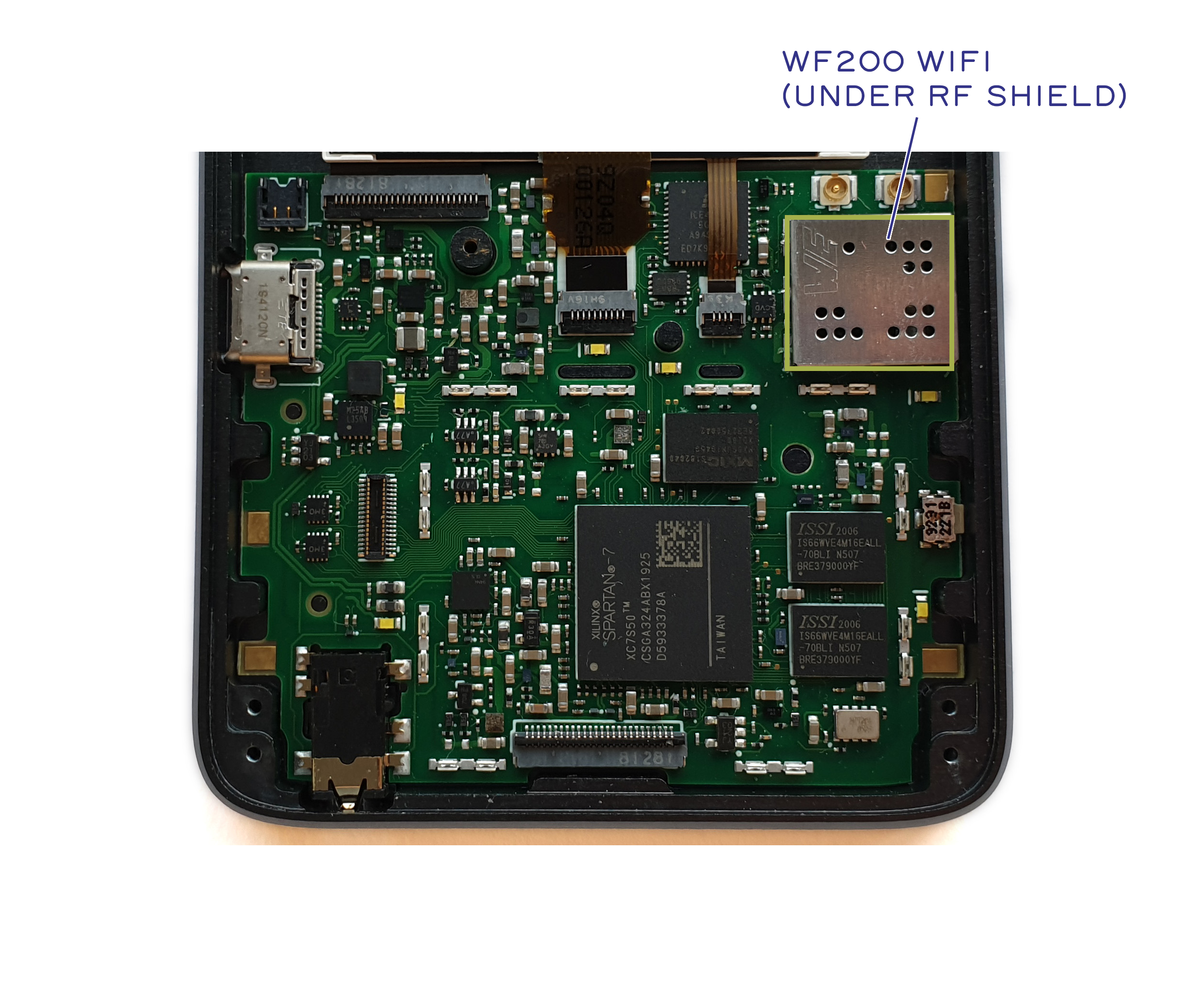
Thus we can safely leverage the substantial co-processing within the WF200 to handle the complications of associating with WAPs, as well as other MAC/PHY-level nuances of wireless Ethernet. This allows us to substantially reduce the power requirements for the system during “screen off” time when it is mainly waiting to receive incoming messages. Furthermore, the WF200 has a well-characterized low power mode which agrees well with bench measurements. This is different from the ESP32, which as of a year ago when the evaluation was done, advertises low power but suffers from power-state transition nuances that prevent a practical system from achieving overall low power consumption.
The EC takes care of uploading firmware to the WF200, as well as servicing its interrupts and transcribing received packets to the T-domain. In addition to these responsibilities, the EC can detect if the system has been physically moved during standby by polling an IMU, and it also manages the battery charger and gas gauge. It also provides a ~1Hz square wave to the LCD that is required by the LCD during standby to continue displaying messages properly.
Random Number Generators
The T-domain includes a discrete TRNG. This is meant to complement a TRNG integrated into the SoC itself. The benefit of a discrete TRNG is that it can be verified using common lab equipment, such as an oscilloscope; the drawback of a discrete TRNG is that an attacker with physical possession of the device could manipulate its output by drilling through the RF shield and dropping a needle onto millimeter-scale component pads.

The integrated TRNG inside the SoC is less vulnerable to attack by a physically present attacker, but at the expense of being difficult to manually verify. Thus, we provision both discrete and integrated TRNGs, and recommend that developers combine their outputs prior to use in secure applications.
Keeping Time
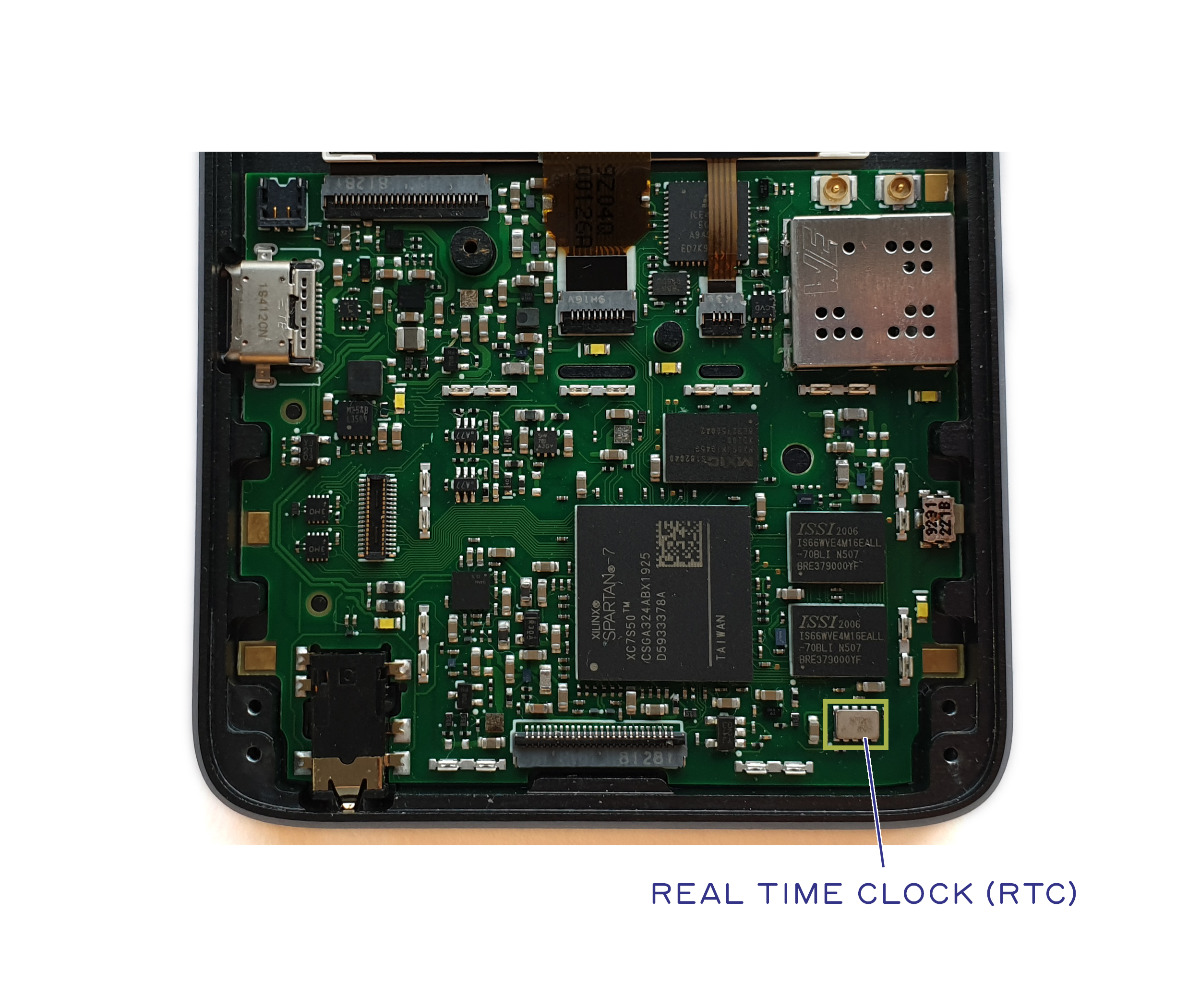
A sense of time is important in many cryptographic protocols, thus a Real Time Clock (RTC) is a security-critical element. We chose an RTC that integrates both the crystal and the clock chip into a single hermetically sealed package to reduce the attack surface available to a physically present attacker to manipulate time. The chosen RTC also incorporates basic clock integrity checking, which helps to mitigate simple glitch attacks against the RTC.
RAM: Why 16MiB?
We provide 16MiB of battery-backed SRAM for secure computations. We made it battery-backed so as to reduce the standby/resume overhead of the system, at the expense of creating a potential attack surface for physically present attackers to recover data from the system.
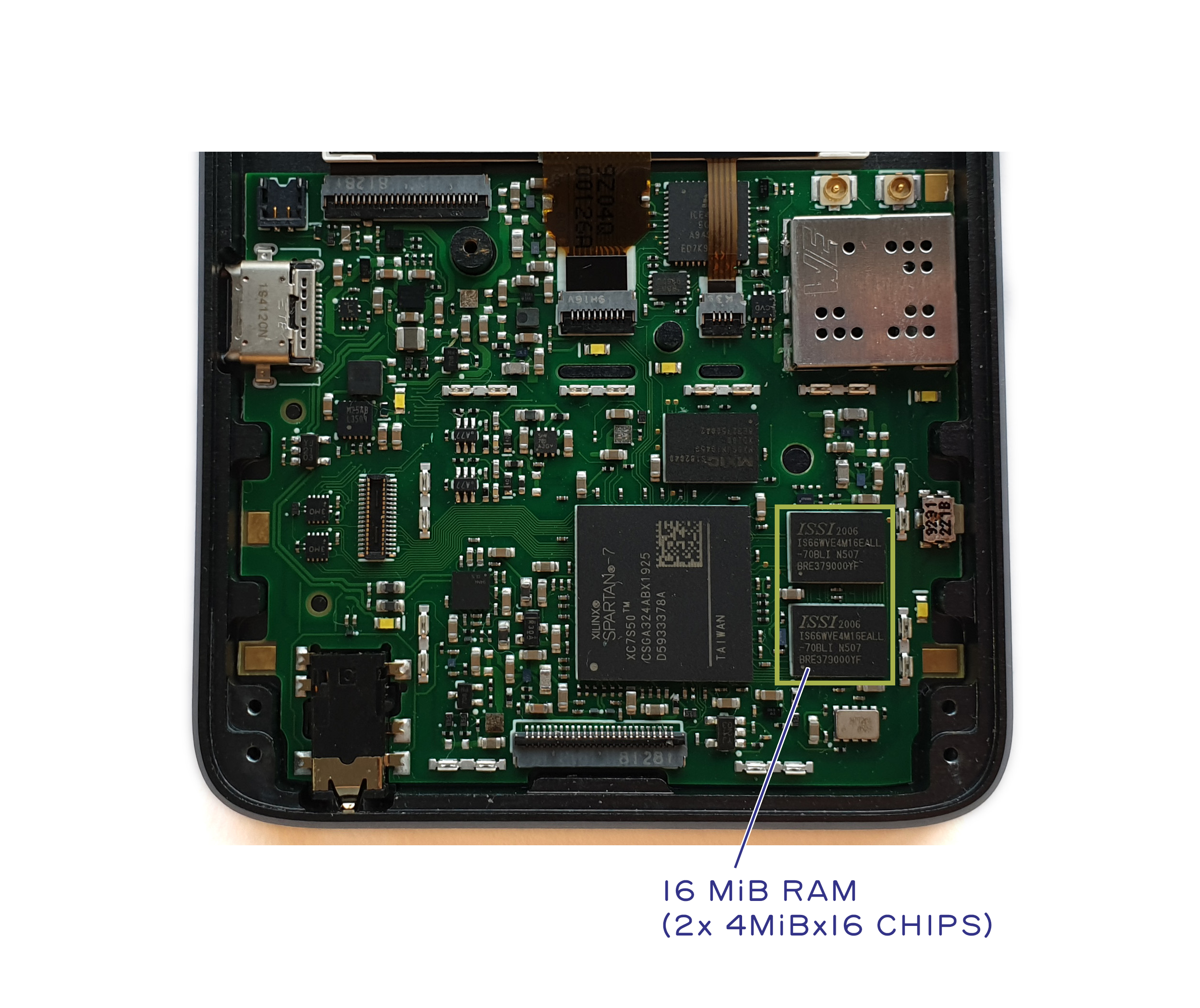
The choice of 16MiB of SRAM was deliberate and motivated by several factors:
- Power A larger DRAM would have required using the DRAM PHY on the SoC. This interface is extremely power hungry and would have more than doubled the amount of power consumed when the system is on. Furthermore, keeping the DRAM in self-refresh mode would disallow powering down the FPGA entirely, meaning that the substantial standby leakage power of the SoC would count against the “screen-off” time.
- Code complexity Precursor is a spin-off from the Betrusted project. One of Betrusted’s goals is to build a codebase that could be audited by an individual or small group within a reasonable amount of time. Choosing a small amount of RAM is the equivalent of burning the boats before a battle to force an advancing army into a win-or-die situation; it confines every choice made in the OS and application layers to prefer simpler, less complex implementations at the expense of more development time and fewer features.
- Roadmap Eventually, we would like to fit the entire T-domain of Precursor into the footprint of a single chip. Incorporating hundreds of megabytes of RAM on-chip is impractical, even in aggressive process nodes. In a more realistic 28 or 40nm node, we estimate 4-16MiB is a potentially practical amount of RAM to incorporate in a low-cost, low-power, mass-market implementation. Provisioning Precursor with a similar amount of RAM helps to ensure code developed for it will have a migration path to more highly integrated solutions down the road.
Self-Destruct Mode
Finally, we have provisioned a “self-destruct” feature for users that opt to use battery-backed AES keys to protect their FPGA image. The “self-destruct” mechanism consists of a latch built using discrete transistors. During normal power-on, the system latches into a “normal” mode of operation. However, when the SoC asserts the “KEY_KILL” pin, the latch switches into the “kill” mode of operation. Once in the “kill” mode, power is cut to the T-domain – including the power that backs up the AES key. There is also a set active pull-downs which rapidly discharge the relevant voltage rails to ensure the power lines drop to a level suitable for data erasure in a matter of milliseconds. Although the data erasure only takes a fraction of a second, the only way to get out of “kill” mode is to remove the battery or to wait for the battery to fully discharge.
That wraps up our whirlwind tour of the Precursor motherboard. This post introduced all of the major design features of the Precursor motherboard and briefly summarized the rationale for each choice. The system architecture minimizes the attack surface of trusted components. Furthermore, component choice was guided by the principles of simplicity and transparency while trying to provide a complete but auditable solution for security-sensitive applications. Finally, the mainboard was designed with components only on one side, and all security-critical components are contained within a well defined area, with the hope that this makes it easier to visually inspect and verify units upon receipt by end users.
Liked this post? Sign up to the Precursor funding campaign mailing list to be notified when new posts go live!