Archive for the ‘Hacking’ Category

Winners of Name that Ware May 2006!

Wednesday, July 19th, 2006

Well, it’s been a long June. Actually, it’s been a very interesting past couple of months; some of the most interesting stuff will appear on this blog in late August, but for now I have to keep quiet about some of the things that have been keeping me busy. I’ll drop one hint, though–I’m working on a project that has an open source hardware aspect, and I am looking forward to sharing the details with everyone once things are rolling. I’ve always felt that hardware should ship with schematics and source code, and I finally have a chance to make good on this notion. I also did a bit of the conference circuit this past month, with a talk at Recon 2006 in Montreal and the National Youth Leadership Forum on Technology in San Jose.

I apologize for missing June’s name that ware; to make up for it, the next name that ware contest will have two wares. I actually had a ware all queued up and ready to go, but the combination of an exciting July 4th holiday and tons of travel for the past couple of weeks, as well as a deluge of spam on the blog, has kept me away from posting. If anyone posted a comment in the past month, there’s a very good chance I accidentally marked it as spam, because as I mention in the previous post I was getting upwards of 50 spam posts a day. The upgraded blog software and spam filter seems to have fixed this problem, thankfully.
For May, 2006, we have a number of winners! I’m glad that so many people participated in the contest. jimmyjo, roastbeef, and christian all win prizes this month (email me to pick your prize and I’ll send it on to you!). jimmyjo and roastbeef both got an easy and medium ware correctly. Christian went all the way and jumped headlong into one of the hard ones!

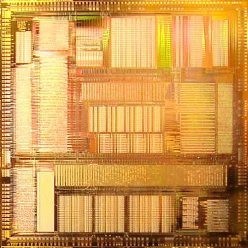
Honestly, when I selected the hard wares, I had no idea if I could figure out what they were, or if they were even do-able, but I wanted to put something up that wasn’t as simple as an inverter. It turns out that they are indeed quite difficult to decipher, partially because M2 blocks some key devices, and partially because the area photographed is not large enough.

While I am not 100% sure of any of my own solutions, I can talk y’all through what I think they are and why. Hard(3) is most likely a simple D-latch or flip flop. The cluster of transistors on the right side, underneath the crosshairs, form a pair of cross-coupled inverters. The cross-coupled inverter motif is the core of any static memory cell, such as those used in a flip flop. Hard(2) turns out to be un-doable, I think, because there is too much M2 running over it: there is a large inverter to the left of the crosshair, and then the logic gets a little more exciting to the right but I gave up.

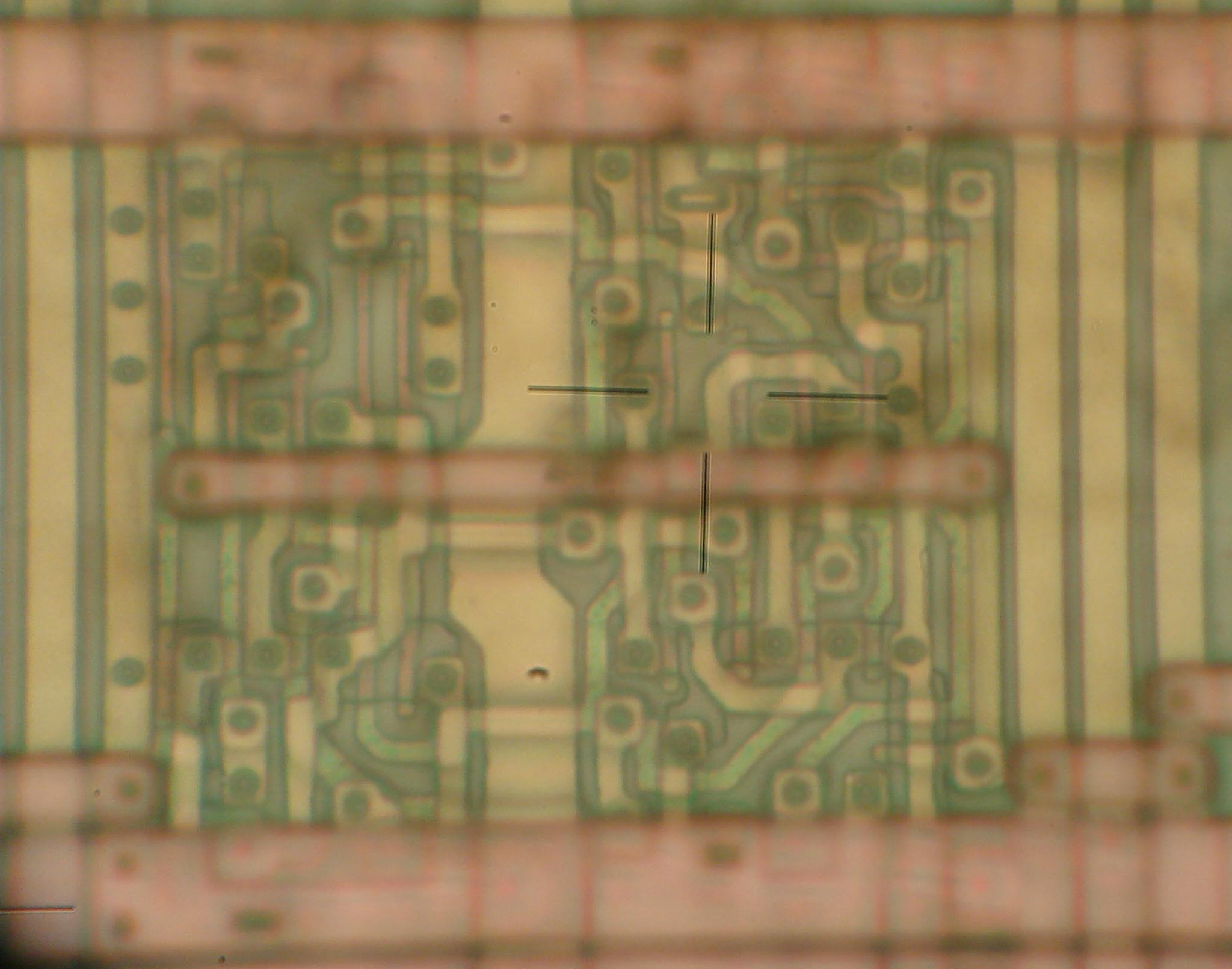
Hard(1) I spent some more time on, because Christian did so much analysis I had to do my homework too to match his efforts. Click the image below.

There are approximately 15 p-type and 15 n-type transistors in this CMOS circuit. As you can see, there is some action happening underneath the M2 power straps that obscures the total function of this cell–I have interpolated some devices and connectivity through symmetry arguments. Also, the huge strap of M1 going through the middle of the cell seems indicative of some kind of clock or strobe-type of signal. The partial schematic on the right helps reveal some of the internal structure. P8-P11 and N8-N11 form some type of cross-coupled inverter pair. If the chain of P9-P11 and the chain of N9-N11 are all activated at once, you can see that (P9-P11/N9-N11) and P8/N8 form a cross-coupled inverter structure. When I first started decoding the circuit, I thought for sure this would be a sense amplifier, but there are some fancy things going on, that look related to controlling set/reset possibly, or perhaps rolling in some additional logic to the storage process as an optimization. If I were to guess as to what this is, it’s some type of flip-flop, I think, but with some extra logic rolled into it for fancy set/reset, muxing or J/K style controls. I suppose if I poked at this some more I could figure out more, but I want to post this and get next month’s wares up! :-)

Hint for Name that Ware May 2006

Thursday, June 8th, 2006

Already, we have correct answers (and winners!) for Name that Ware May 2006, which is really excellent! In order to help people with the more difficult ones, I am posting here an “answer key” for the “medium” ware.

This device is an inverter. The power is on the bottom of the image, and ground is on the top. As mentioned before, you can tell which side is power or ground because the PMOS transistors are larger (due to the inherent reduced mobility of holes, and therefore reduced saturation current per unit width, when compared to electrons). In a static CMOS circuit topology, the PMOS devices typically connect between power and the input/outputs; NMOS devices respectively go to ground.

This particular inverter is laid out as three NMOS and three PMOS transistors slaved together. This multiplies the current drive of the device by three. The reasons for putting devices in parallel instead of making them larger is many-fold. One big reason is that a standard “height” is used for all logic gates and flip flops in a design like this. If a device’s design calls for a gate width that violates the height rule, it has to be broken up into multiple parallel devices. Using a standard height enables automated place-and-route tools to easily drop logic cells side by side, like the movable type on an old-style printing press. Also, parallel devices have lower parasitics for certain key parameters (such as gate resistance), although at this technology node gate resistance probably is not a huge concern. It also occurred to me that it’s possible there is a fourth finger to the left on this circuit (computer people love powers of 2!), and it may just be hidden by the strap of metal 2 running on the left hand side.

You can also download the Visio file that I created to generate this answer key. The Visio file is useful in case you want to take one of the “hard” images and paste them into a new Visio file and use my color scheme as a template. Drawing simple polygons and text notes over an imported .JPG in Visio is a relatively easy way to do bookkeeping on what polygon goes where when trying to decode more complicated circuits.

Good luck, and hopefully people will find this an interesting challenge!

Name that Ware May 2006

Tuesday, May 30th, 2006

The Ware for May, 2006 is a little bit different. This time, I’ll tell you what the ware is, but your challenge is to tell me what specific components do.

This month’s ware is the SGI “PG” chip from the original Reality Engine graphics supercomputer from back in oh…1992-ish. I believe this chip was responsible for polygon generation, hence the acronym PG (I could be wrong, anything over a decade old–heck, a day old–in my brain is liable for bit-rot). I got these chip samples when I used to work for SGI many moons ago, back on their follow-on product to the RealityEngine2 (before it got canned and all the key employees went their separate ways to start or to work at these crazy companies called nVidia, ATI, and 3dfx, all trying to bring graphics to the desktop. Actually, it was this first-hand observation of people movement correlated to the subsequent decline of SGI and the rise of the new graphics companies that convinced me that people are the most important asset of a company, and that individuals can and do matter, even in big organizations).

Since I have silicon on the hacking brain this month, I figured it might be fun to try and challenge readers with some wares that you just can’t look up in google to get the right answer. For first-time silicon hackers, I have a short tutorial on how to read chips.

There are three categories for the ware, just in case it is too easy or too challenging for people. I have one easy ware, one medium ware, and three “hard” wares. I am able to identify the easy and the medium ware with direct visual inspection (hint: they are fundamental logic gates). The three hard wares I suspect what their function is, but I would have to spend some time with a pencil and paper to trace out the circuitry and then try to deduce their precise functions based on the circuit diagram (and it’s quite possible that I couldn’t figure out what they do even after that). Of course, you are operating without the benefit of being able to infer function from the larger context of the overall chip, but the good news is that this is a very old-fashioned 2-layer metal design so almost all the transistors are visible in these photos. I will give out multiple prizes, one for each of these wares, and you can win multiple times (check the rules for the prize possibilities!). So with no further ado:

Easy (left)         Medium (right)
 

Hard (1)

Hard (2)

Hard (3)

good luck, feel free to discuss and ask questions…I will help with hints if people need them.

Winner of Name that Ware April 2006!

Tuesday, May 30th, 2006

Again, people aced this ware left and right. tmbinc somehow managed to post a near-instantaneous response that was 100% correct, but since he won last time, I decided to give someone else a chance. So, Julian Calaby, you are the winner of Name that Ware April 2006, since you got both answers correct in the same post, and you had a fair bit of analysis too! Thanks for playing. email me to claim your prize (and if I’m not mistaken, I still owe tmbinc a prize, too). Unfortunately, aqua, I could not generate a hash collision for your answer, so to this point I don’t know what it is!

The correct answer for the two wares is a Nokia 770 for “ware 1” and a GP2X for “ware 2”. I was surprised at how quickly people got the Nokia 770, since I figured it was a bit more obscure than the GP2X. I’m always impressed at the extreme level of engineering that goes into these portable products–it’s hard enough for me to get my screw holes to line up on my boards to the stand-offs in the case, and yet these guys manage to some how Tetris these devices into complex 3-D housings and it all snaps together beautifully. It’s always a great learning experience taking these apart and observing the techniques and component choices that good engineers use in making these products.

A Note about the Xbox360

Tuesday, May 30th, 2006

There is a WSJ article that was printed today that reports on some of my (relatively insignificant) dabblings on the Xbox360. I have kept a very low profile with respect to working on the Xbox360, but I guess this article changes things. The article is reasonably accurate, but I feel the need to clarify a few things.

First, hacking the 360 is not a race between me and The Specialist; the “bunnie v. Specialist” tag line is a result of the WSJ’s editorial latitude and their perspective on the scene (and I, of all people, must respect their first amendment rights to report as they see fit, seeing as how I also stand behind the first amendment to protect my right to blog about controversial hacking topics). I give The Specialist huge props for his DVD firmware hack; it’s a great hack and I respect his work a lot. When we found out about his work we were very excited and appreciated the great contributions he’s made in furthering an understanding of the overall security system of the 360. We wouldn’t be anywhere near where we are today without the openness and information-sharing that pervades the hacking scene, and I hope that the portrayal of hacking as a competitive sport does not close off these avenues. I know that I would not be where I am today if it were not for the great collaborations I’ve had in the past with so many anonymous hackers, and my ability to contribute on the 360 would also be greatly diminished if I were to lose such valuable collaborations.

Second, while I have been dabbling in the Xbox360, I’ve been a bit delinquent lately–very busy with my day job, and I haven’t touched the Xbox360 to do any real work on it for a couple months. I owe Speedy22 an apology for not being more diligent about sending him micrographs of the XCPU, but really, right now the pictures aren’t very interesting because all the metal is still on the chip (working with a local vendor to get it removed but it takes a lot of time). Speedy22 was kind enough to provide me some samples of the Xbox360’s chips to digest, and I appreciate his generosity in sending them to me. I also owe tmbinc an apology, I was supposed to run a set of experiments on the “virgin” ROM images that I never got around to. If you still need those results, I’ll get to it.

In the meantime, I hope to refine a technique that will gain access to the polysilicon layer of the XCPU while being non-destructive to the function of the chip. Such access is currently thought to be a major stumbling block to extracting the necessary keys for decrypting firmware images on the Xbox360–and the first step toward homebrewing code on the Xbox360. I wouldn’t hold my breath, however–the technique is very risky and I don’t have a whole lot of time to perfect it. I have to build some custom equipment to help control the etch bath properties for peeling back the silicon. Still, it will be fun and even if it is not successful, I’ll learn something new while I develop the hack!

(above) Micrograph of the logo region on the 360 XCPU die. The pattern of metal dots you see are the fill pattern used to make the metal layers statistically uniform at the macro-level for the purposes of chemical-mechanical polishing (CMP), a process used to planarize metal layers during manufacturing. CMP is an important enabling technology for both copper technology (dual-damascene processing) as well as for enabling very high metal-layer counts to meet the wiring demands of today’s technology. Before CMP technology, metal layers would develop a 3-D topography that would limit the height of metal stacks. As one can see, CMP tiles also make a great tamper-resistance measure because the CMP tiles interfere with reading the underlying silicon patterns. Peeling back these layers is a destructive process, and can be a difficult and time-consuming. It requires a similar chemical-etch and mechanical-polish technique used during fabrication, and the technique has to be precise to sub-micron depths across a relatively large area. Alternative techniques are being developed to solve this problem.