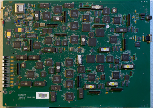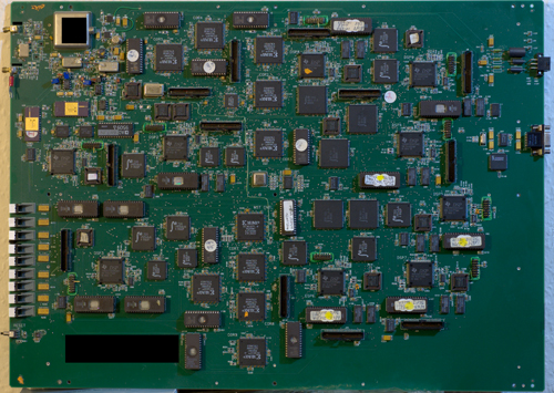
Congrats to Adam Gutterman for finding the cake. The cake is hidden on an internal ground layer, printed in “negative” (i.e., lack of copper on a copper plane). The visible-light photos I make of the motherboards are all taken with front-lit scanners, so the negative image is virtually invisible when viewed in that way. There’s also a solid copper ground plane behind the cake as well, so you can’t simply hold the board up to a light to find the cake (hence the larger bounty). The only two methods to find the cake are to either X-ray the board, or to mechanically delaminate the board using either knife or sandpaper (or both) to reveal the cake. And for the record, the region where the cake is located is electrically inert, such that defacing the chumby logo to reveal the cake does not damage the function of the device.
Adam tells the story of how he found the cake:
I’m an EE at a company that outsources almost all of our board assembly tasks. Anything more complicated than QFPs gets sent out–it’s not worth engineer time to assemble things, especially since we’re not particularly skilled assemblers.
Unfortunately, not all projects have the budget for professional installation. During a recent personal project, we hand-assembled a small batch of boards that had pretty tiny LGA packages. Our initial yields were pathetically low, and we suspected that there were some shorts to blame. Since we didn’t have a professional lab to use, we had to go with our personal connections. The board designer found a friend that had access to a medical x-ray machine, so we sweet-talked ourselves into a quick run through their machine. The resulting film let us get over our hump and bring our boards up successfully.
Anyway, as soon as I saw your post, I decided to do the same thing. Unfortunately, the x-ray office was closed for the long weekend, so I wasn’t able to get my ‘stat’ order in until Monday. When I got the films last night, the focus wasn’t clear enough for me to be able to make out any important features. The films, incidentally, are shown in the directory that I posted on your blog. Undeterred, I spent last night trying to get permission to use a PCB inspection facility at a local university. The okay came through this morning, so during lunch today a couple of us set the board up and started looking for features. It took only a couple of minutes to find the cake once we had access to the right equipment!
I didn’t think it would be found so quickly…just one week from original post, for an item that’s entirely concealed on an inner layer. Then again, ladyada got her open-source Kinect drivers in about the same period of time.
This is probably an interesting datapoint for folks who support the theory that burying traces on the inside of a PCB are an effective method for obscuring the transmission of secret information between chips.


