Archive for the ‘Hacking’ Category

Winner, Name that Ware March 2010

Saturday, May 1st, 2010

The Ware for March 2010 was an N1100 Roku HD player. Matt Burkhard was the first person to correctly guess the model number, so congrats! Thanks for playing, and email me to claim your prize.

The chip with the epoxy around it is an HDMI PHY. I found it sort of amusing that the manufacturer went through the trouble of pouring epoxy over the pins of the chip…

Very tight on time this month, got delayed in Europe for a week due to Eyjafjallajökull and still digging myself out from under the backlog, so the commentary for this months judging and ware are a bit brief.

Make Your Own 3G Router

Thursday, April 29th, 2010

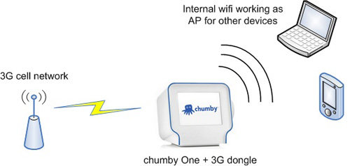
There’s an Easter Egg inside the chumby One (which is now on sale at Costco online for $99, cheaper than chumby.com’s $119 price!) that enables it to work with certain 3G USB modems and function as a 3G router (similar to a MiFi).

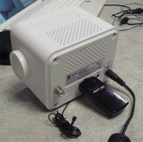
Above is a picture of a Verizon USB760 modem plugged into the USB port of a chumby One.

Use of the Easter Egg is documented on the chumby wiki, but it can be quite simple:

1. Plug in your 3G card.
2. Go to the Network Config screen by pressing the top button, going to Settings, then tapping on Network.
3. Select “create a new connection”, press OK, and wait for the scan to time out.
4. Select “Other”
5. Enter 3G as the name of the access point. It must have a capital G for it to work.
6. Wait for the subsequent scan to time out.
7. Select “Manual”.
8. Tap “OK” to select None as the encryption type.
9. Tap “OK” to select Automatic IP allocation.
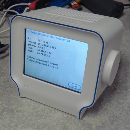
10. Tap “OK” to confirm settings and connect to the network

To activate local wifi sharing, ssh into the device (or plug in a USB keyboard to activate the drop-down console) and use the command “touch /psp/start_ap” to flag the network setup scripts to configure your chumby One as an access point. Note that AP mode also works with other network sources, such as Ethernet-over-USB.

This works because the chumby One ships with a copy of pppd, hostapd and a set of glue scripts (courtesy of xobs) that allow it first to talk to the 3G network, and second to work as an access point that shares the 3G connection with other wifi devices using its internal wifi card.

Since this is an Easter Egg, it has a few rough edges on it, such as no native UI to do things like configure your AP SSID and encryption mode, and for many GSM networks you’ll need to enter a custom username, password and phone number; but you certainly can ssh in and tweak the scripts to set those things up. Regardless, this is a very handy trick that I’ve used in hotels from Shenzhen to Tokyo to New York to set up a wifi hotspot (complete with Internet radio and chumby apps) on the road — the hack works with quite a few 3G dongles and networks (given a little tweaking).

iFixit: knowledge empowers us to recycle

Tuesday, April 27th, 2010

I thought this was a great video; love what Kyle is doing at iFixit. I had heard about the e-waste farms in Africa but never seen footage of them, until now.

Something to think about.

Name that Ware, March 2010

Monday, March 29th, 2010

The Ware for March 2010 is shown below. Click on the photos for a much larger version.

Thanks to Google, this ware may be fairly trivial to guess, but in a feeble attempt at heightening the challenge a tad, I cropped the main connector bank on the PCB, blurred out the CPU’s part number (just a little), and will give bonus points for naming the exact model number of the Ware.

…is that epoxy I see around an IC? I wonder why that is there. ;-)

Winner, Name That Ware February 2010

Monday, March 29th, 2010

The Ware for February 2010 is, to the best that I can tell, a variant of the HTC Touch Dual. Since this was an unknown ware for me, judging the winner is always very hard. Based on the link David Gabler sent (congrats on winning, email me for your prize!), I eventually landed at a page of mobile phone service manuals by Mike Channon, of which there is a link to the Touch Dual repair manual, e.g. the “Nike Series Mother Board Repair Guide” (the page asks not to link directly to any of the PDFs, so I’ll respect that and you’ll have to search for “Touch Dual” yourself).

The board outlines and connectors are at roughly the same places, but there are some significant differences in the position of ICs on the side with the SIM card connector. These different ICs are all related to the RF portion of the design, so quite possibly it’s a situation where the variant of the HTC Touch Dual motherboard shown for this ware simply has a different RF section in it from the one in the service manual. There’s a lot of good reasons for that variance — simply being able to work with different networks in different countries may necessitate a significant change to the RF section.

Addressing some of the comments in the ware discussion thread, the board is indeed using blind/buried vias, so with enough layers essentially the board designer gets the luxury of treating each side of the PCB as if they were two separate layouts. As a byproduct, you get the flexibility to pull off a feat such as swapping out all the components on one side of the PCB without affecting the layout on the other side. If a traditional through-hole board technology were used, this would be a nearly unthinkable option. This is a neat trick to see realized in a volume product, and one I will keep in my pocket for use at a later date.