The Ware for March 2025 is part of a Wekome WP-U157 “67 watt” GAN power supply.
This particular unit had overheated and let out the magic smoke, so I decided to take it apart to understand what was going on. There were a number of engineering issues with the design; the most prominent of which is that the gap filler pads used to improve thermal conductivity had settled, and were no longer making intimate contact with the case. The small air gap meant the electronics were effectively cooking in a thermos.
I think Kienan basically nailed it (congrats & email me for your prize) – as with most Chinese products, the make/model number is just a throw-away layer of “business paint” and I suspect the actual OEM for a whole series of similar modules is Shenzhen Goodwin. As indicated by Kienan, the safety margins of this product are inadequate. I had picked up a couple of ~\$90 GaN chargers previously and was quite happy with them; this charger was available in Hua Qiang Bei for about \$30, so I decided to give it a try. It works, for small values of “work” — if you run it at anywhere near the rated capacity for more than a half hour, it’ll eventually shut itself down, presumably due to overheating.
I could believe it has no explicit thermal protection, and instead, perhaps they were relying upon the built-in thermal shut-offs of the regulator ICs to prevent damage. Why waste money on two safety mechanisms when you already have one? This is reminiscent of a “hint” I once saw about implementing battery cutoffs for shipping and long-term inventory storage…instead of adding an explicit FET to cut off a lithium battery to reduce leakage current during inventory storage, “here’s one weird trick” you can use … force the battery into overcurrent protection mode by shorting it before shipping the product. This effectively causes the battery to disconnect, minimizing leakage during transportation; the cutoff resets when you plug the device in and try to charge it, thus allowing you to save the cost of the cut-off transistor. Another motif I’ve seen is “just charge your batteries with a bad 5 volt supply and let the overvoltage protection on the battery act as your regulator”. Clever ideas, in a way, but still: shenanigans.
The charger itself contains three circuit boards. One is a high voltage backplane, that also serves as a heat sink. Line voltage enters this board and is routed through a bridge rectifier plus some filter/PFC caps. Then, there is a module that has the actual GaN device (Meraki MK2789CDG) which goes from the rectified AC line voltage down to 20V DC @ 3.25A, achieving an efficiency of about 93%. At 65 watts, that means about 4.9 watts of heat is generated by this stage alone (not counting the upstream bridge rectifier and subsequent down-regulators), which is already a lot of heat for a small volume without forced air cooling – more than a Raspberry Pi 4. Most of the internal volume of the power supply is filled with the isolation transformer integral to this circuit.

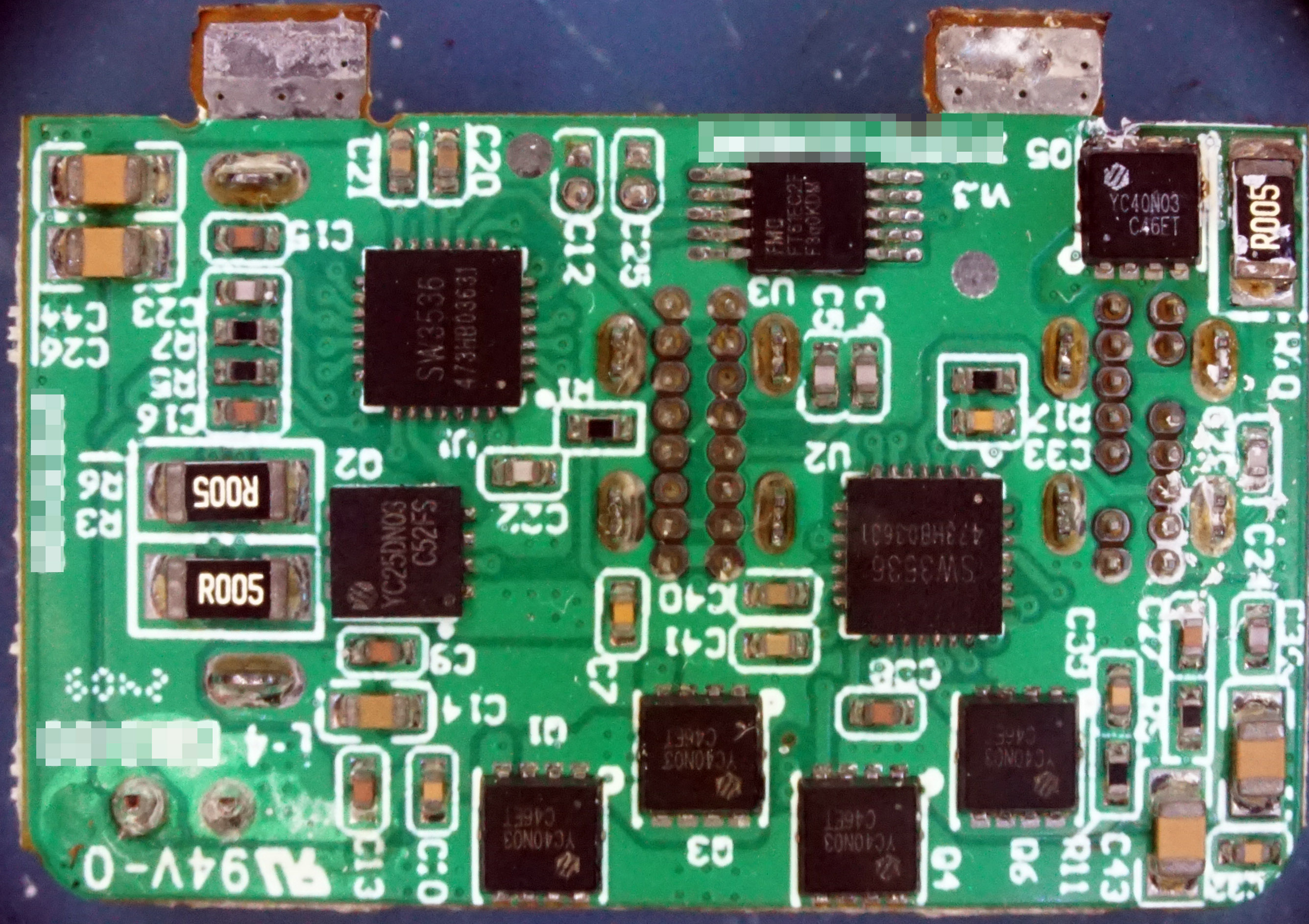
After the AC-to-20V DC stage, there is a set of conventional silicon DC-DC buck converters, which is the board shown as the ware for last month and repeated above for your convenience. The board is parallel to the “face plate” of the power adapter, so space is at a premium. It takes in the 20V from the tabs shown at the top of the image, senses the USB-C PD mode and multiplexes/regulates power to the three ports (2x USB-C and 1x USB-A). This adds additional losses to the supply, but in USB-C 20V PD mode, I would imagine the sync-buck FETs should be operating in a pass-through mode, so there would be no switching losses and you just have the resistance of the (in this case always-on) sync-buck FET + in-line inductors.
Oddly enough, most of the heat seemed to be coming from the face plate of the supply, and not the sides, so something wasn’t working right. I didn’t try to test it after cracking the whole thing apart, but my best theory is that maybe because the gap pads had failed, heat from the GaN core was only really able to escape through this regulator board. The resistance of the transistor and inductor both have positive temperature coefficients, which maybe combined with a lack of an explicit thermal shutdown could lead to a thermal run-away situation where the devices eventually burned themselves out. Datasheets on the YC-series FETs would have been enlightening, but I strongly suspect they don’t achieve the 2 milli-ohm rating hinted at by the sole hit returned by an internet search.