The ware for January 2025 is shown below.
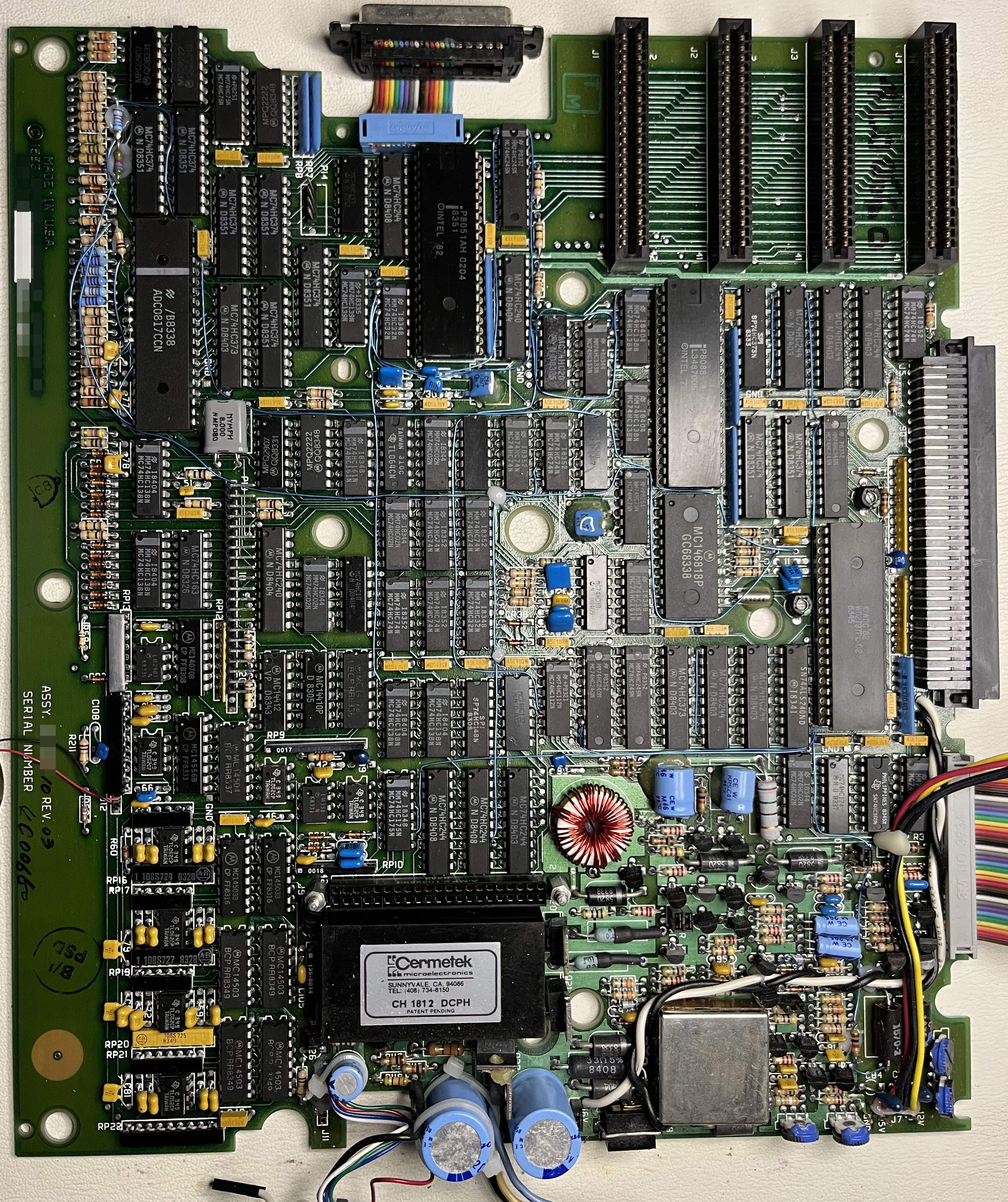
Thanks to brimdavis for contributing this ware! …back in the day when you would get wares that had “blue wires” in them…
One thing I wonder about this ware is…where are the ROMs? Perhaps I’ll find out soon!
Happy year of the snake!
Update Feb 12 2025
Seems to be a stumper. Lots of good analysis, but …
There’s been some mention about seeing the back side of the board; brimdavis was kind enough to provide a nice image of that:
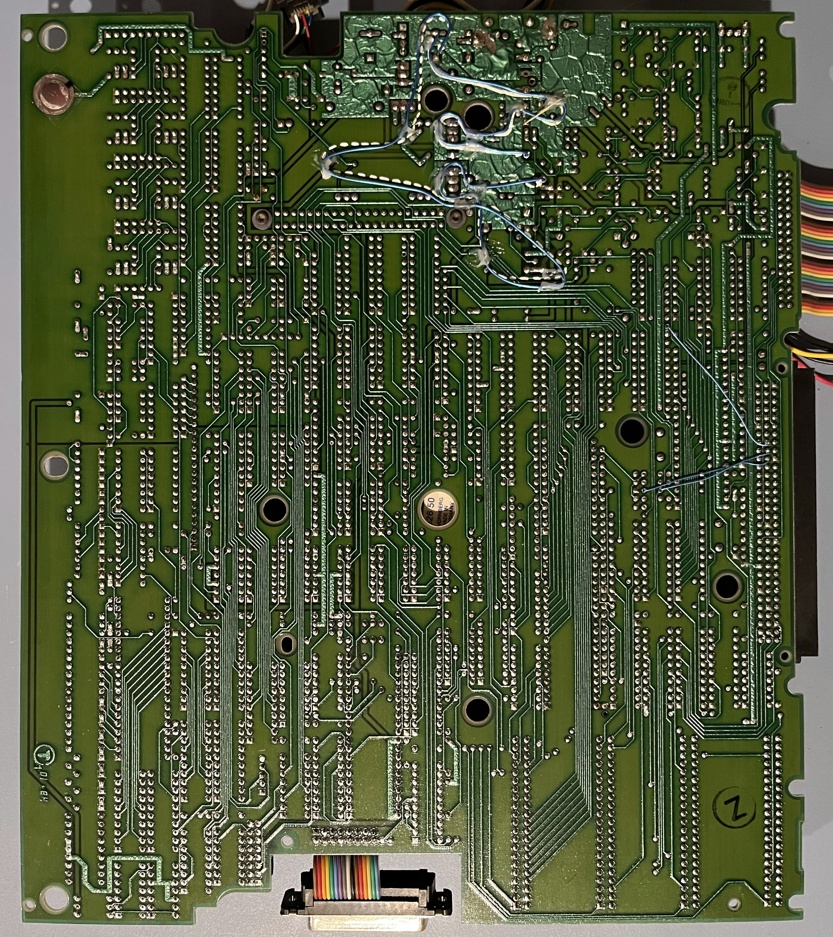
I like how there is a dashed white line for where a blue wire should go.
Also, apparently the “wrinkly” effect is due to a problem “back in the day” where solder wicks under the solder mask during wave soldering? I never got a definitive answer on what causes that, or why modern boards don’t seem to have that issue anymore. In case nobody can guess what this ware is, I’d accept a convincing answer for the wrinkly soldermask mystery as a “tie breaker”.
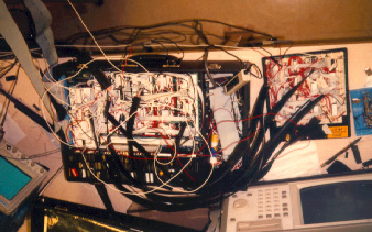
I’ll drop another hint – brimdavis sent me a contextual photo of the assembly, and the ROM, RAM, and video board plug in through the 42-pin connector just above the telephone line connection unit.