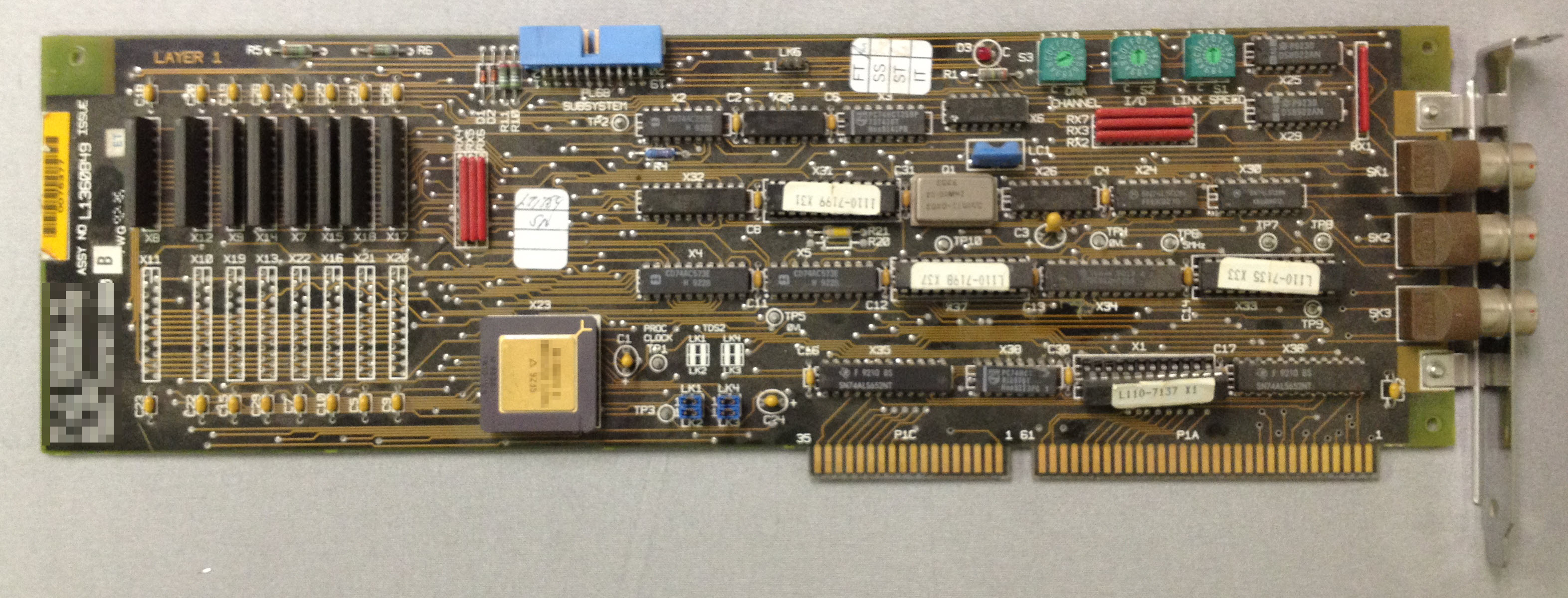
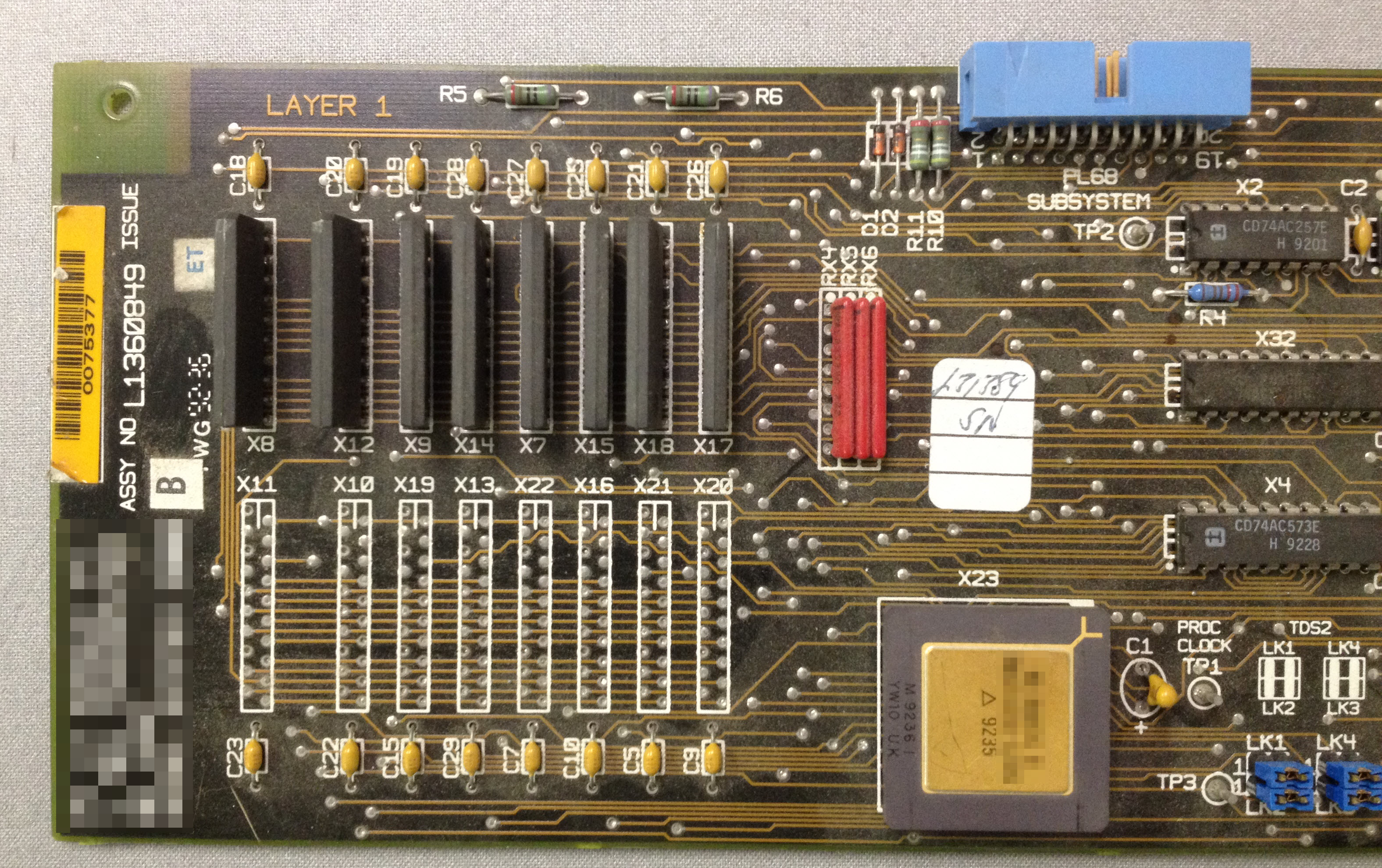
The following is an excerpt from a recent Novena backer update that just got published. I thought the tech bits, at least, might be interesting to a broader audience so I’m republishing them here:
With mainline laptop production finally humming along, bunnie was able to spend a week in Portland, Oregon working side by side with Kurt Mottweiler to hammer out all of the final open issues on the Heirloom devices.
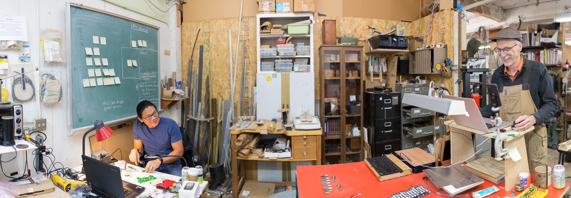
We’re very excited about and proud of the way the Heirloom laptops are coming together. In a literal sense, Heirloom laptops are “grown” – important structural elements come from trees. While we could have taken the easy route and made every laptop identical, we felt it would be much more apropos of a bespoke product to make each one unique by picking the finest woods and matching their finish and color in a tasteful fashion. As a result, no two Heirloom laptops will look the same; each will be beautiful in its own unique way.
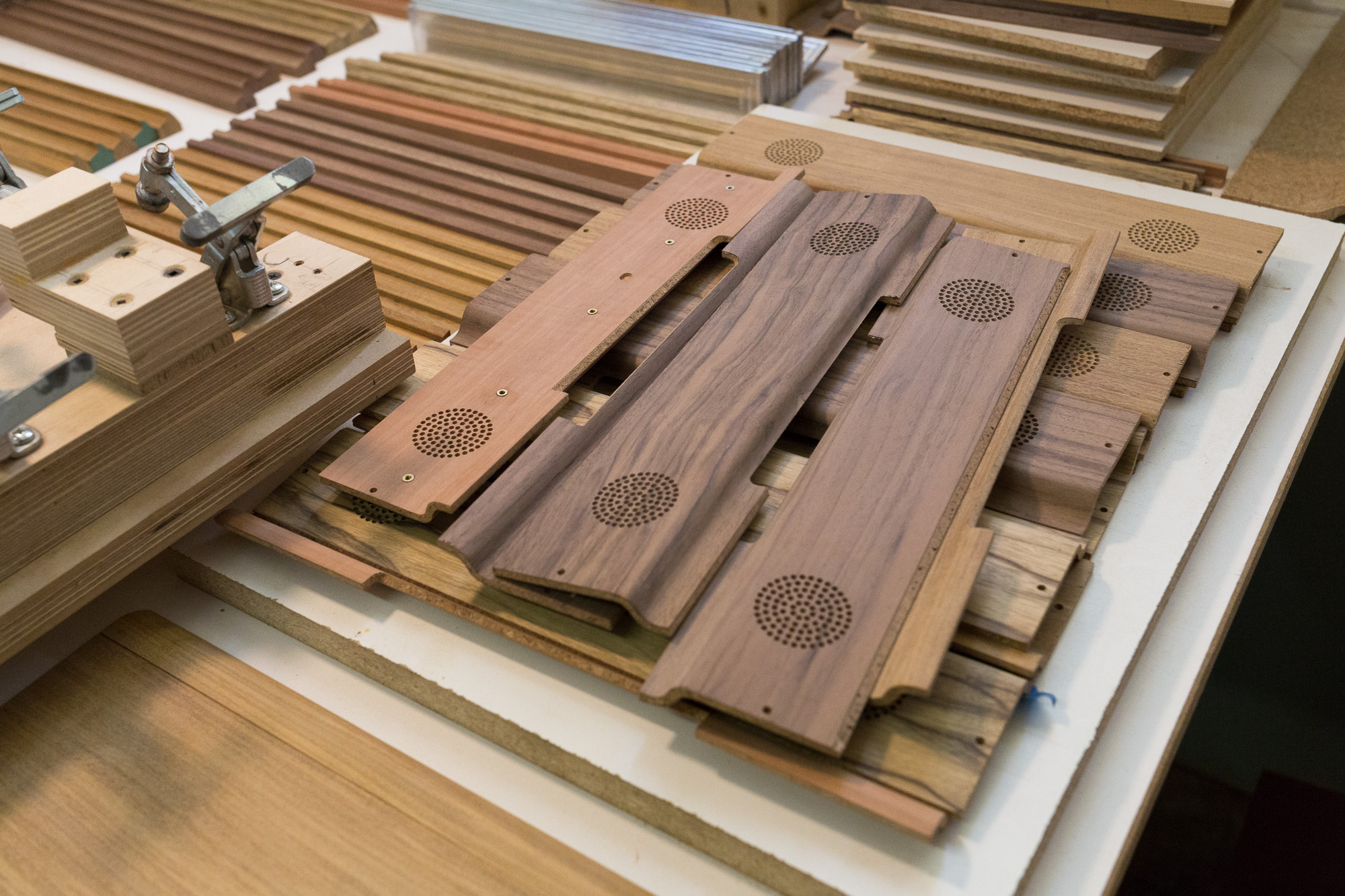
There’s a lot of science and engineering going into the Heirloom laptops. For starters, Kurt has created a unique composite material by layering cork, fiberglass, and wood. To help characterize the novel composite, some material samples were taken to the Center for Bits and Atoms at MIT, where Nadya Peek (who helped define the Peek Array) and Will Langford characterized the performance of the material. We took sections of the wood composite and performed a 3-point bend test using a Instron 4411 electromechanical material testing machine. From the test data, we were able to extract the flexural modulus and flexural strength of the material.
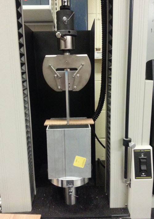
Heirloom composite material loaded into the testing machine
I’m not a mechanical engineer by training, so words like “modulus” and “specific strength” kind of go over my head. But Nadya was kind enough to lend me some insight into how to think about materials in this context. She pointed me at the Ashby chart, which like some xkcd comic panels, I could stare at for an hour and still not absorb all the information contained within.
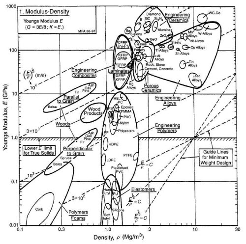
For example, the Ashby chart above plots Young’s Modulus versus density of many materials. In short, the bottom left of the chart has bendy, light materials – like cork – and the top right of the chart has rigid, heavy materials, like Tungsten. For a laptop case, we want a material with the density of cork, but the stiffness of plastic. If you look at the chart, wood products occupy a space to the left of plastics, meaning they are less dense, but they have a problem: they are weak perpendicular to the grain, and so depending on the direction of the strain, they can be as yielding as polyethene (the stuff used to make plastic beverage bottles), or stiffer than polycarbonate (the stuff layered with glass to make bulletproof windows). Composite materials are great because they allow us to blend the characteristics of multiple materials to hit the desired characteristic; in this case, Kurt has blended cork, glass fiber, and wood.
The measurements of the Heirloom composite show a flexural strength of about 33 MPa, and a flexural modulus of about 2.2-3.2 GPa. The density of the material is 0.49 g/cm3, meaning it’s about half the density of ABS. Plotting these numbers on the Ashby chart shows that the Heirloom composite occupies a nice spot to the left of plastics, and provides a compromise on stiffness based on grain direction.

The red circle shows approximately where the Heirloom composite lands. To be fair, measurements still revealed some directional sensitivity to the composite; depending on the grain, the modulus varies from about 2.2GPa to 3.2 GPa (and the diameter of the red circle encompasses this variability); but this is a much tighter band than the 10x difference in modulus indicated for pure woods.
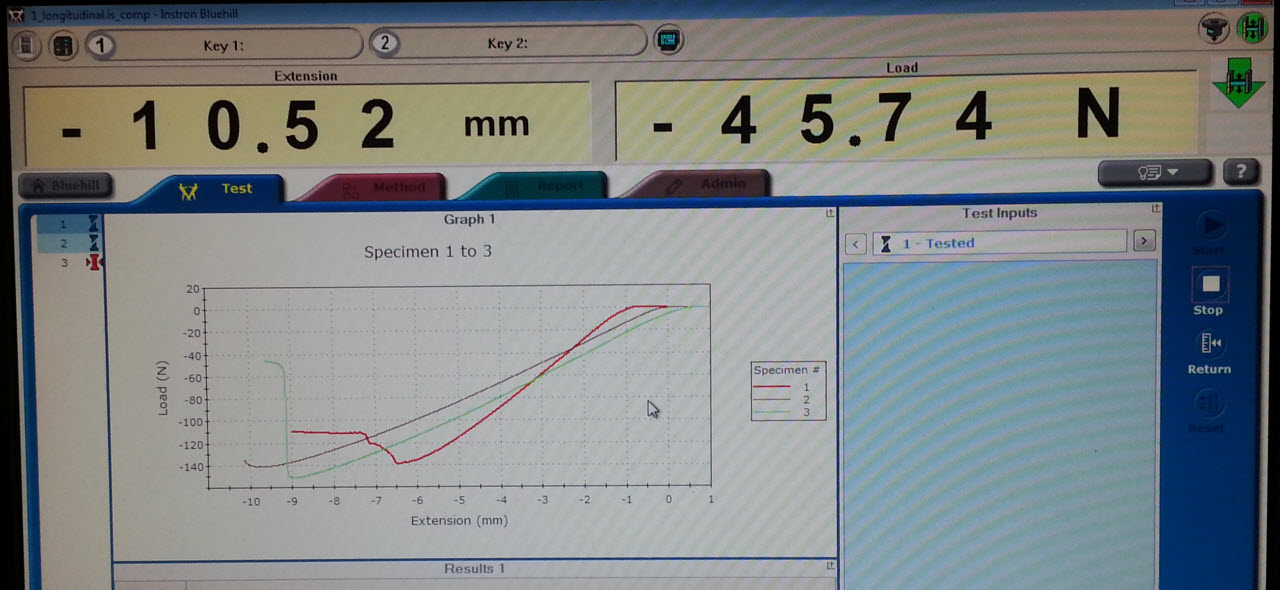
Another thing to note is that during testing, the material didn’t fail catastrophically. Above are the graphs of load vs. extension as plotted by the Instron testing machine. Even after bending the material past its peak load, it was still mostly intact and providing resistance. This result is a bit surprising; we had expected the material, like normal wood, would break in two once it failed. Furthermore, after we reset the test, the material bounced back to its original shape; even after bending by over 10mm, once the load was removed you could barely tell it went through testing. This high fracture toughness and resilience are desireable properties for a laptop case.
Of course, there’s nothing quite like picking up the material, feeling its surprising lightness, and then trying to give it a good bend and being surprised by its rigidity and ruggedness. The Heirloom backers will get the privilege of feeling this firsthand; for the rest of us, we’ll have to settle with seeing circles on Ashby charts and graphs on computer screens.
If you want to see more photos of the Heirloom laptop coming together, check out the image gallery at the bottom of the official Crowd Supply update!