Today, my collaborator Jie Qi and I launched a Crowd Supply campaign for circuit stickers.
Please visit the campaign page to see more photos of the stickers and to see how they can be used.
Here, I will write a bit about the background story, tech details, and manufacturing processes that went into making them.
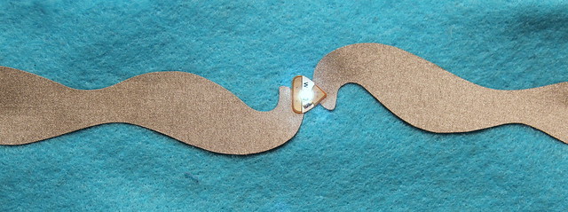
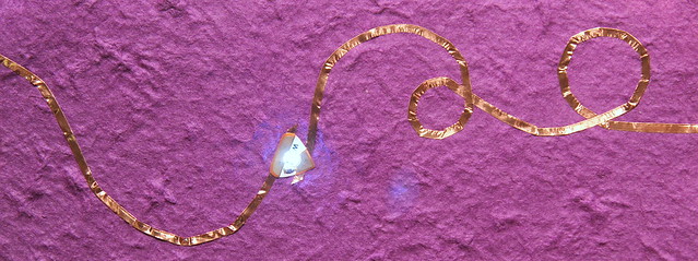
Circuit stickers are peel-and-stick electronics for crafting circuits. In a nutshell, they are circuits on a flexible polyimide substrate with anisotropic tape (or “Z-tape” — so named because electricity only flows vertically through the tape, and not laterally) laminated on the back.
The use of Z-tape allows one to assemble circuits without the need for high-temperature processing (e.g. soldering or reflow), thereby enabling compatibility with heat-sensitive and/or pliable material substrates, such as paper, fabric, plastic, and so forth.
This enables electronics to be integrated in a range of non-traditional material systems with great aesthetic effect, as exemplified by the addition of circuit stickers to fabric and paper, shown below.
The Backstory
In today’s world of contract manufacturing and turnkey service providers, designers tend to pick from a palette of existing processes to develop products. Most consumer electronic devices are an amalgamation of rigid PCB, reflow/wave soldering, ABS/PC injection molding, sheet metal forming, and some finishing processes such as painting or electroplating. This palette is sufficient to cover the full range of utility required by most products, but I’ve noticed that really outstanding products also tend to introduce new materials or novel manufacturing processes.
I’ve a long-running hypothesis that new process development doesn’t have to be expensive, as long as you yourself are willing to go onto the factory floor and direct the improvements. In other words, the expensive bit is the wages of the experts developing the process, not the equipment or the materials.
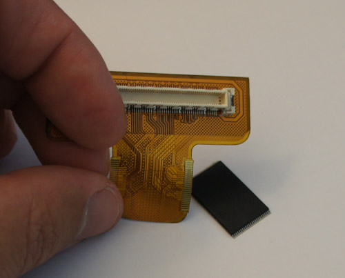
I decided to start exploring flex circuits as a design medium, under the reasoning that although flex circuit technology is common place inside consumer products — there’s probably a half dozen examples of flex PCB inside your mobile phone — it’s underrepresented in hobby & DIY products. I had a hunch that the right kind of product designed in flex could enable new and creative applications, but I wasn’t quite sure how. One of my “training exercises” was a flex adapter for emulating a TSOP NAND FLASH chip, which I had written about previously on this blog.
The moment of serendipity came last January, when I was giving a group of MIT Media Lab students a tour of Shenzhen. Jie Qi, a PhD candidate at the Media Lab, showed me examples of her work combining electronics and papercraft.

Clearly, circuits on flex could be an interesting addition to this new media, but how? Building circuits on flex and then soldering the flex circuit onto paper would be an improvement, but it’s only an incremental improvement. We wanted a solution that would be compatible with low-melting point materials; furthermore, being solder-free meant that the stickers could be used in contexts where using a soldering iron is impractical or prohibited.
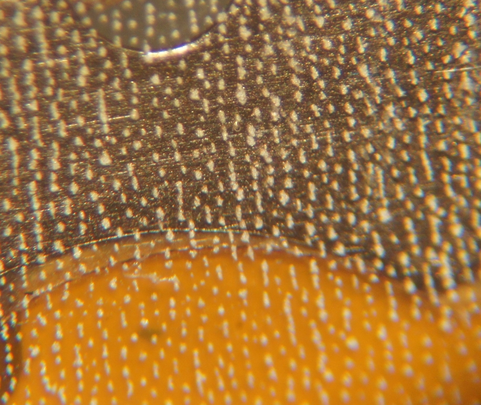
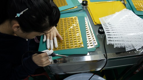
Jie introduced me to Z-tape, which is a great solution to the problem. November’s ware is a 20x magnification of Z-tape laminated to the back of a circuit sticker (someone has, of course, already correctly guessed the ware at the time of writing, so I can discuss the ware in more detail here without ruining the contest).
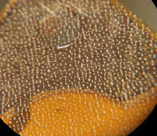
The stipples in the photo above (click on it for a larger version) are tiny metal particles that span from one side of the adhesive layer to the other. As you can see, the distribution is statistical in nature; therefore, in order to ensure good contact, a large pad area is needed. Furthermore, traces very close to each other can be shorted out by the embedded metal particles, so as I design the circuits I have to be careful to make sure I have enough space between exposed pads. The datasheet for the Z-tape material contains rules for the minimum pad size and spacing.
The problem is that there were no standard manufacturing processes that could produce circuit stickers as we envisioned them. Here at last was a meaningful opportunity to test the theory that new process development can be done on the cheap, as long as you are willing to do it yourself. And so, I started my own little research program to explore flexible circuit media, and the challenges of making circuit stickers out of them, all on Studio Kosagi’s shoe string R&D budget.
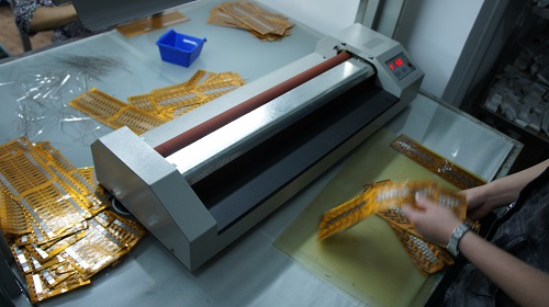
The first thing I did was to visit the facility where flex PCBs are manufactured. The visit was eye-opening.
Above is a worker manually aligning coverlay onto flex circuit material. Coverlay is a polyimide sheet used instead of soldermask on flex circuits. Soldermask is too brittle, and will crack; therefore, for reliability over thousands of flexing cycles, a coverlay is recommended.
Above is an example of steel plates being laminated to the back of flex circuit material. In some situations, it’s desirable for portions of the flex circuit to be stiff: either for mechanical mounting, or to help with SMT processing. I knew that it was possible to laminate polyimide stiffiners to flex, but I didn’t know that steel lamination was also possible until I took the factory tour.

Above is an example of the intricate shapes achievable with die cutting.
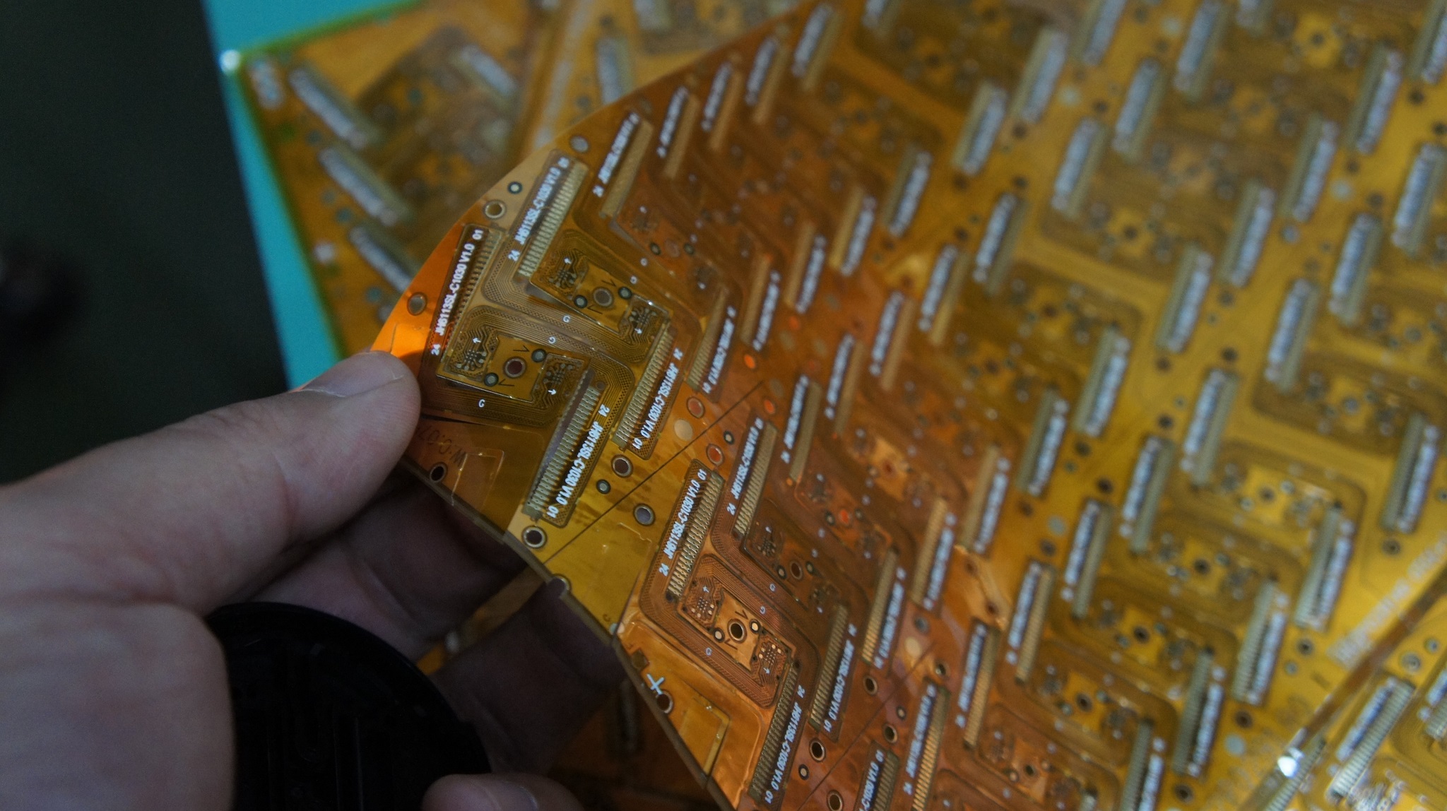
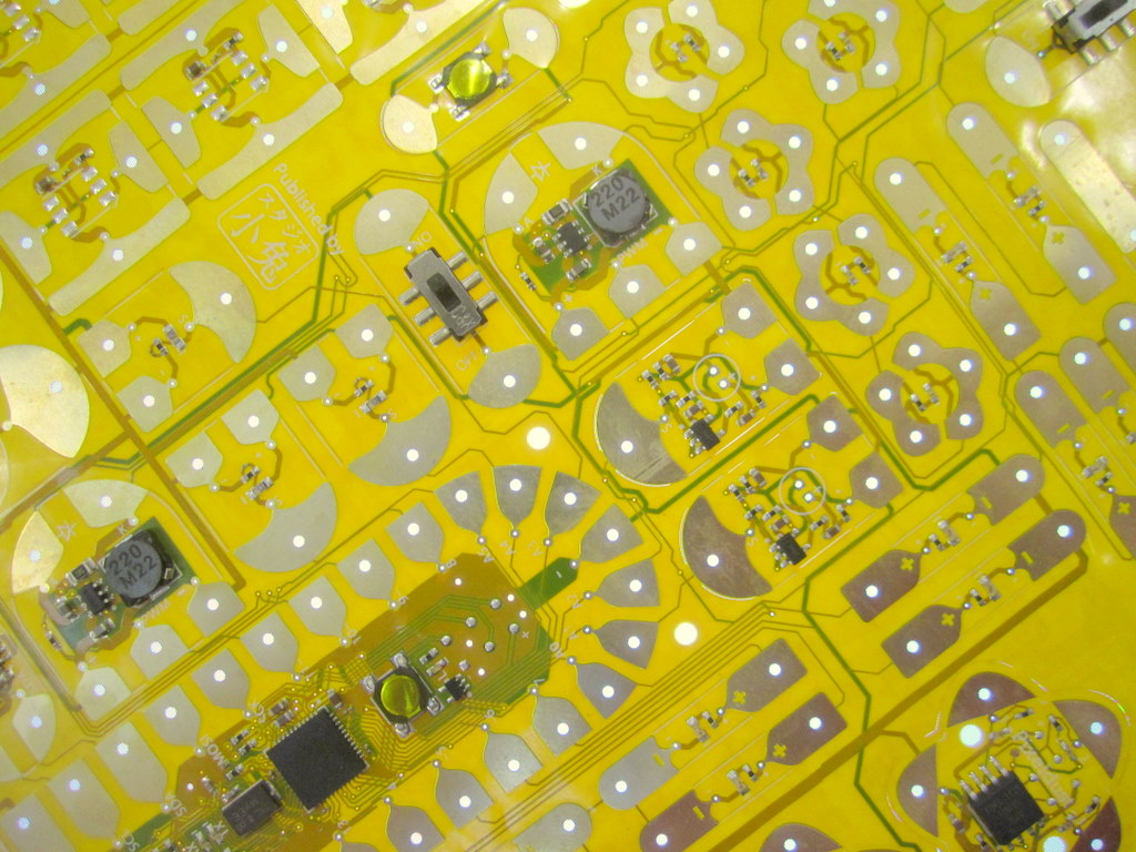
After visiting the factory, we decided the next step was to do a process capability test. The purpose of this test is to push the limits of the manufacturing process — intentionally breaking things to discover the weak links. Our design exercised all kinds of capabilities — long via chains, 3-mil line widths, 0201 components, 0.5mm pitch QFN, bulky components, the use of soldermask instead of coverlay, fine detail in silkscreening, captive tabs, curved cut-outs, hybrid SMT and through hole, Z-tape lamination, etc.
Below are some images of what our process capability test design looked like.

When I first presented the design to the factory, it was outright rejected as impossible to manufacture. However, after explaining my goals, they consented to produce it, with the understanding that I would accept and pay for all the units made including the defective units (naturally). Through analyzing the failure modes of the defective units, I was able to develop a set of design rules for maintaining high yield (and therefore lowering cost) on the circuit stickers.
In my next post on chibitronics, I’ll go into how we co-developed the final design and manufacturing process for the stickers. I will also have a post talking about how we developed the partial perforation die cut manufacturing process that enables the convenient peel-and-stick format for the stickers.
I’ll also have a post on why we decided to go with Crowd Supply instead of Kickstarter, and why we picked $1 as a funding goal.