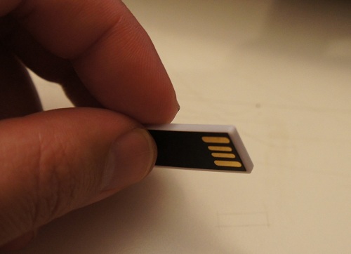
In January, I had the fortune of being a keynote speaker at LCA2013. One of the tchotchkes I received from the conference organizers was a little USB memory stick.

I thought it was a neat coincidence that I was in a factory that manufactured exactly such memory sticks about a week before the conference. In fact, I managed to score a rare treat: the factory owner gave me a sheet of raw chip-on-flex, prior to bonding and encapsulation, to take home.
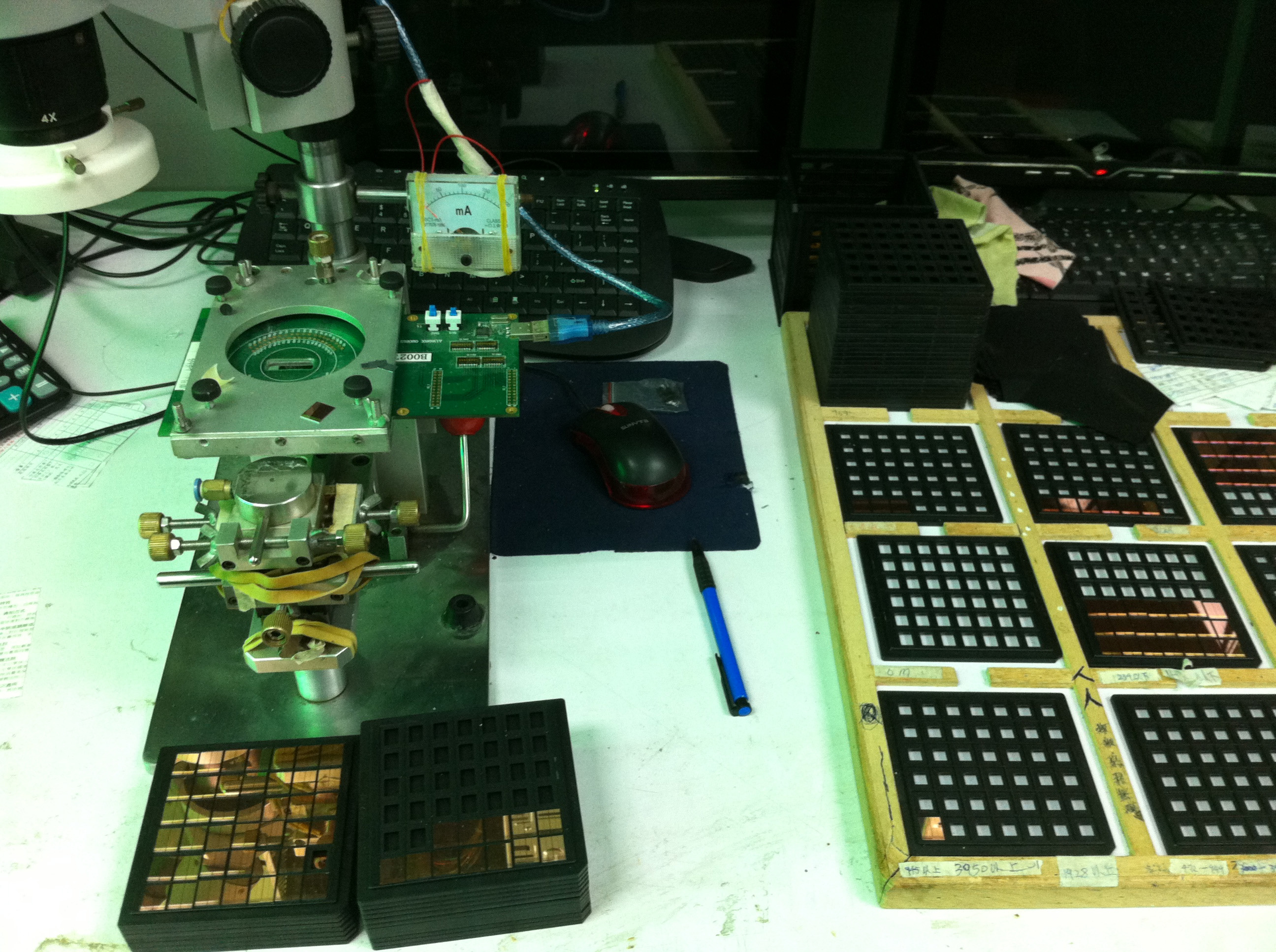
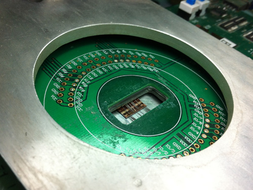
The USB sticks start life as bare FLASH memory chips. Prior to mounting on PCBs, the chips are screened for capacity and functionality. Below is a photo of the workstation where this happens:

In the image, you can see stacks of bare-die FLASH chips, awaiting screening with a probe card. I love the analog current meter and the use of rubber bands to hold it all together. The probe card has tiny needles on it that touch down on microscopic (less than 100-micron square) contacts on the chip surfaces. Below is what a probe card looks like.
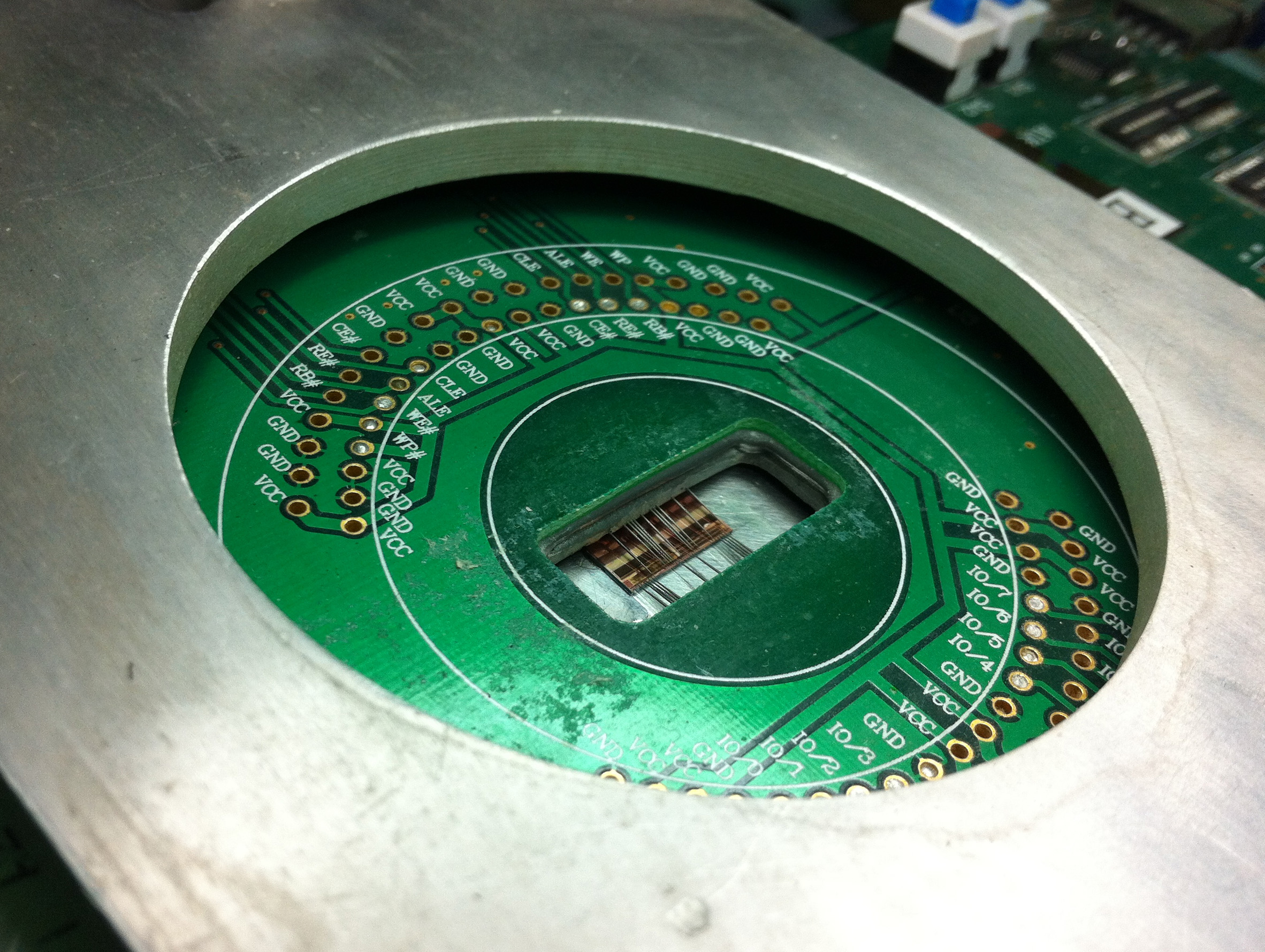
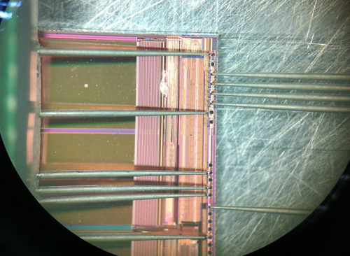
Below is an image through the microscope on the micro-probing station, showing the needles touching down on the square pads at the edge of the FLASH chip’s surface.
Interestingly, this all happens in an absolutely non-clean-room environment. Workers are pretty much handling chips with tweezers and hand suction vises, and mounting the devices into these jigs by hand.
Once the chips are screened for functionality, they are placed by hand onto a PCB. This is not an unusual practice, pretty much every value-oriented wirebonding facility I’ve visited relies on the manual placement of bare die. The photo below shows a controller IC being placed on a panel of PCBs. The bare die are in the right hand side of the photo, sitting in the beige colored waffle pack.

The lady is using some sort of tool made out of hand-cut bamboo. I still haven’t figured out exactly how they work, but every time I’ve seen this process they are using what looks like a modified chopstick to place the chips on the board. My best guess is that the bamboo sticks have just the right surface energy to adhere to the silicon die, such that silicon will stick to the tip of the bamboo rod. A dot of glue is pre-applied to the bare boards, so when the operator touches the die down onto the glue, the surface tension of the glue pulls the die off of the bamboo stick.
It’s trippy to think that the chips inside my USB stick were handled using modified chopsticks.

The chips are then wirebonded to the board using an automated bonding machine which uses image recognition to find the location of the bond pads (this is part of the reason they can get away with manual die placement).
(view in HD)
The first half of the video above starts out with the operator pulling off and replacing a mis-bonded wire by hand, and re-feeding the wire into the machine. Given that these wires are thinner than a strand of hair, and that the bonding pads are microscopic, this is no mean feat of manual dexterity.
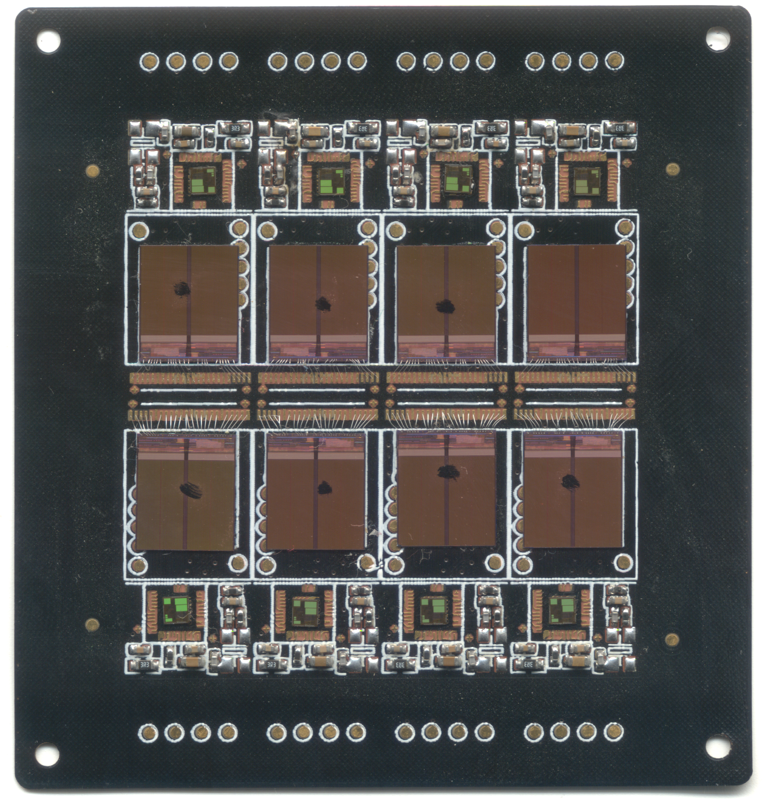
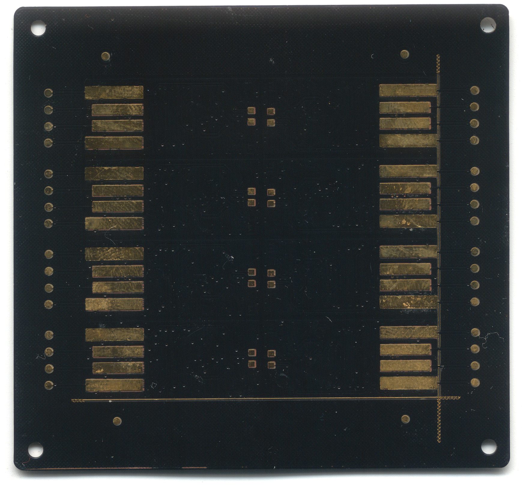
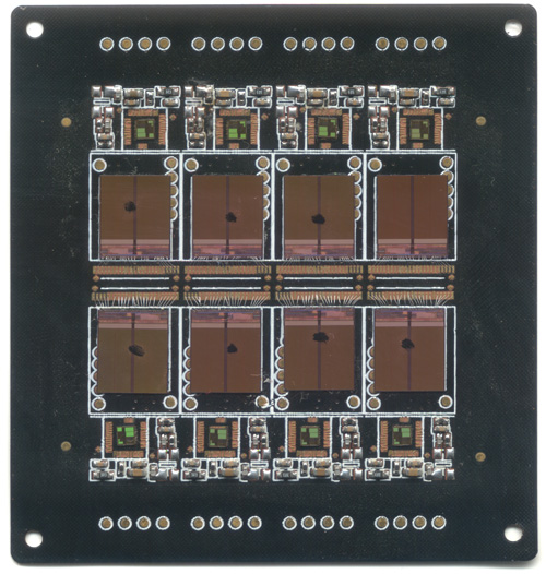
Here’s a scan of the partially-bonded but fully die-mounted PCB that I was given as a memoir from my visit (I had since crushed some of the wire bonds). The panel contains eight USB sticks, each consisting of a FLASH memory chip and a controller IC that handles the bridging between USB and raw FLASH, a non-trivial task that includes managing bad block maps and error-correction, among other things. The controller is probably an 8051-class CPU running at a few dozen MHz.

Once the panels are bonded and tested, they are overmolded with epoxy, and then cut into individual pieces, ready for sale.
Interestingly, the entire assembly prior to encapsulation is flexible. The silicon chips have been thinned down by grinding off their back sides to the point where they can tolerate a small amount of flexing, and the PCB is also so thin, it is flexible.

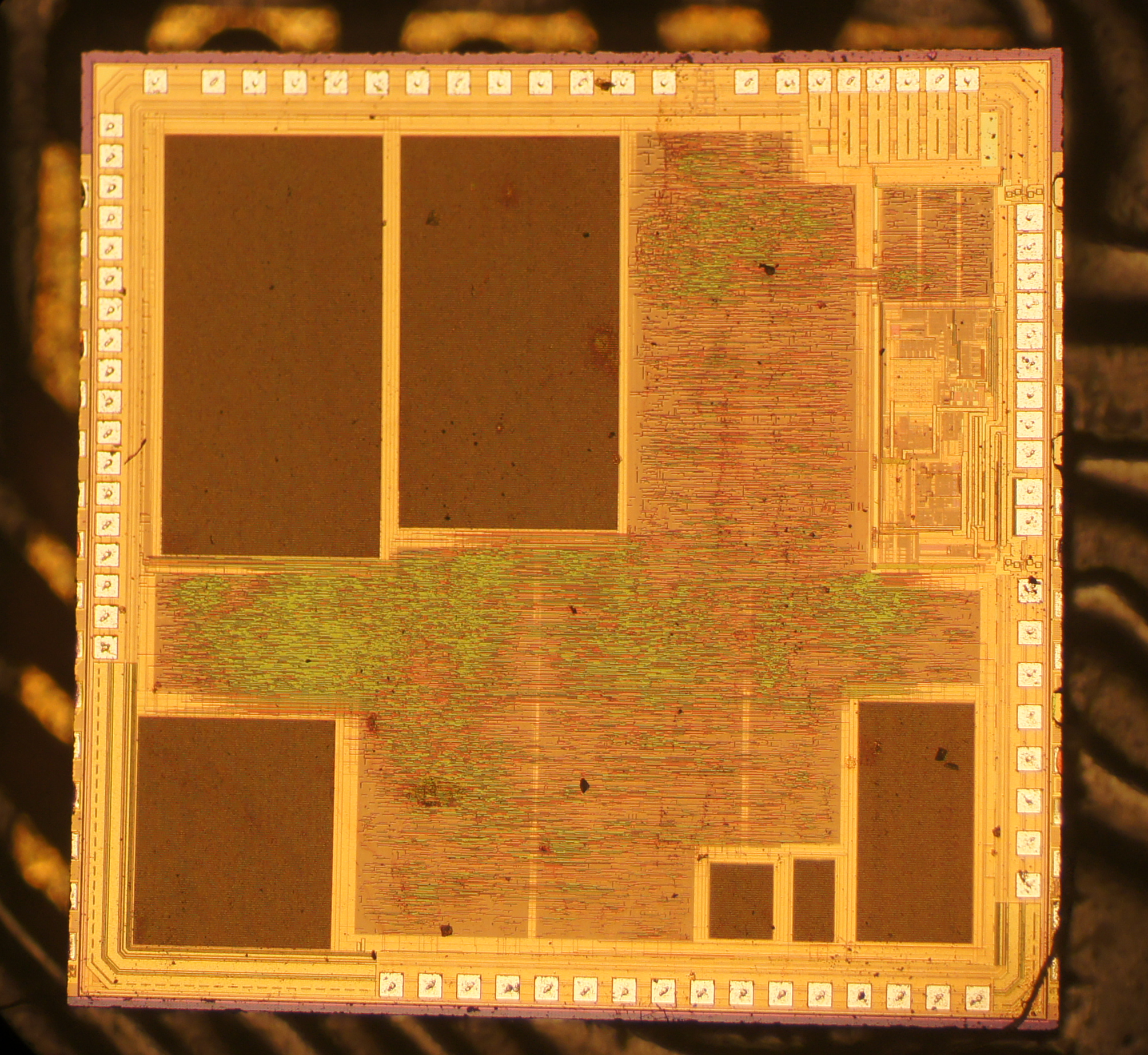
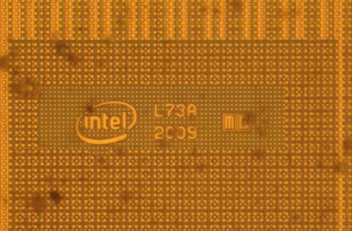
For those of you interested in this kind of thing, here’s the die marking from the FLASH chip; apparently it is made by Intel:
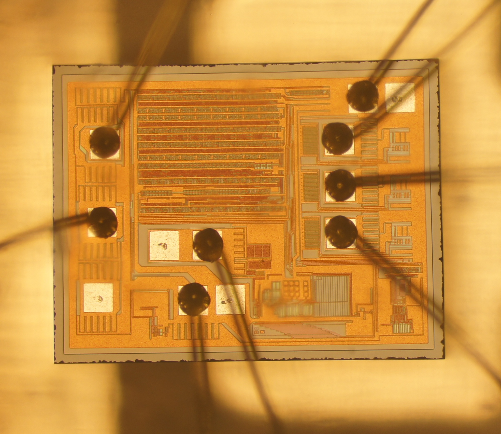
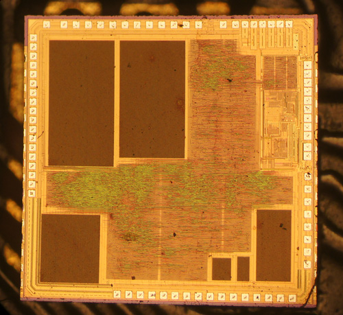
Here is also a die shot of the controller chip:
And now you know where those tiny USB thumb drives are born.
Thanks to David Cranor for contributing images. Images used with permission.
PS: chopsticks