Archive for the ‘chibitronics’ Category

Paper As a Substrate for Circuits

Tuesday, April 24th, 2018

I’ve spent a considerable portion of my time in the past couple of years helping to develop products for Chibitronics, a startup that blends two unlikely bedfellows together, papercraft and electronics, to create paper circuits. The primary emphasis of Chibitronics is creating a more friendly way to learn, design and create electronics. Because of this, much of the material relating to paper circuitry on the Internet looks more like art than electronics.

This belies the capabilities of paper as an engineering material. Google’s Cardboard and Nintendo’s Labo are mainstream examples of paper’s extraordinary capability as an engineering material. Prof. Nadya Peek at the University of Washington has written several academic papers on building multi-axis CNC machines using paper products.

A couple points to clarify up top: for the sake of brevity, I will use the term “paper” instead of “paper and/or cardboard”, analogous to how one would refer to a PCB made of Kapton or FR-4 both as printed circuits. Furthermore, while Chibitronics focuses on providing solderless solutions for younger learners, the techniques shared in this post targets engineers who have the skill to routinely assemble modern SMT designs. I assume you’ve got a good soldering iron and a microscope, and you know how to use both (or perhaps are up to the challenge of learning how to use them better).

The Argument for Paper
For prototyping and learning the principles of electronics, paper has several distinct advantages over breadboards.

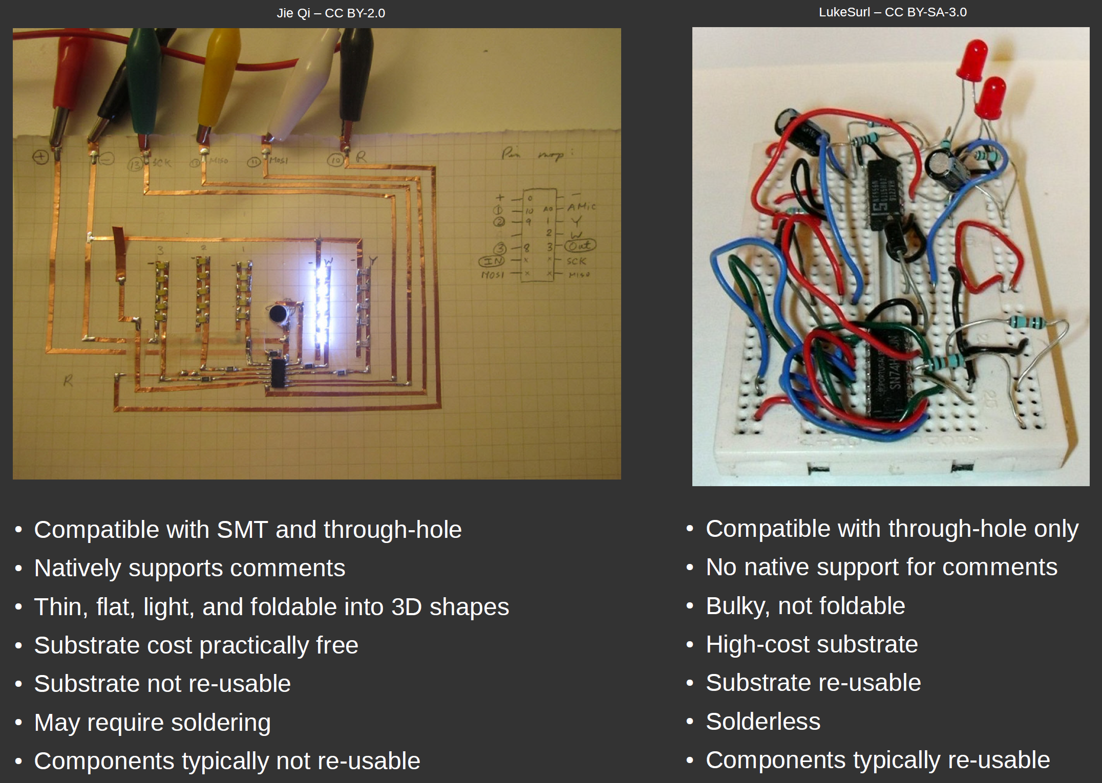
The primary advantage of a breadboard is that it’s solderless, and as a result you can re-use the components. This made a lot more sense back when a 6502 used to cost $25 in 1975 ($115 in 2018 money), but today the wire jumper kit for a solderless breadboard can cost more than the microcontroller. Considering also the relatively high cost of a solderless breadboard and the relatively low value of the parts, you’re probably better off buying extra parts and soldering them to disposable paper substrates than purchasing a re-usable solderless breadboard for all but the simplest of circuits.


Electronic components used to be really expensive, so you wanted to re-use them as much as possible. The 8-bit 6502 at $115 (adjusted for inflation) was considerably cheaper than its competition in 1975 (from Wikipedia).

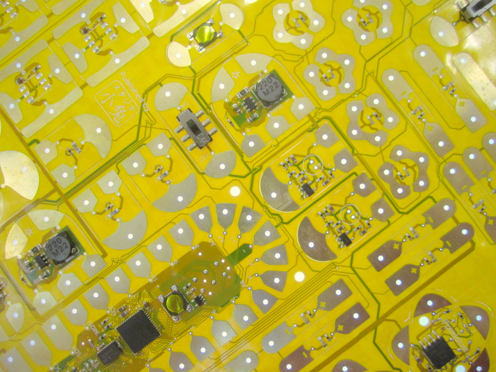
On the other hand, paper has a number of important advantages. The first is that it’s compatible with surface mount ICs. This is increasingly important as chip vendors have largely abandoned DIP packages in favor of SMT packages: mobile computing represents the highest demand for chips, and SMT packages beat DIP packages in both thermal and parasitic electrical characteristics. So if you want a part that wasn’t designed by someone wearing a jean jacket and highwaters, you’re probably going to find it only available in SMT.


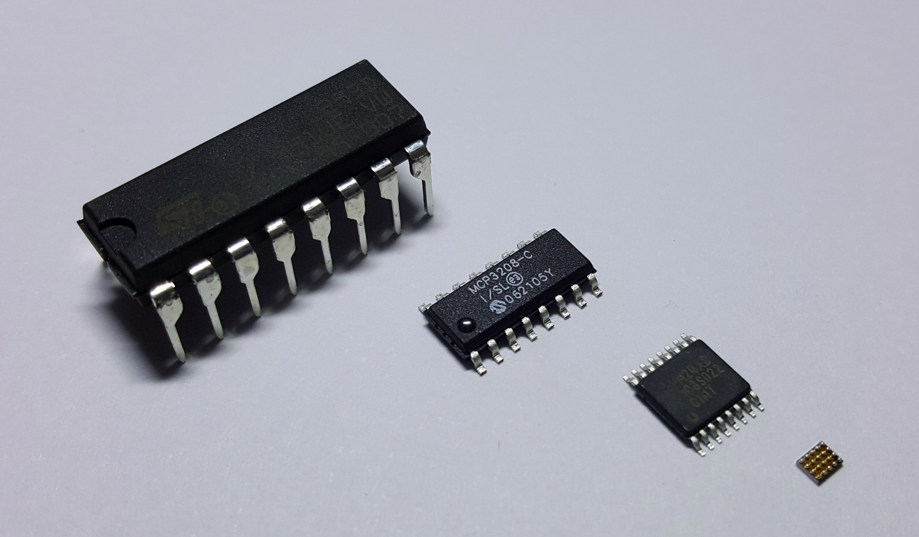
The evolution of packaging (from left to right): DIP, SOIC, TSSOP, and WLCSP. The WLCSP is shown upside-down so you can see how solder balls are applied directly to a naked silicon chip. It’s the asymptotic size limit of packaging, and is quite popular in mobile phones today.

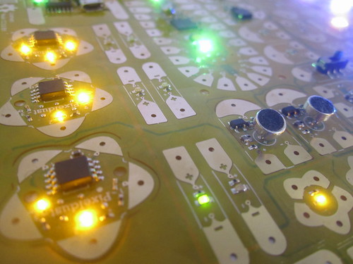
The second and perhaps more important advantage is that it’s electrically similar to a printed circuit substrate. Breadboards feature long, loose wires with no sense of impedance control at all. Printed circuits are 2.5-D (e.g. planar multi-layer) constructions that feature short, flat wires and often times ground planes that enable impedance control. Paper circuit construction is much closer to that of a printed circuit, in that flat copper tape forms traces that can be layered on top of each other (using non-conductive tape to isolate the layers). Furthermore, when laid on top of a controlled-thickness substrate such as cardboard, the reverse side can be covered with a plane of copper tape, thus allowing for impedance control. The exact same equations govern impedance control in a paper circuit constructed with a ground plane as a printed circuit constructed with a ground plane – just the constants are different.


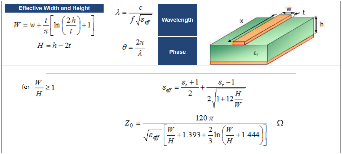
This equation works for both FR-4 and cardboard. Just plug in the corresponding ε, w, t, and h. From rfcafe.com.

This means you can construct RF circuits using paper electronic techniques — from directional couplers to antennae to amplifiers. The low parasitics of copper tape also means you can construct demanding circuits that would be virtually impossible to breadboard, such as high-power switching regulators, where ripple performance is heavily impacted by parasitic resistance and inductance in the ground connections.


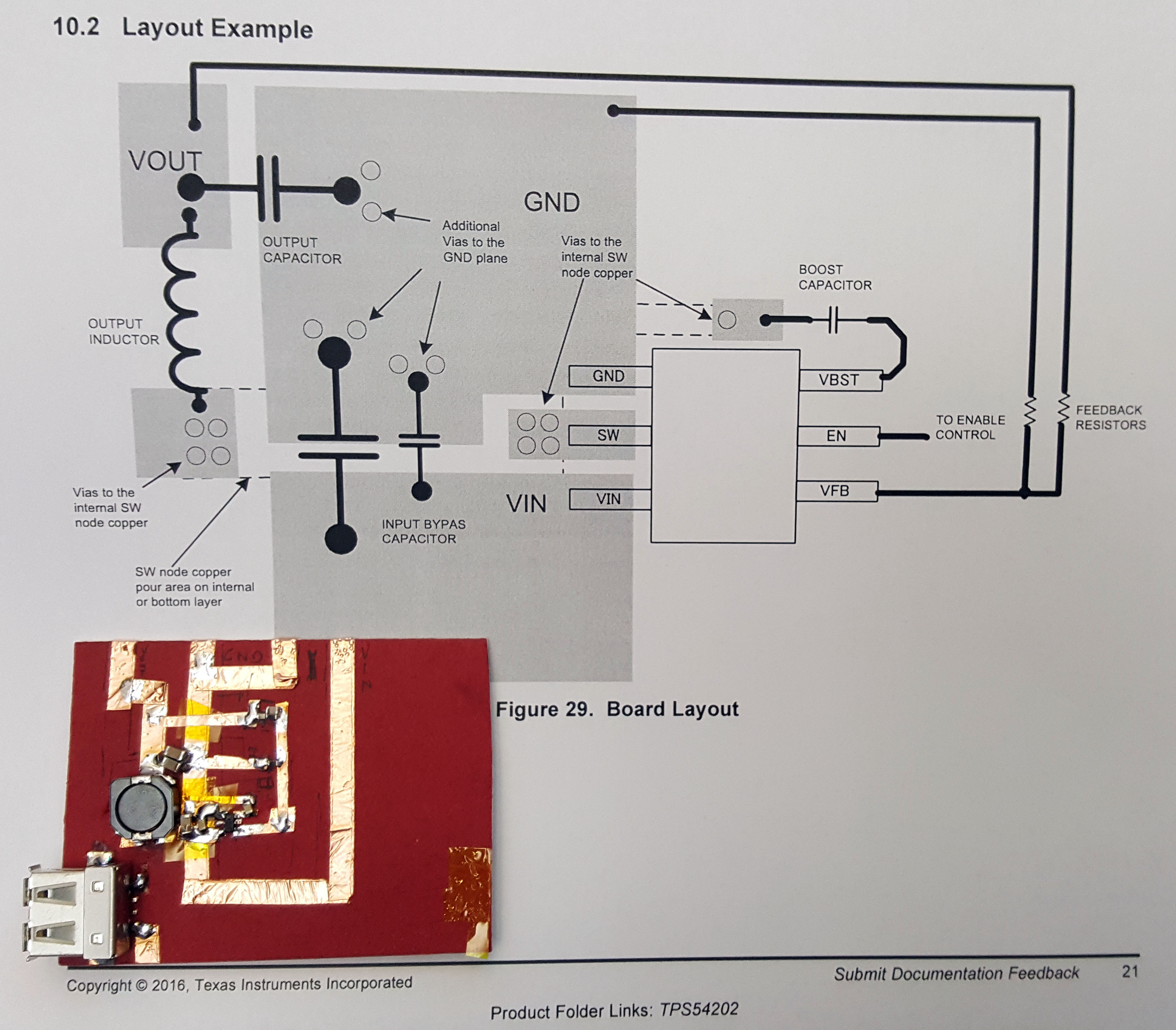
A 10W, 5V buck regulator laid out with paper electronics. The final layout closely resembles the datasheet layout example and performs smoothly at 2A load; this circuit probably wouldn’t regulate properly at high loads if built with a SMT-to-DIP breakout and a breadboard.

In addition to impedance control and lower parasitics, the use of copper tape to form planes means paper electronics can push the power envelope by leveraging copper plans as heatsinks. This is an important technique in FR-4 based PCBs; in fact, for many chips, the dominant path for heat to escape a chip is not through the package surface, but instead through the pins and package traces.


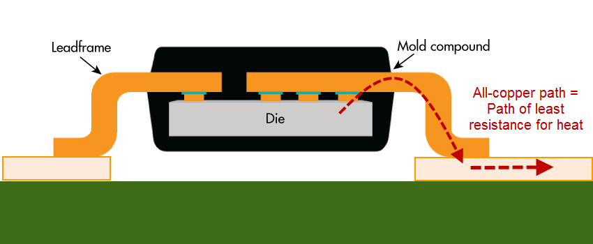
Copper conducts heat about 1000x better than plastic, so even the tiny metal pins on a chip can conduct heat more efficiently from an IC than the surface of the plastic package. Flip-chip on lead frame graphic adapted from Electronic Design.

The copper which forms the pins and lead frames of a chip package is a vastly superior (about 1000x better) heat conductor compared to air or plastic, so a cheap and effective method of heatsinking is to lay out a large plane of copper connected to the chip. Below is an example of a 60-watt power driver that I built using paper electronics, leveraging a copper tape plane plus extra foil as heat sinks.


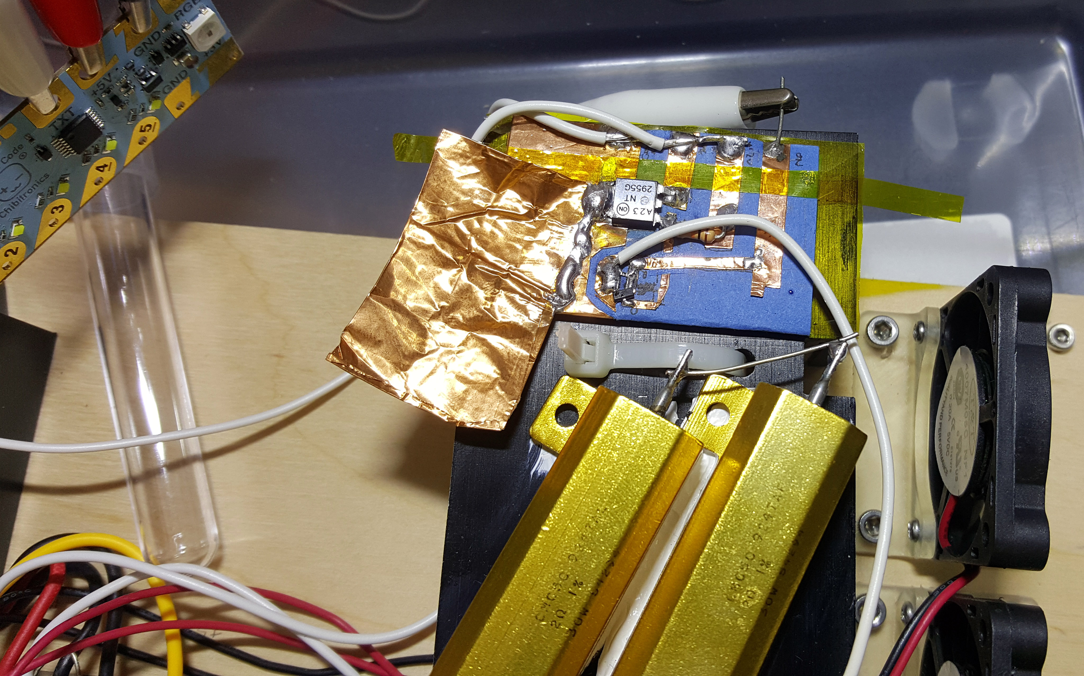
That’s a 12A power transistor, and this heater control circuit can use much of that ampacity. Additional copper foil was soldered on for extra heat sinking. The equivalent in DIP/TO packages might melt a breadboard during normal operation.

Paper electronics has one additional advantage that is unique to itself: the ability to fold and bend into 3-dimensional shapes. This is something that neither breadboards nor FR-4 circuit boards can readily do. Normally, circuit boards that can bend require more exotic processes like rigi-flex or flex PCB manufacture; but paper supports this natively. Artists take advantage of this property to create stunning electronic origami, but engineers can also use this property to great effect.


Trox Circuit Study 05 by Jonathan Bobrow, from the Paper Curiosities gallery

The ability to fold a sheet of cardboard or paper means that paper circuits can be slotted around tight corners and conformed to irregular or flexible surfaces, eliminating connectors and creating a thinner, sleeker packages. Need a test point? Cut a hanging tab out of your substrate, and you’ve got a fold-up point where you can attach an alligator clip!

Using Paper to Facilitate Prototyping with SMT
Here’s a detailed example of the construction techniques I use when working with paper electronics. I built a breakout board to solve a common problem: matching voltages between chips. Older chips are powered by 5V, newer ones by 1.8V or lower, and none of these are a match for your typical 3.3V-tolerante microcontroller. There are small circuits called “level shifters” that can safely take digital signals of one signal swing to another range. The problem is that most of the “good” ICs today come only in SMT packages, so if you’re prototyping on a breadboard or using alligator clips to cobble something together, you’ve got very limited options. In fact, one of my “go-to” ICs for this purpose is the 74LVC1T45; it’s capable of 420Mbps data rates, and can convert anywhere from 1.65V to 5.5V in a direction that can be selected using an input pin. The packaging options for this chip range from a DSBGA to a SOT-23 – clearly a chip targeted at the mobile phone generation, and not meant for breadboarding.

However, I’m often confronted with the problem of driving a WS281B LED strip from the I/O of a modern microprocessor. WS2812B LEDs operate off of 5V, and expect 5V CMOS levels; and no modern microprocessor can produce that. You can usually get away with driving a single WS2812B with a 3.3V-compatible I/O, but if you’re driving a long chain of them you’ll start to see glitches down the chain because of degraded timing margins due to improper voltage levels at the head of the chain. So, I’d love to have a little breakout board that adapts a SOT-23-sized 74LVC1T45 to an alligator-clip friendly format.

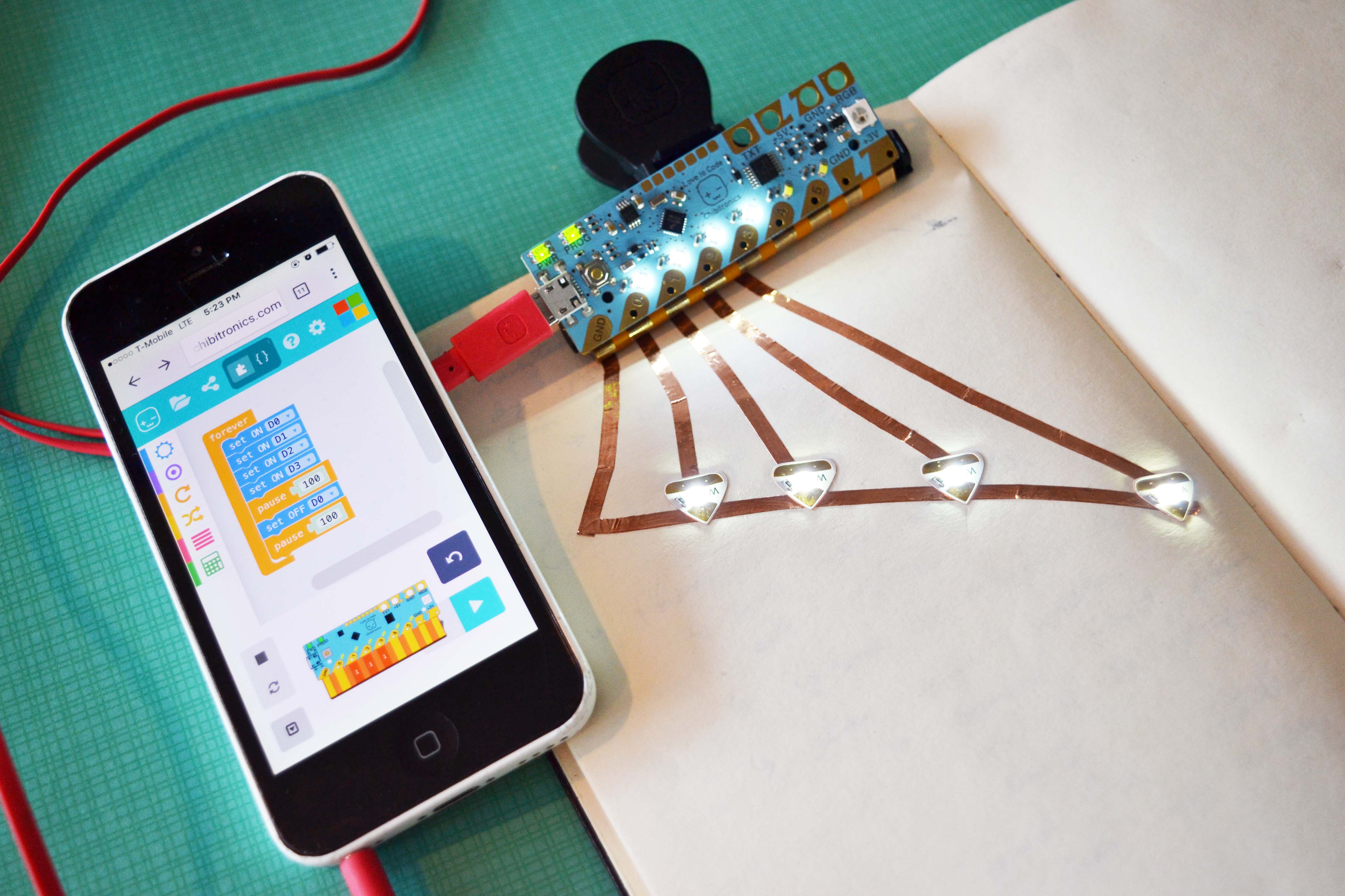
Instead of laying out a PCB, fabbing a one-off, and soldering it together, I took a piece of cardboard and built a breakout board in under an hour. Furthermore, because I can bend cardboard, I can make my breakout board dual-purpose: I can add pins to it that make it breadboard-compatible, while having fold-up “wings” for alligator clips. Without the ability to fold up, the alligator clip extensions would block access to the breadboard connections. Below are some shots of the finished project.


Native comments plus on-board decoupling caps makes this simple to use, even with long alligator clips


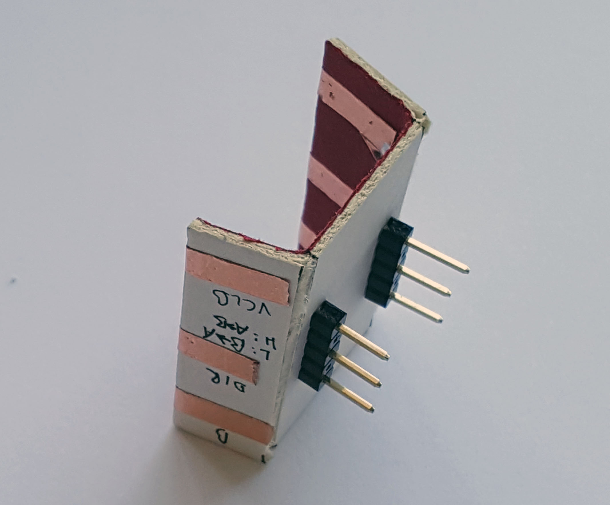
DIP pins coming out the bottom side allow this to be used in a breadboard, too


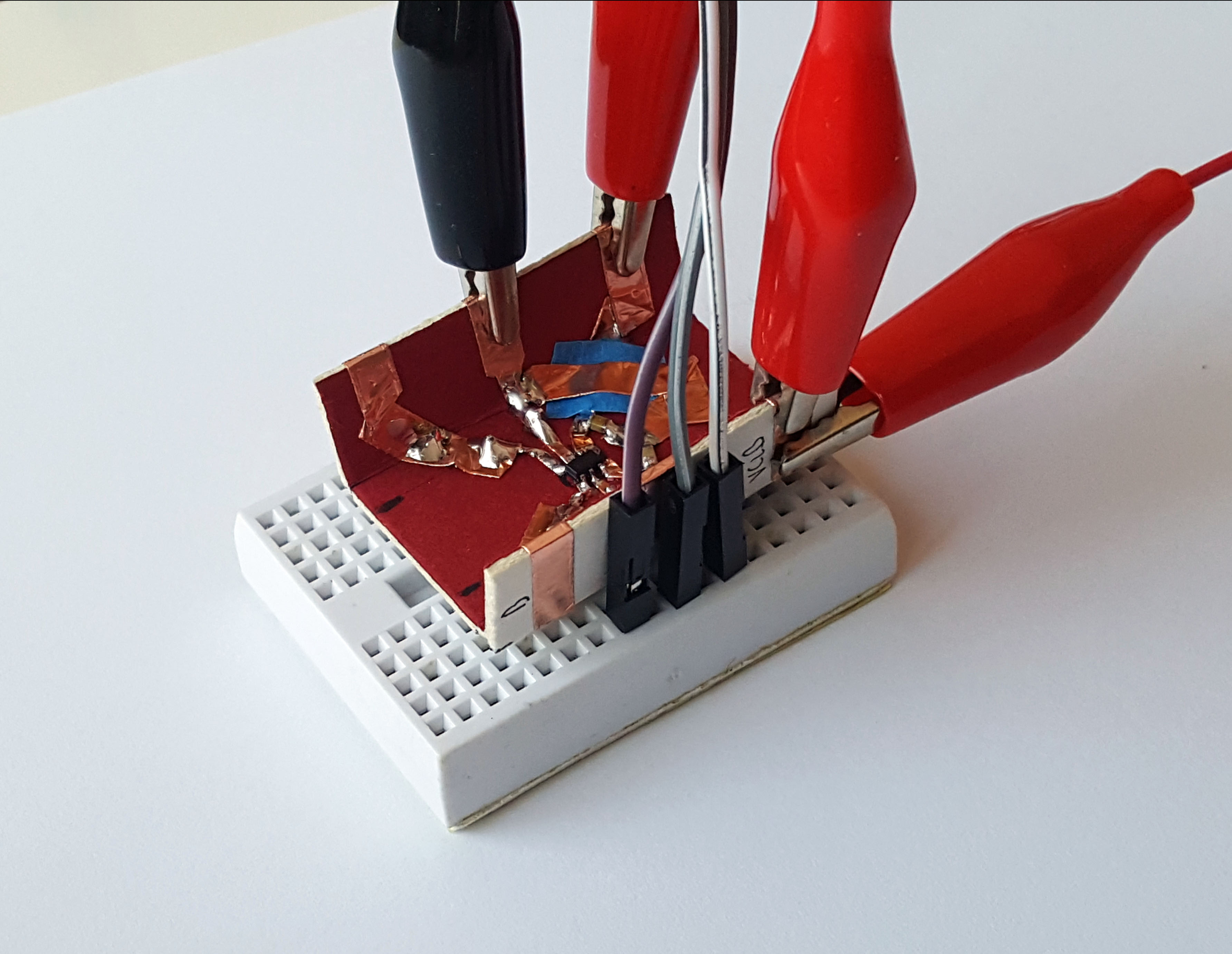
SMT, DIP, and alligator clips all coexisting in a single breakout — easy to do with paper!

The first step in making a paper circuit is to grab a suitable piece of cardboard. I’ve come to really enjoy the cardboard used to make high-quality mats for picture framing. It’s about 1.3-1.4mm thick, which is fairly similar to FR-4 thickness, and its laminate structure means you can score one side and make accurate folds into the third dimension. The material is also robust to soldering temperatures, and its dense fiber construction and surface coating keeps the paper surface intact when pulling off mild adhesives, like the ones found on copper tape.

I’ll then cut out a square about the size I think it needs to be. I’ll usually cut a little larger, because it’s trivial to trim it back later on, but janky to tape on an extension if it’s too small.

Then, I lay the components on top and sketch a layout – this one’s pretty simple, I just note where I want the SOT-23 to go, and where the breakouts should run to.

Once I’m happy with the sketch, I’ll lay down copper tape, solder on the components, and then fold/bend the breakout into the final shape.

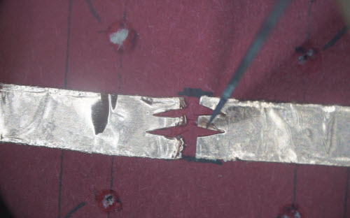
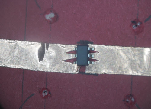
The trickiest and most important technique to master is how to mate the copper tape to the tiny pins of the SOT-23 (or other SMT) package. I use a trick that Dr. Jie Qi taught me, which is to cut a set of triangular notches into the tip of a wider piece of copper tape of roughly the right pitch. The triangular shape lets you adjust the size of the landing pad by simply changing the gap between the two ends of the tape, alleviating the need for precise alignment. Then, once the component is soldered to the wide piece of copper tape, you take a knife and cut the tape into individual traces – voilà, an SMT breakout is born!

A lot of this is better shown not told, so I’ve created a little video, below, that walks you through the entire process of building the breakout.

Try Something Different, and You Might be Rewarded!
Paper as an electrical engineering material is something I would never have thought of on my own – I grew up prototyping with breadboards and wire-wrap, and I was prejudiced against paper as a cheap, throwaway material that I incorrectly thought was too flammable to solder. Instead, I spent hundreds of dollars on breadboards and wire wrap sockets, when I could have made do with much cheaper materials. Indeed, there is an irrational psychology that regards expensive things as inherently better than cheap things, which means cheap options are often overlooked in the search for solutions to hard problems.

But this is why it’s important to collaborate with experts outside your normal field of expertise – the further outside, the better. In addition to being a great engineer, Jie Qi is a prodigious artist. Through our Chibitronics collaboration, she’s added so much more depth and dimension to my world on so many fronts. She’s imparted upon me invaluable gifts of skills and perspectives that I would never have developed otherwise.

It’s my hope that by sharing a little more about paper electronics, I can bring a fresh perspective on old problems while broadening awareness and getting more users to improve upon the basics. After all, this is a new area, and we’re just starting to explore the possibilities.

Interested in hacking paper electronics? Check out the Chibitronics Creative Coding Kit, and the Love to Code product line. It’s a gentle introduction to paper electronics targeted at newcomers, but it’s also open source, so you can take it as far as your imagination can go — hook up a JTAG box, build the OS, and get hacking! Get 30% off the Creative Coding Kit with the TRY-LTC-18 coupon code until June 30, 2018!


Quick edit: some basic techniques on using copper tape are documented at Chibitronics’ Copper Tape Chronicles. It’s a small compilation of videos like the one below:

Also, here’s a handy tip on how to keep copper tape from falling off the roll:

Why I’m Using Bitmarks on my Products

Friday, October 13th, 2017

One dirty secret of hardware is that a profitable business isn’t just about design innovation, or even product cost reduction: it’s also about how efficiently one can move stuff from point A to B. This explains the insane density of hardware suppliers around Shenzhen; it explains the success of Ikea’s flat-packed furniture model; and it explains the rise of Amazon’s highly centralized, highly automated warehouses.

Unfortunately, reverse logistics – the system for handling returns & exchanges of hardware products – is not something on the forefront of a hardware startup’s agenda. In order to deal with defective products, one has to ship a product first – an all-consuming goal. However, leaving reverse logistics as a “we’ll fix it after we ship” detail could saddle the venture with significant unanticipated customer support costs, potentially putting the entire business model at risk.

This is because logistics are much more efficient in the “forward” direction: the cost of a centralized warehouse to deliver packages to an end consumer’s home address is orders of magnitude less than it is for a residential consumer to mail that same parcel back to the warehouse. This explains the miracle of Amazon Prime, when overnighting a pair of hand-knit mittens to your mother somehow costs you $20. Now repeat the hand-knit mittens thought experiment and replace it with a big-screen TV that has to find its way back to a factory in Shenzhen. Because the return shipment can no longer take advantage of bulk shipping discounts, the postage to China is likely more than the cost of the product itself!

Because of the asymmetry in forward versus reverse logistics cost, it’s generally not cost effective to send defective material directly back to the original factory for refurbishing, recycling, or repair. In many cases the cost of the return label plus the customer support agent’s time will exceed the cost of the product. This friction in repatriating defective product creates opportunities for unscrupulous middlemen to commit warranty fraud.

The basic scam works like this: a customer calls in with a defective product and gets sent a replacement. The returned product is sent to a local processing center, where it may be declared unsalvageable and slated for disposal. However, instead of a proper disposal, the defective goods “escape” the processing center and are resold as new to a different customer. The duped customer then calls in to exchange the same defective product and gets sent a replacement. Rinse lather repeat, and someone gets rich quick selling scrap at full market value.

Similarly, high-quality counterfeits can sap profits from companies. Clones of products are typically produced using cut-rate or recycled parts but sold at full price. What happens when customers then find quality issues with the clone? That’s right – they call the authentic brand vendor and ask for an exchange. In this case, the brand makes zero money on the customer but incurs the full cost of supporting a defective product. This kind of warranty fraud is pandemic in smart phones and can cost producers many millions of dollars per year in losses.


High-quality clones, like the card on the left, can cost businesses millions of dollars in warranty fraud claims.

Serial numbers help mitigate these problems, but it’s easy to guess a simple serial number. More sophisticated schemes tie serial numbers to silicon IDs, but that necessitates a system which can reliably download the serialization data from the factory. This might seem a trivial task but for a lot of reasons – from failures in storage media to human error to poor Internet connectivity in factories – it’s much harder than it seems to make this happen. And for a startup, losing an entire lot of serialization data due to a botched upload could prove fatal.

As a result, most hardware startups ship products with little to no plan for product serialization, much less a plan for reverse logistics. When the first email arrives from an unhappy customer, panic ensues, and the situation is quickly resolved, but by the time the product arrives back at the factory, the freight charges alone might be in the hundreds of dollars. Repeat this exercise a few dozen times, and any hope for a profitable run is rapidly wiped out.

I’ve wrestled with this problem on and off through several startups of my own and finally landed on a solution that looks promising: it’s reasonably robust, fraud-resistant, and dead simple to implement. The key is the bitmark – a small piece of digital data that links physical products to the blockchain.

Most people are familiar with blockchains through Bitcoin. Bitcoin uses the blockchain as a public ledger to prevent double-spending of the same virtual coin. This same public ledger can be applied to physical hardware products through a bitmark. Products that have been bitmarked can have their provenance tracked back to the factory using the public ledger, thus hampering cloning and warranty fraud – the physical equivalent of double-spending a Bitcoin.

One of my most recent hardware startups, Chibitronics has teamed up with Bitmark to develop an end-to-end solution for Chibitronics’ newest microcontroller product, the Chibi Chip.

As an open hardware business, we welcome people to make their own versions of our product, but we can’t afford to give free Chibi Chips to customers that bought cut-rate clones and then report them as defective for a free upgrade to an authentic unit. We’re also an extremely lean startup, so we can’t afford the personnel to build a full serialization and reverse logistics system from scratch. This is where Bitmark comes in.

Bitmark has developed a turn-key solution for serialization and reverse logistics triage. They issue us bitmarks as lists of unique, six-word phrases. The six-word phrases are less frustrating for users to type in than strings of random characters. We then print the phrases onto labels that are stuck onto the back of each Chibi Chip.


Bitmark claim code on the back of a Chibi Chip

We release just enough of these pre-printed labels to the factory to run our authorized production quantities. This allows us to trace a bitmark back to a given production lot. It also prevents “ghost shifting” – that is, authorized factories producing extra bootleg units on a midnight shift that are sold into the market at deep discounts. Bitmark created a website for us where customers can then claim their bitmarks, thus registering their product and making it eligible for warranty service. In the event of an exchange or return, the product’s bitmark is updated to record this event. Then if a product fails to be returned to the factory, it can’t be re-claimed as defective because the blockchain ledger would evidence that bitmark as being mapped to a previously returned product. This allows us to defer the repatriation of the product to the factory. It also enables us to use unverified third parties to handle returned goods, giving us a large range of options to reduce reverse logistics costs.

Bitmark also plans to roll out a site where users can verify the provenance of their bitmarks, so buyers can check if a product’s bitmark is authentic and if it has been previously returned for problems before they buy it. This increases the buyer’s confidence, thus potentially boosting the resale value of used Chibi Chips.

For the cost and convenience of a humble printed label, Bitmark enhances control over our factories, enables production lot traceability, deters cloning, prevents warranty fraud, enhances confidence in the secondary market, and gives us ample options to streamline our reverse logistics.

Of course, the solution isn’t perfect. A printed label can be peeled off one product and stuck on another, so people could potentially just peel labels off good products and resell the labels to users with broken clones looking to upgrade by committing warranty fraud. This scenario could be mitigated by using tamper-resistant labels. And for every label that’s copied by a cloner, there’s one victim who will have trouble getting support on an authentic unit. Also, if users are generally lax about claiming their bitmark codes, it creates an opportunity for labels to be sparsely duplicated in an effort to ghost-shift/clone without being detected; but this can be mitigated with a website update that encouraging customers to immediately register their bitmarks before using the web-based services tied to the product. We also have to exercise care in handling lists of unclaimed phrases because, until a customer registers their bitmark claim phrase in the blockchain, the phrases have value to would-be fraudsters.

But overall, for the cost and convenience, the solution outperforms all the other alternatives I’ve explored to date. And perhaps most importantly for hardware startups like mine that are short on time and long on tasks, printing bitmarks is simple enough for us to implement that it’s hard to justify doing anything else.

Disclosure: I am a technical advisor and shareholder of Bitmark.

See you at Maker Faire Bay Area!

Saturday, May 17th, 2014

Looking forward to seeing everyone at Maker Faire Bay Area, happening May 17 & 18 at the San Mateo Event Center. xobs and I will be giving a short half-hour talk starting at 10:30AM in the Expo hall on Saturday about Novena, on the Electronics stage. Afterwards, xobs will be hanging out with his Novena at the Freescale booth, also in the Expo hall, about halfway down on the left hand side across from the Atmel/Arduino booth. If you’re curious to see it or just want to stop by and say hi, we welcome you!

Also, the whole chibitronics crew will be in the Expo hall as well, in the second row between Sony, PCH, and Qualcomm (‽‽‽). We’ll be teaching people how to craft circuits onto paper; attendees who can score a first-come, first-serve spot will receive free circuit stickers and also get a chance to be instructed by the wonderful and dynamic creative genius behind chibitronics, Jie Qi.

Circuit Stickers Manufacturing Retrospective: From Campaign to First Shipment

Tuesday, April 29th, 2014

Last December, Jie Qi and I launched a crowdfunding campaign to bring circuit stickers under the brand name of “chibitronics” to the world.

Our original timeline stated we would have orders shipped to Crowd Supply for fulfillment by May 2014. We’re really pleased that we were able to meet our goal, right on time, with the first shipment of over a thousand starter kits leaving the factory last week. 62 cartons of goods have cleared export in Hong Kong airport, and a second round of boxes are due to leave our factory around May 5, meaning we’ve got a really good chance of delivering product to backers by Mid-May.

Above: 62 cartons containing over a thousand chibitronics starter kits waiting for pickup.

Why On-Time Delivery Is So Important
A personal challenge of mine was to take our delivery commitment to backers very seriously. I’ve seen too many under-performing crowdfunding campaigns; I’m deeply concerned that crowdfunding for hardware is becoming synonymous with scams and spams. Kickstarter and Indiegogo have been plagued by non-delivery and scams, and their blithe caveat emptor attitude around campaigns is a reflection of an entrenched conflict of interest between consumers and crowdfunding websites: “hey, thanks for the nickel, but what happened to your dollar is your problem”.

I’m honestly worried that crowdfunding will get such a bad reputation that it won’t be a viable platform for well-intentioned entrepreneurs and innovators in a few years.

I made the contentious choice to go with Crowd Supply in part because they show more savvy around vetting hardware products, and their service offering to campaigns — such as fulfillment, tier-one customer support, post-campaign pre-order support, and rolling delivery dates based on demand vs. capacity — is a boon for hardware upstarts. Getting fulfillment, customer support and an ongoing e-commerce site as part of the package essentially saves me one headcount, and when your company consists of just two or three people that’s a big deal.

Crowd Supply doesn’t have the same media footprint or brand power that Kickstarter has, which means it is harder to do a big raise with them, but at the end of the day I feel it’s very important to establish an example of sustainable crowdfunding practices that is better for both the entrepreneur and the consumer. It’s not just about a money grab today: it’s about building a brand and reputation that can be trusted for years to come.

Bottom line is, if I can’t prove to current and future backers that I can deliver on-time, I stand to lose a valuable platform for launching my future products.

On-Time Delivery Was not Easy
We did not deliver chibitronics on time because we had it easy. When drawing up the original campaign timeline, I had a min/max bounds on delivery time spanning from just after Chinese New Year (February) to around April. I added one month beyond the max just to be safe. We ended up using every last bit of padding in the schedule.

I made a lot of mistakes along the way, and through a combination of hard work, luck, planning, and strong factory relationships, we were able to battle through many hardships. Here’s a few examples of lessons learned.

A simple request for one is not necessarily a simple request for another. Included with every starter kit is a fantastic book (free to download) written by Jie Qi which serves as a step-by-step, self-instruction guide to designing with circuit stickers. The book is unusual because you’re meant to paste electronic circuits into it. We had to customize several aspects of the printing, from the paper thickness (to get the right light diffusion) to the binding (for a better circuit crafting experience) to the little pocket in the back (to hold swatches of Z-tape and Linqstat material). Most of these requests were relatively easy to accommodate, but one in particular threw the printer for a loop. We needed the metal spiral binding of the book to be non-conductive, so if someone accidentally laid copper tape on the binding it wouldn’t cause a short circuit.

Below is an example of how a circuit looks in the book — in this case, the DIY pressure sensor tutorial (click on image for a larger version).

Checking for conductivity of a wire seems like a simple enough request for someone who designs circuits for a living, but for a book printer, it’s extremely weird. No part of traditional book printing or binding requires such knowledge. Because of this, the original response from the printer is “we can’t guarantee anything about the conductivity of the binding wire”, and sure enough, the first sample was non-conductive, but the second was conductive and they could not explain why. This is where face to face meetings are invaluable. Instead of yelling at them over email, we arranged a meeting with the vendor during one of my monthly trips to Shenzhen. We had a productive discussion about their concerns, and at the conclusion of the meeting we ordered them a $5 multimeter in exchange for a guarantee of a non-conductive book spine. In the end, the vendor was simply unwilling to guarantee something for which he had no quality control procedure — an extremely reasonable position — and we just had to educate the vendor on how to use a multimeter.

To wit, this unusual non-conductivity requirement did extend our lead time by several days and added a few cents to the cost of the book, but overall, I’m willing to accept that compromise.

Never skip a checkplot. I alluded to this poignant lesson with the following tweet:


The pad shapes for chibitronics are complex polyline geometries, which aren’t handled so gracefully by Altium. One problem I’ve discovered the hard way is the soldermask layer occasionally disappears for pads with complex geometry. One version of the file will have a soldermask opening, and in the next save checkpoint, it’s gone. This sort of bug is rare, but it does happen. Normally I do a gerber re-import check with a third-party tool, but since this was a re-order of an existing design that worked before, and I was in a rush, I skipped the check. Result? thousands of dollars of PCBs scrapped, four weeks gone from the schedule. Ouch.

Good thing I padded my delivery dates, and good thing I keep a bottle of fine scotch on hand to help bitter reminders of what happens when I get complacent go down a little bit easier.

If something can fit in a right and a wrong way, the wrong way will happen. I’m paranoid about this problem — I’ve been burned by it many times before. The effects sticker sheet is a prime example of this problem waiting to happen. It is an array of four otherwise identical stickers, except for the LED flashing pattern they output. The LED flashing pattern is controlled by software, and trying to manage four separate firmware files and get them all loaded into the right spot in a tester is a nightmare waiting to happen. So, I designed the stickers to all use exactly the same firmware; their behaviors set by the value of a single external resistor.

So the logic goes: if all the stickers have the same firmware, it’s impossible to have a “wrong way” to program the stickers. Right?

Unfortunately, I also designed the master PCB panels so they were perfectly symmetric. You can load the panels into the assembly robot rotated by pi radians and the assembly program runs flawlessly — except that the resistors which set the firmware behavior are populated in reverse order from the silkscreen labels. Despite having fiducial holes and text on the PCBs in both Chinese and English that are uniquely orienting, this problem actually happened. The first samples of the effects stickers were “blinking” where it said “heartbeat”, “fading” where it said “twinkle”, and vice-versa.

Fortunately, the factory very consistently loaded the boards in backwards, which is the best case for a problem like this. I rushed a firmware patch (which is in itself a risky thing to do) that reversed the interpretation of the resistor values, and had a new set of samples fedexed to me in Singapore for sanity checking. We also built a secondary test jig to add a manual double-check for correct flashing behavior on the line in China. Although, in making that additional test, we were confronted with another common problem —

Some things just don’t translate well into Chinese. When coming up with instructions to describe the difference between “fading” (a slow blinking pattern) and “twinkling” (a flickering pattern), it turns out that the Chinese translation for “blink” and “twinkle” are similar. Twinkle translates to 闪烁 (“flickering, twinkling”) or 闪耀 (to glint, to glitter, to sparkle), whereas blink translates to 闪闪 (“flickering, sparkling, glittering”) or 闪亮 (“brilliant, shiny, to glisten, to twinkle”). I always dread making up subjective descriptions for test operators in Chinese, which is part of the reason we try to automate as many tests as possible. As one of my Chinese friends once quipped, Mandarin is a wonderful language for poetry and arts, but difficult for precise technical communications.

Above is an example of the effects stickers in action. How does one come up with a bulletproof, cross-cultural explanation of the difference between fading (on the left) and twinkling (on the right), using only simple terms anyone can understand, e.g. avoiding technical terms such as random, frequency, hertz, periodic, etc.

After viewing the video, our factory recommended to use “渐变” (gradual change) for fade and “闪烁” (flickering, twinkling) for twinkle. I’m not yet convinced this is a bulletproof description, but it’s superior to any translation I could come up with.

Funny enough, it was also a challenge for Jie and I to agree upon what a “twinkle” effect should look like. We had several long conversations on the topic, followed up by demo videos to clarify the desired effect. The implementation was basically tweaking code until it “looked about right” — Jie described our first iteration of the effect as “closer to a lightning storm than twinkling”. Given the difficulty we had describing the effect to each other, it’s no surprise I’m running into challenges accurately describing the effect in Chinese.

Eliminate single points of failure. When we built test jigs, we built two copies of each, even though throughput requirements demanded just one. Why? Just in case one failed. And guess what, one of them failed, for reasons as of yet unknown. Thank goodness we built two copies, or I’d be in China right now trying to diagnose why our sole test jig isn’t working.

Sometimes last minute changes are worth it. About six weeks ago, Jie suggested that we should include a stencil with the sensor/microcontroller kits. She reasoned that it can be difficult to lay out the copper tape patterns for complex stickers, such as the microcontroller (featuring seven pads), without a drawing of the contact patterns. I originally resisted the idea — we were just weeks away from finalizing the order, and I didn’t want to delay shipment on account of something we didn’t originally promise. As Jie is discovering, I can be very temperamental, especially when it comes to things that can cause schedule slips (sorry Jie, thanks for bearing with me!). However, her arguments were sound and so I instructed our factory to search for a stencil vendor. Two weeks passed and we couldn’t find anyone willing to take the job, but our factory’s sourcing department wasn’t going to give up so easily. Eventually, they found one vendor who had enough material in stock to tool up a die cutter and turn a couple thousand stencils within two weeks — just barely in time to meet the schedule.

When I got samples of the sensor/micro kit with the stencils, I gave them a whirl, and Jie was absolutely right about the utility of the stencils. The user experience is vastly improved when you have a template to work from, particularly for the microcontroller sticker with seven closely spaced pads. And so, even though it wasn’t promised as part of the original campaign, all backers who ordered the sensor/micro kit are getting a free stencil to help with laying out their designs.

Chinese New Year has a big impact the supply chain. Even though Chinese New Year (CNY) is a 2-week holiday, our initial schedule essentially wrote off the month of February. Reality matched this expectation, but I thought it’d be helpful to share an anecdote on exactly how CNY ended up impacting this project. We had a draft manuscript of our book in January, but I couldn’t get a complete sample until March. It’s not because the printer was off work for a month straight — their holiday, like everyone else’s, was about two weeks long. However, the paper vendor started its holiday about 10 days before the printer, and the binding vendor ended its holiday about 10 days after the printer. So even though each vendor took two weeks off, the net supply chain for printing a custom book was out for holiday for around 24 days — effectively the entire month of February. The staggered observance of CNY is necessary because of the sheer magnitude of human migration that accompanies the holiday.

Shipping is expensive, and difficult. When I ran the initial numbers on shipping, one thing I realized is we weren’t selling circuit stickers — at least by volume and weight, our principle product is printed paper (the book). So, to optimize logistics cost, I was pushing to ship starter kits (which contain a book) and additional stand-alone book orders by ocean, rather than air.

We actually had starter kits and books ready to go almost four weeks ago, but we just couldn’t get a reasonable quotation for the cost of shipping them by ocean. We spent almost three weeks haggling and quoting with ocean freight companies, and in the end, their price was basically the same as going by air, but would take three weeks longer and incurred more risk. It turns out that freight cost is a minor component of going by ocean, and you get killed by a multitude of surcharges, from paying the longshoreman to paying all the intermediate warehouses and brokers that handle your goods at the dock. All these fixed costs add up, such that even though we were shipping over 60 cartons of goods, air shipping was still a cost-effective option. To wit, a Maersk 40′ sea container will fit over 1250 cartons each containing 40 starter kits, so we’re still an order of magnitude away from being able to efficiently utilize ocean freight.

We’re not out of the Woods Yet. However excited I am about this milestone, I have to remind myself not to count my chickens before they hatch. Problems ranging from a routine screw-up by UPS to a tragic aviation accident to a logistics problem at Crowd Supply’s fulfillment depot to a customs problem could stymie an on-time delivery.

But, at the very least, at this point we can say we’ve done everything reasonably within our power to deliver on-time.

We are looking forward to hearing our backer’s feedback on chibitronics. If you are curious and want to join in on the fun, the Crowd Supply site is taking orders, and Jie and I will be at Maker Faire Bay Area 2014, in the Expo hall, teaching free workshops on how to learn and play with circuit stickers. We’re looking forward to meeting you!

Introducing chibitronics

Tuesday, November 19th, 2013

Today, my collaborator Jie Qi and I launched a Crowd Supply campaign for circuit stickers.

Please visit the campaign page to see more photos of the stickers and to see how they can be used.

Here, I will write a bit about the background story, tech details, and manufacturing processes that went into making them.

Circuit stickers are peel-and-stick electronics for crafting circuits. In a nutshell, they are circuits on a flexible polyimide substrate with anisotropic tape (or “Z-tape” — so named because electricity only flows vertically through the tape, and not laterally) laminated on the back.

The use of Z-tape allows one to assemble circuits without the need for high-temperature processing (e.g. soldering or reflow), thereby enabling compatibility with heat-sensitive and/or pliable material substrates, such as paper, fabric, plastic, and so forth.

This enables electronics to be integrated in a range of non-traditional material systems with great aesthetic effect, as exemplified by the addition of circuit stickers to fabric and paper, shown below.

The Backstory
In today’s world of contract manufacturing and turnkey service providers, designers tend to pick from a palette of existing processes to develop products. Most consumer electronic devices are an amalgamation of rigid PCB, reflow/wave soldering, ABS/PC injection molding, sheet metal forming, and some finishing processes such as painting or electroplating. This palette is sufficient to cover the full range of utility required by most products, but I’ve noticed that really outstanding products also tend to introduce new materials or novel manufacturing processes.

I’ve a long-running hypothesis that new process development doesn’t have to be expensive, as long as you yourself are willing to go onto the factory floor and direct the improvements. In other words, the expensive bit is the wages of the experts developing the process, not the equipment or the materials.

I decided to start exploring flex circuits as a design medium, under the reasoning that although flex circuit technology is common place inside consumer products — there’s probably a half dozen examples of flex PCB inside your mobile phone — it’s underrepresented in hobby & DIY products. I had a hunch that the right kind of product designed in flex could enable new and creative applications, but I wasn’t quite sure how. One of my “training exercises” was a flex adapter for emulating a TSOP NAND FLASH chip, which I had written about previously on this blog.

The moment of serendipity came last January, when I was giving a group of MIT Media Lab students a tour of Shenzhen. Jie Qi, a PhD candidate at the Media Lab, showed me examples of her work combining electronics and papercraft.

Clearly, circuits on flex could be an interesting addition to this new media, but how? Building circuits on flex and then soldering the flex circuit onto paper would be an improvement, but it’s only an incremental improvement. We wanted a solution that would be compatible with low-melting point materials; furthermore, being solder-free meant that the stickers could be used in contexts where using a soldering iron is impractical or prohibited.

Jie introduced me to Z-tape, which is a great solution to the problem. November’s ware is a 20x magnification of Z-tape laminated to the back of a circuit sticker (someone has, of course, already correctly guessed the ware at the time of writing, so I can discuss the ware in more detail here without ruining the contest).

The stipples in the photo above (click on it for a larger version) are tiny metal particles that span from one side of the adhesive layer to the other. As you can see, the distribution is statistical in nature; therefore, in order to ensure good contact, a large pad area is needed. Furthermore, traces very close to each other can be shorted out by the embedded metal particles, so as I design the circuits I have to be careful to make sure I have enough space between exposed pads. The datasheet for the Z-tape material contains rules for the minimum pad size and spacing.

The problem is that there were no standard manufacturing processes that could produce circuit stickers as we envisioned them. Here at last was a meaningful opportunity to test the theory that new process development can be done on the cheap, as long as you are willing to do it yourself. And so, I started my own little research program to explore flexible circuit media, and the challenges of making circuit stickers out of them, all on Studio Kosagi’s shoe string R&D budget.

The first thing I did was to visit the facility where flex PCBs are manufactured. The visit was eye-opening.

Above is a worker manually aligning coverlay onto flex circuit material. Coverlay is a polyimide sheet used instead of soldermask on flex circuits. Soldermask is too brittle, and will crack; therefore, for reliability over thousands of flexing cycles, a coverlay is recommended.

Above is an example of steel plates being laminated to the back of flex circuit material. In some situations, it’s desirable for portions of the flex circuit to be stiff: either for mechanical mounting, or to help with SMT processing. I knew that it was possible to laminate polyimide stiffiners to flex, but I didn’t know that steel lamination was also possible until I took the factory tour.

Above is an example of the intricate shapes achievable with die cutting.

After visiting the factory, we decided the next step was to do a process capability test. The purpose of this test is to push the limits of the manufacturing process — intentionally breaking things to discover the weak links. Our design exercised all kinds of capabilities — long via chains, 3-mil line widths, 0201 components, 0.5mm pitch QFN, bulky components, the use of soldermask instead of coverlay, fine detail in silkscreening, captive tabs, curved cut-outs, hybrid SMT and through hole, Z-tape lamination, etc.

Below are some images of what our process capability test design looked like.

When I first presented the design to the factory, it was outright rejected as impossible to manufacture. However, after explaining my goals, they consented to produce it, with the understanding that I would accept and pay for all the units made including the defective units (naturally). Through analyzing the failure modes of the defective units, I was able to develop a set of design rules for maintaining high yield (and therefore lowering cost) on the circuit stickers.

In my next post on chibitronics, I’ll go into how we co-developed the final design and manufacturing process for the stickers. I will also have a post talking about how we developed the partial perforation die cut manufacturing process that enables the convenient peel-and-stick format for the stickers.

I’ll also have a post on why we decided to go with Crowd Supply instead of Kickstarter, and why we picked $1 as a funding goal.