The Ware for January 2023 is a front-end readout board from the KASCADE muon detector. Thanks again to cpresser for contributing the ware, and also congratulations to AZeta for nailing it! email me for your prize.
Winner, Name that Ware January 2023
February 28th, 2023Name that Ware, January 2023
January 31st, 2023The Ware for January 2023 is shown below.
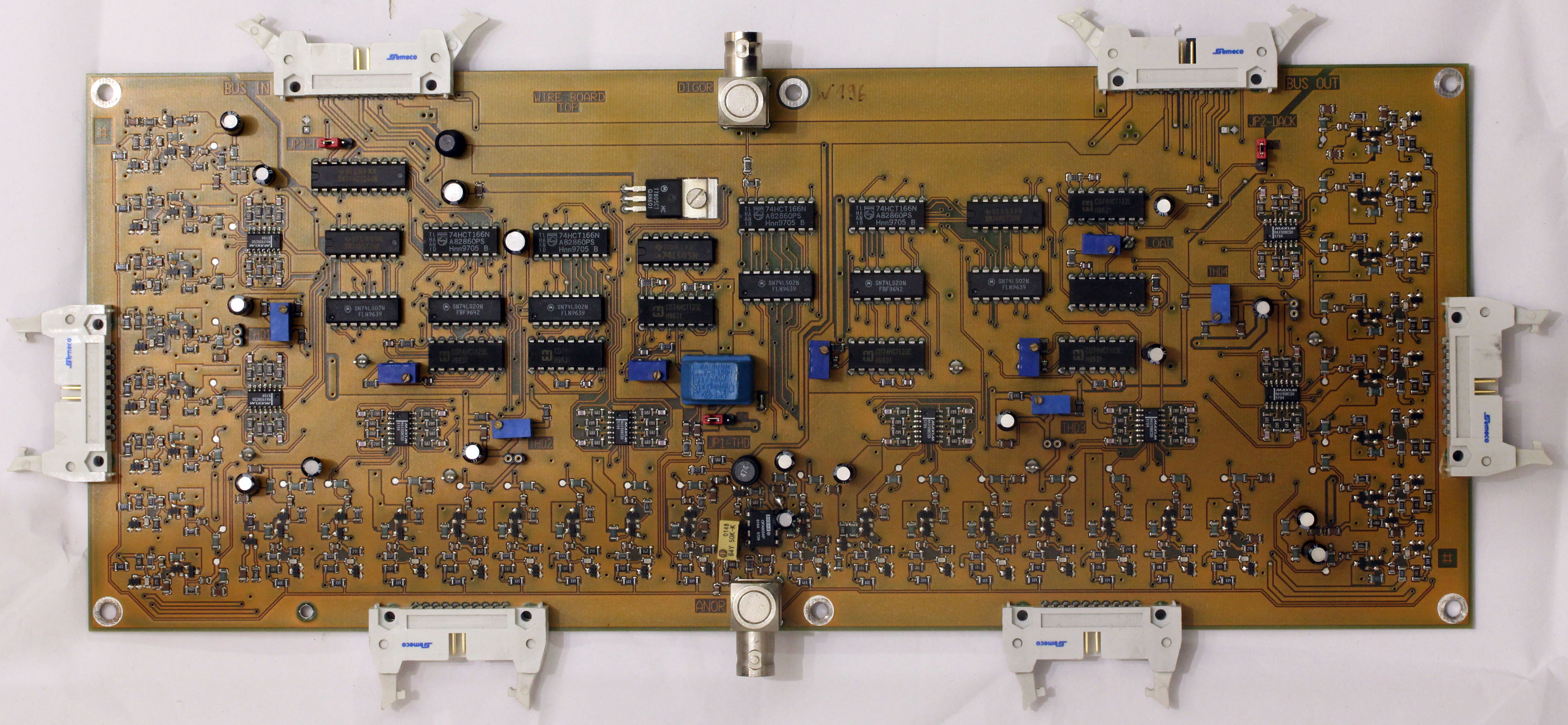
Thanks to cpresser for contributing this wonderfully photographed circuit board as this month’s entry.
Non-Destructive Silicon Imaging (and Winner of Name that Ware December 2022)
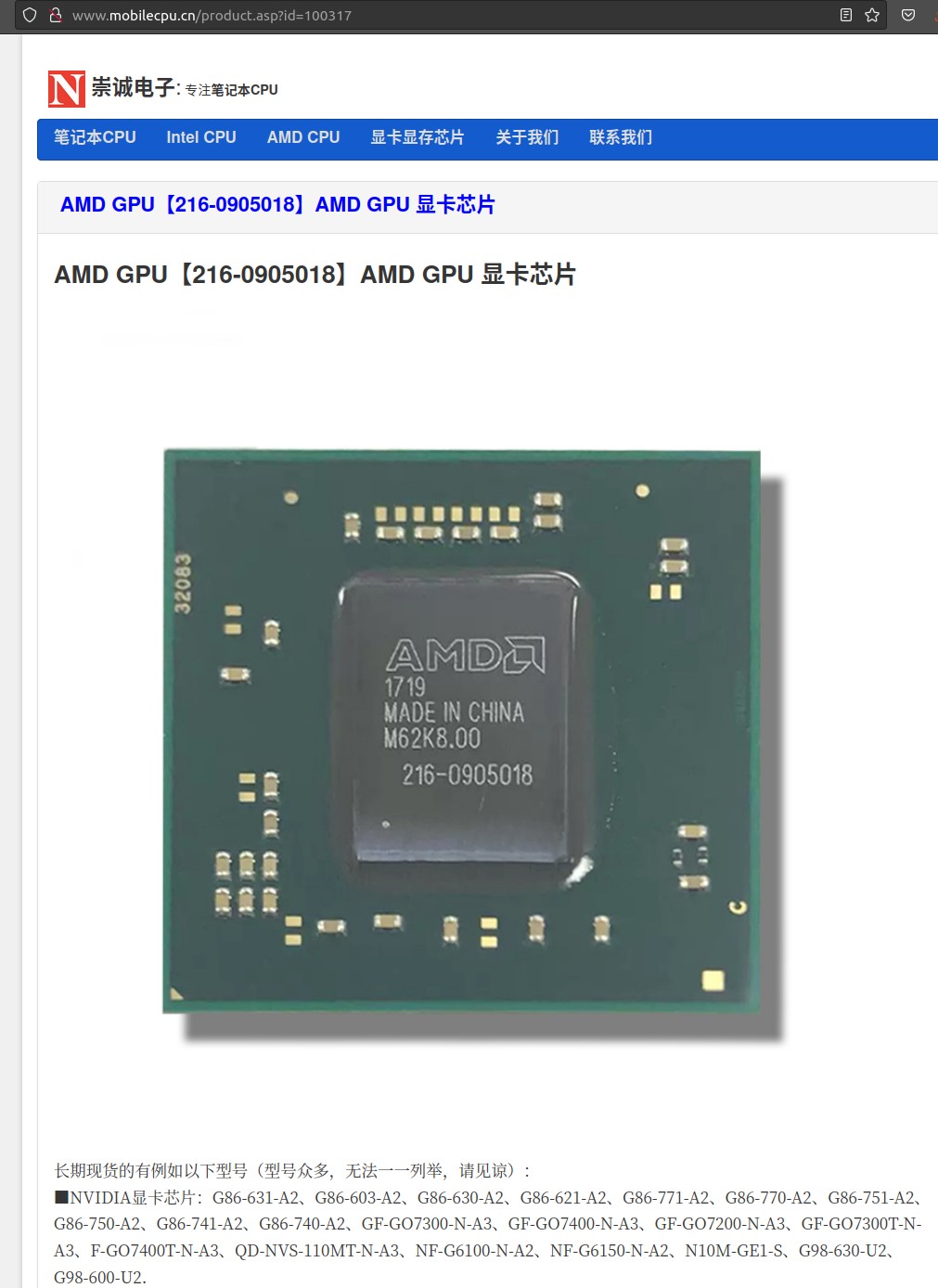
January 4th, 2023The ware for December 2022 is an AMD Radeon RX540 chip, part number 216-0905018. Congrats to SAM for guessing the ware; email me for your prize. The image is from Fritzchen Fritz’s Flickr feed; I recommend checking out his photos (or you can follow him on twitter). Even if you aren’t into photos of chips, he elevates it to an art. Even more amazingly, all of his work is public domain; hats off to him for contributing these photos to the commons with such a generous license, because it is not easy to prepare the material and take images of this quality. If any of my readers happens to know him and are willing to make an introduction, I’d appreciate that. I only discovered his work by chance while doing some background research.
First, here is the entire photo from which the ware was cropped:
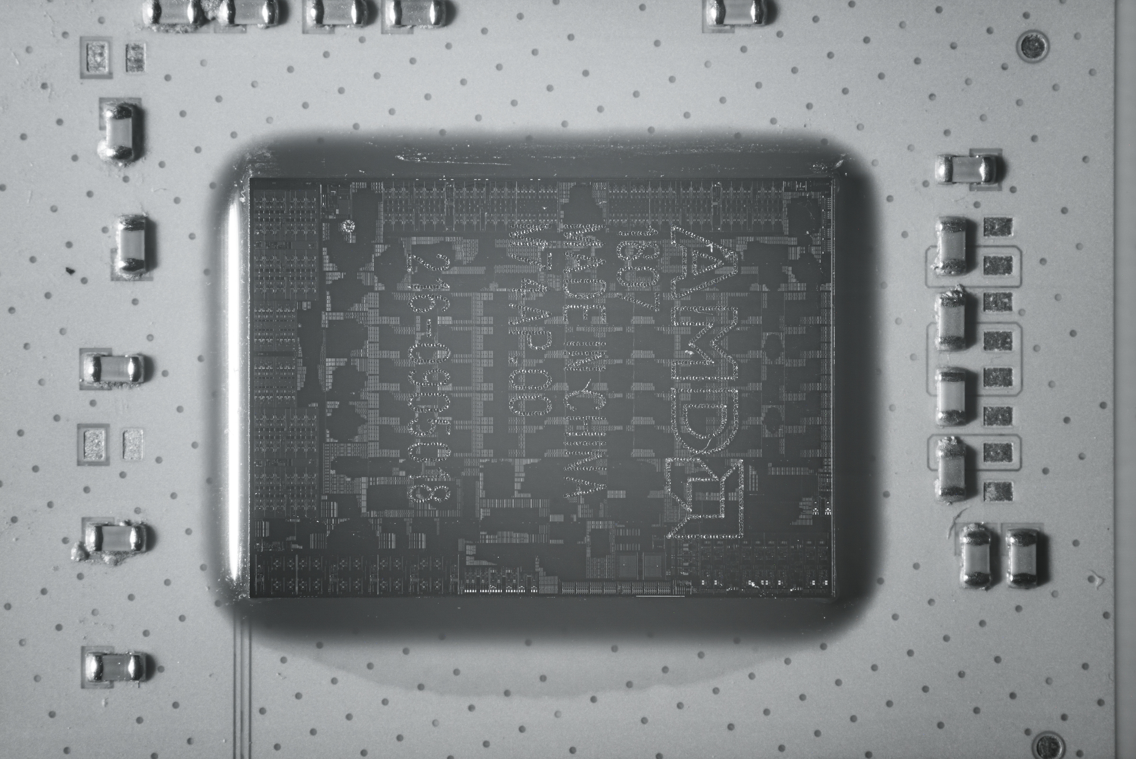
Credit: Fritzchen Fritz
Interestingly, you can see the design of the chip in this photograph. This is not photoshop; based on the notes accompanying the photo, this was taken in “NIR”, or near-infrared, using a Sony NEX-5T.
Silicon is transparent to IR, and so, photographs taken in infra-red can be used to verify, at a coarse level, the construction of a chip!
I was pretty excited to see photos like this posted on the Internet, at full-resolution, because I have only read about this technique in journal articles. Silicon becomes very transparent in infrared:
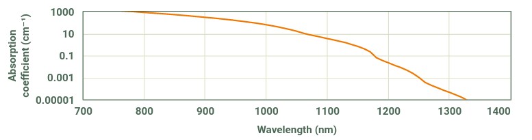
Silicon’s absorption of light in the near infrared range. A lower value is more transparent. Generated using PV lighthouse.
This principle forms the foundation of my efforts to verify the construction of silicon in a non-destructive fashion.
The line between NIR/SWIR (near/shortwave infrared) depends on who you ask, but according to Edmud Optics, it places the line at 1000nm. By this definition, I’m inferring that the above photograph was probably taken using a powerful 900nm illuminator positioned to the left of the chip near the horizon. A bright light at that wavelength would have sufficient power to penetrate the ~1mm thickness of silicon to image the circuits on the other side, and placing it near the horizon prevents swamping the sensor with reflected light except for the bits of metal that happen to catch the light and reflect it upwards.
It’s also possible to do this with a SWIR sensor, using a wavelength closer to 1300nm (where silicon is as transparent as glass is to visible light), but the resolution of the photographs are much higher than the best SWIR sensor that I’m aware of. Unfortunately, it seems all interesting technologies are regulated by the US government’s ITAR, and SWIR area-scan sensors are no exception. I’m guessing they are also a critical component of night vision gear, and thus it is hard to obtain such sensors without a license. Regardless, even the photos taken at 900nm are a powerful demonstration of the utility of IR for inspecting the construction of silicon.
Here’s another image taken using what looks like the same technique:
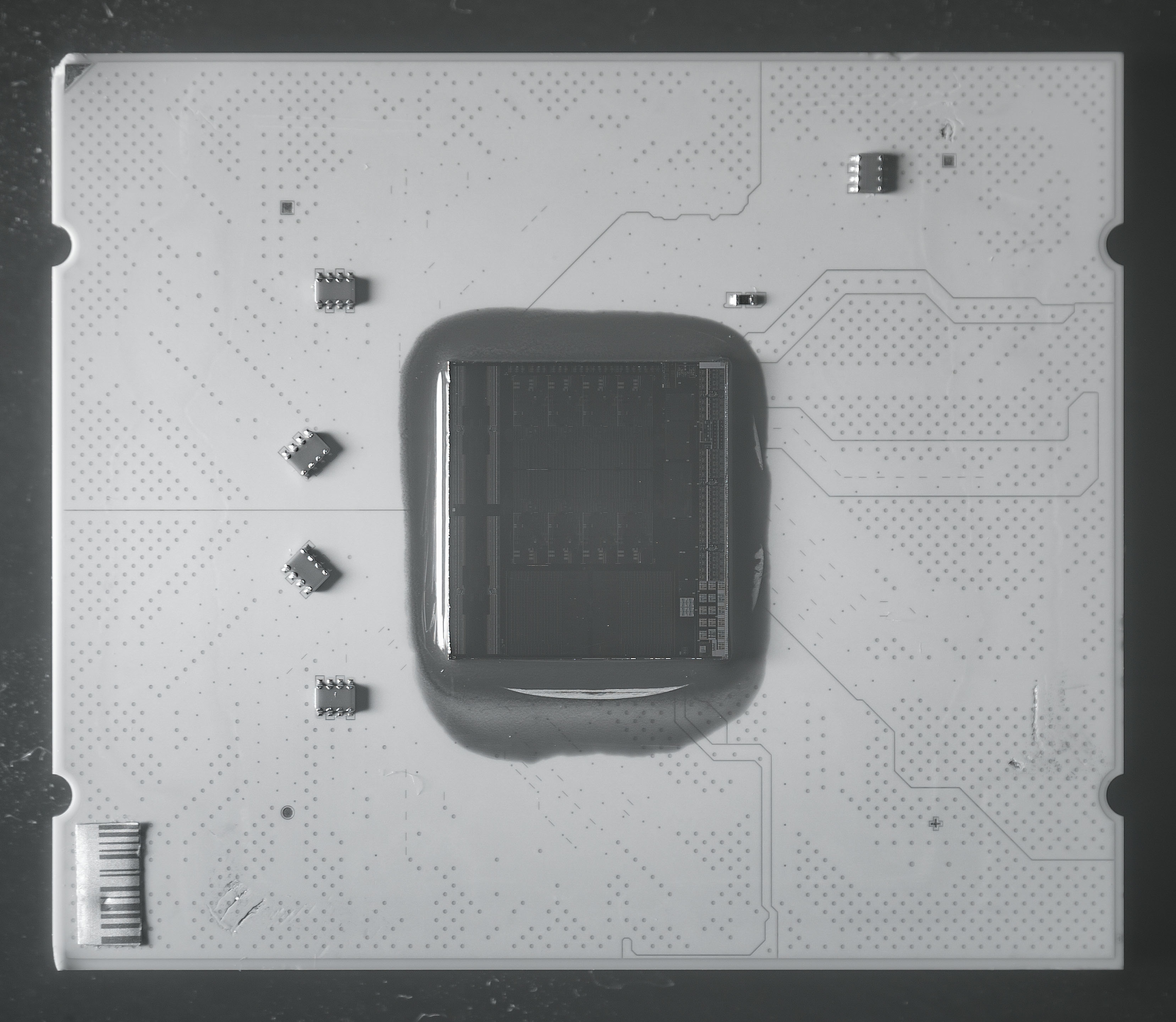
Credit: Fritzchen Fritz
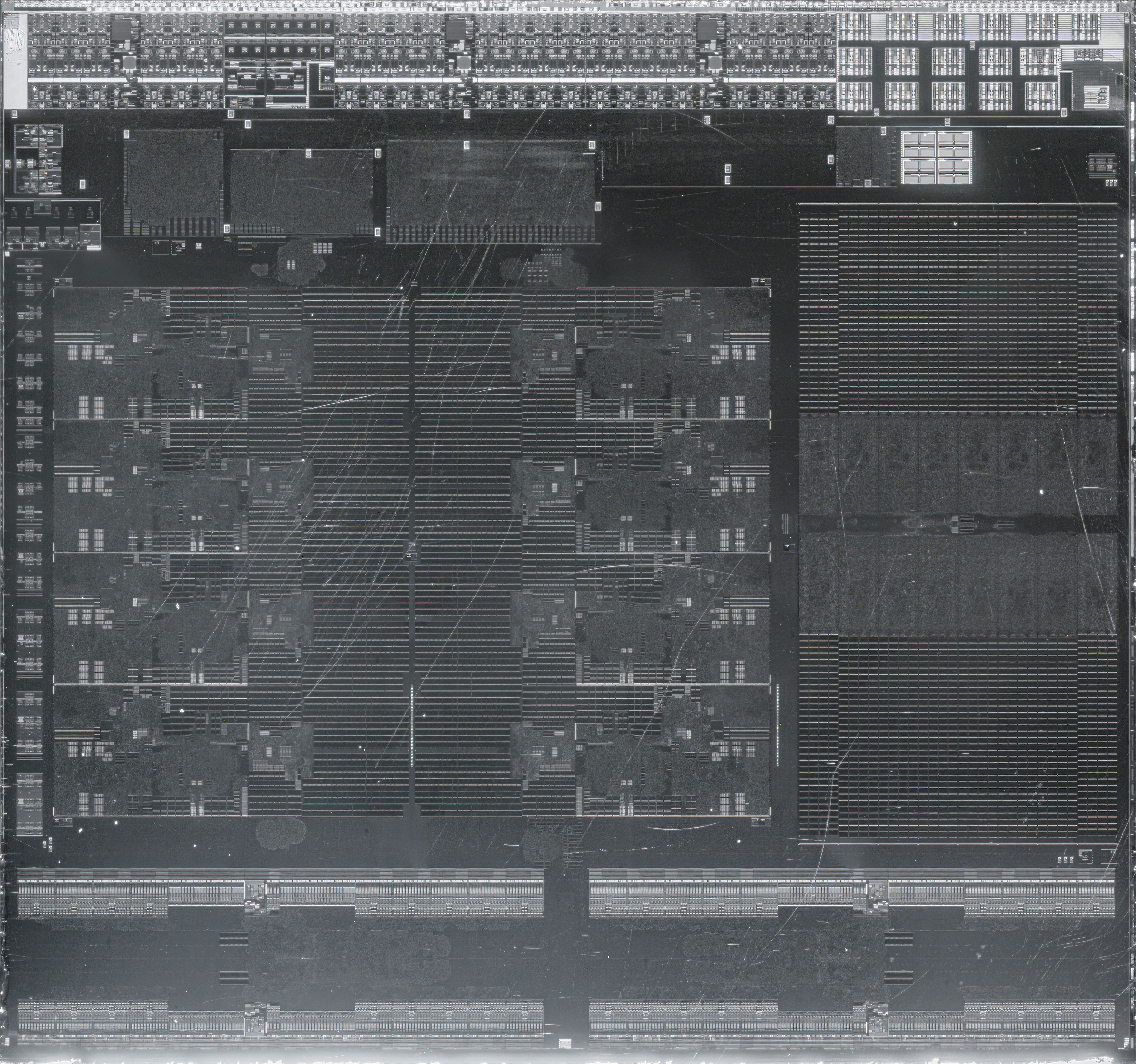
This is of the Via Centaur CHA, which has an excellently detailed Wikichip page complete with floorplans, such as the one shown below.
_annotated.png)
Credit: Wikichip
Remember, the IR image is from the back side of the die, so you have to mirror-image (and rotate) the front-side floorplan in your head to line it up with orientation of the photograph.
According to Wikichip, this is a TSMC 16FFC (16nm) process, with a 194mm^2 die area. This means the die above is about 13.9 mm on a side. The image as-is (which is 90% package and 10% die) resolves at about 18um/pixel, so perhaps if it was a die-only shot we could resolve at something close to 5um/pixel in a single image.
With image stitching, the resolution can be even higher:
Credit: Fritzchen Fritz
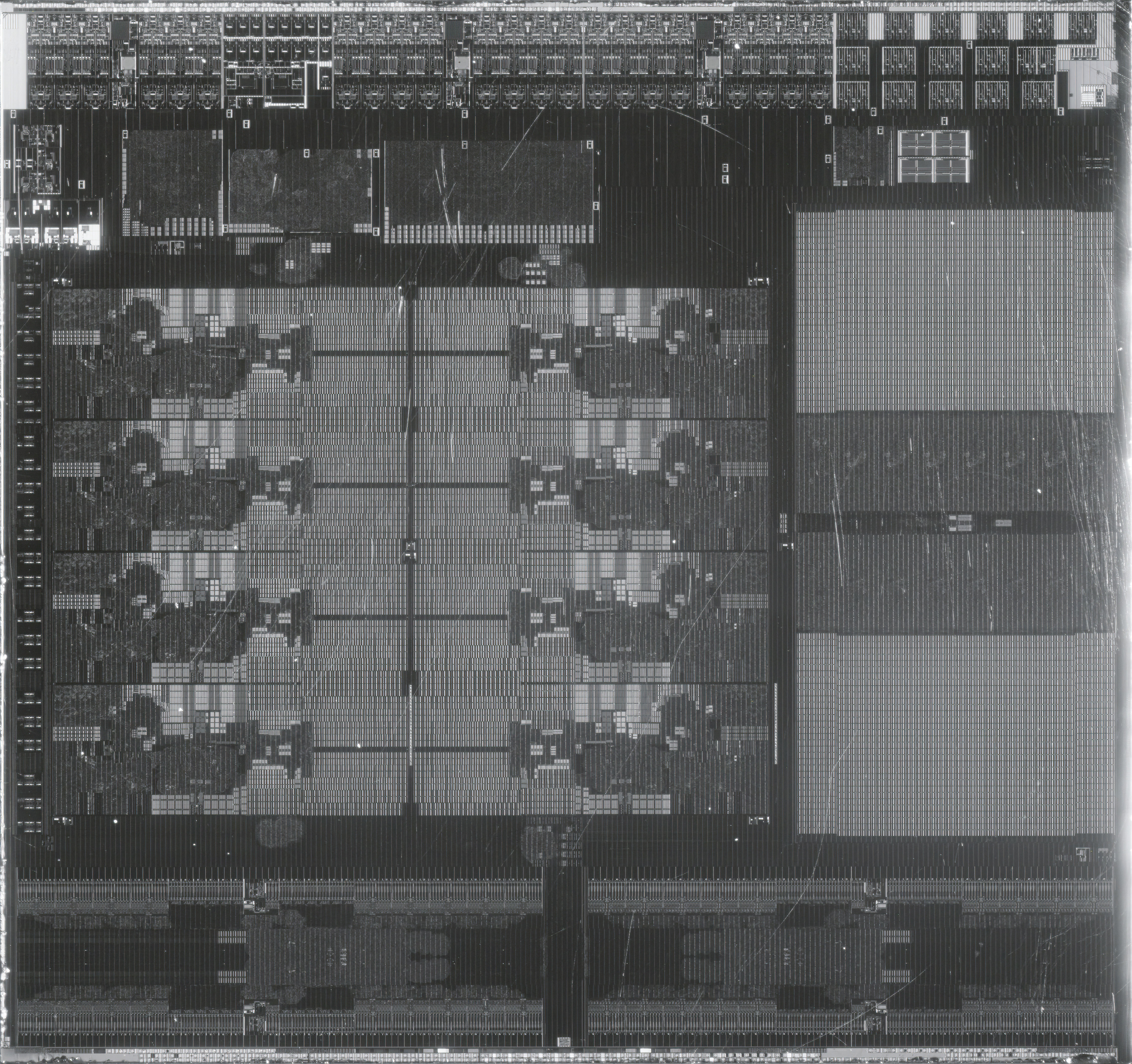
Credit: Fritzchen Fritz
In these two photos, it seems the light source was rotated 90 degrees with respect to the chip, so that different sets of components are highlighted, depending on the bias of the metal routes for that component. Note that I’m inferring this image is taken through the back side because of the presence of scratches that would be from the exposed surface of the silicon, and the orientation of the imaged die is consistent with a back-side shot.
The resolution of the above images boils down to about 3um/pixel — getting fairly close to the limit of what you can do with NIR light. To put this in perspective, TSMC 16FFC has minimum metal pitch of 64nm, so a 9-track standard cell would be 0.576um tall, and an SRAM bitcell has a size of 0.074um^2, so one pixel encompasses roughly 25 logic gates or 120 bits of SRAM. In these images, you can clearly make out variations in the density of standard cell logic, as well as the size and location of individual memory macros; the internal structure of the PCI-express drivers is also readily apparent.
I’ve been contemplating silicon supply chain attacks quite a bit, and I think that at this resolution, one can rule out the following forms of silicon supply chain attacks:
- Replacement of the chip with an entirely different design that emulates the original
- Insertion of a ROM larger than a few hundred bits containing alternate microcode or instruction codings
- Insertion of a RAM macro for recording data — probably of any practical size for a RAM macro, due to the presence of line drivers/amplifiers creating a high-signal reflection
- Insertion of extra I/O drivers
- Potential detection of extra eFuse elements
- Likely able to detect recompilation/resynthesis of standard cell blobs
This significantly constrains the types of attacks one has to worry about. Without backside imaging and just looking at the exterior package, it’s difficult to even know if a chip has been wholesale replaced for an inferior clone or an emulated version. The inability to add significant amounts of microcode ROM or RAM constrains the types of modifications one could make to a CPU and “get away with it”; with some additional design-level guard rails and open source RTL I suspect one could virtually eliminate effective CPU instruction-level modifications that doesn’t also introduce ISA-level flaws in every mode of operation that could be easily detected with a software-only test.
I have reasons to suspect that modifications to an eFuse box would be detectable, but because eFuses are carefully guarded black boxes such that even chip designers are not allowed to see their insides, it’s possible that a foundry could just build a back door into every eFuse box and we wouldn’t be able to tell the difference because it would be “normal”.
Finally, depending on the repeatability of the place/route tool, a modification to the RTL that triggers a re-synthesis and place/route could change the gross morphology of the standard cell blob. However, I’m not familiar enough with the latest industry-standard tools to know how big a difference that would create. I imagine there are ways to control the place and route seed so that results look very similar if only small changes are made to the RTL, such as inserting a patch wire on a single bit in a non-congested region of a design. However, a larger change, such as the insertion of a 64-bit sampling register in the datapath somewhere, would likely be detectable with this level of imaging.
There’s still a class of exploits that could be undetected with this level of imaging. This would include:
- Small changes to test access paths; for example, patching existing ATPG scan chain logic to an existing but unused point on an I/O mux hard macro. This could facilitate unrestricted access to internal state with some additional off-chip circuitry.
- Spare cell-only modifications that are manually patched using higher metal levels. These patches would be obscured from the back side due to masking by lower metal layers, and by definition no additional transistors are involved.
- Dopant-level attacks, where transistor flavor or threshold voltages are modified, perhaps to bias a random number generator or to modify the function of a single gate.
- Other careful modifications that disturb fewer than ~100 logic gates or ~100 bits of SRAM.
However, the attack surface of concern is by far smaller with this level of imaging than the current state-of-practice, which consists of squinting at the top markings on a chip package.
My hope for supply chain verification is that end users can establish a practical amount of trust in silicon chips through a combination of imaging and design analysis, without requiring a fully-open PDK (although it certainly is easier and better if the PDK is open). The missing link is an automated imager that can produce results similar to the ones demonstrated by Fritzchens Fritz. These images can then be compared against die shots released by the designer. These die shots would be low enough resolution to not violate foundry NDA, but still have enough detail to constrain the intended positions of blocks. The remaining verification gap (on the order of hundreds of gates / hundreds of bits of SRAM) could be filled in with design techniques that harden against small exploit vectors, perhaps by the use of redundant/byzantine fault tolerant logic, or by some combination of inducing faults and scan chain analysis to confirm correct construction at the gate level. And finally, open source RTL is required to help establish a link between what is visible, and what was intended by the designer (and of course also to help discover any bugs/backdoors introduced by the designer).
And now back to the Name that Ware competition. Confusingly, one of the first answers in the comments points to a tweet that also claims to have taken the photo. I did a bit of poking about and the image appears to be identical to the one on Fritzchen Fritz’s feed, down to the position of solder particulates and lint. There’s a number of possible explanations for this; I won’t speculate as to what is going on, but I will comment that the chip is not typically referred to as an “AMD M74AP” — M74AP is the lot code, so I couldn’t declare Taylan the winner, unfortunately (so close, though!). 216-0905018 is the canonical part number; if you search around for the part number, you will see several examples of chips that have the same part number, but a different lot code. This one, for example, has a lot code of M62K8.00.
Postscript
When going through Fitzchen Fritz’s photos, I was also considering using this image as the Name that Ware:
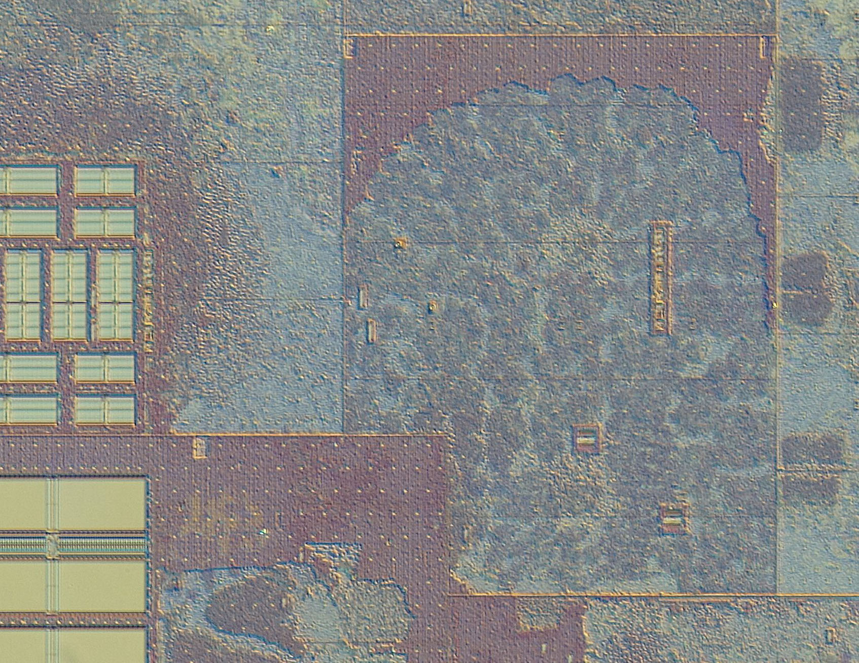
Credit: Fritzchen Fritz
It’s a tiny portion (1/400th the area) of an Intel i3-8121U (187MiB full-res mirror link), fabbed in a 10nm process. The region is cropped from a section centered in the top right quadrant of the image.
In terms of actual dimensions, the region is about 485um x 375um if I’ve done my math right – about the area covered by a medium sand particle. According to Wikichip, a 9-track standard cell would be 0.324um high, so if the area were covered with nothing but square 9-track standard cells, it would hold 1500 x 1150 cells (1.7M cells, or about one gate per pixel in the photo), or 700kiB of the densest SRAM cells (without sense amps etc.)
However, the area is not homogeneously covered with one or the other, and in fact has lots of unused silicon. The darker purplish regions are unused silicon — for one reason or the other (often times routing/floorplanning constraints, and sometimes schedule constraints), there are no logic transistors there. I think only the solid tan regions in the lower left hand corners contain high density SRAM cells; the smaller rectangles above them could contain SRAM, but could also be some other type of memory more optimized for performance or port count.
Each SRAM region is divided by sense amps and other driver logic. One solid, SRAM-cell-only region is about 48.7×28.7um, which is about 5.4kiB, so the overall region of larger rectangles holds about 22kiB of memory, including an overhead of about 35% for the drivers and amps. Likewise, the cauliflower-like structure in the center is about 750 gates wide by 900 gates high (if the gates were square — which they aren’t, so this is an upper bound), or about 600k gates (again, this image is at a resolution of about 1 pixel/gate). That would fit about a dozen VexRiscv cores, or a few 80486’s, so it’s not a small chunk of logic.
Finally, I think (but am not sure) that the rectangular cut-out regions within the cauliflower-region are clock drivers or repeaters. No transistors are placed in the trench around them probably to meet thermal flux constraints, and I also wouldn’t be surprised if they packed some local decoupling capacitors around the drivers using dummy transistors and/or MIM capacitors to reduce power droop and induced jitter in that region.
What I love about this image is how clouds of standard cells take on organic shapes when viewed at this resolution. To me it looks more like mold or bacteria growing in a petri dish than the pinnacle of precision manufactured goods. But perhaps this is just convergent evolution in action, driven by the laws of physics: signals diffuse through on-chip wires, much like nutrients in a media.
Name that Ware, December 2022
December 31st, 2022The Ware for December 2022 is shown below.
Turning this into a suitable Name that Ware-style entry was a bit tough, but I think maybe I hit a balance between leaving enough clues, and giving it away. We’ll see shortly!
I have a lot more to say about this ware: I will give proper attribution once the ware has been guessed (or the end of the month, whichever is sooner); but let’s just say I was incredibly pleased to find such detailed images in the public domain.
Winner, Name that Ware November 2022
December 31st, 2022The ware for November 2022 is a Keithley 2110-240. I’ll give Rodrigo F. the win, but I’m curious how he knew it was the -240 version; I did not expect someone to discern the line voltage rating from the photos!
Also, thank you Ian Mason for the lucid explanation of the exposed traces near key signals. Here’s his quoted answer, so you don’t have to look it up in the comment thread:
The reason for stripping resist from over guard rings [is] to ensure that any leakage paths come into electrical contact with the guard ring. If you had, say, a bit of flux residue as a leakage path, if it passed between two pins but over the solder mask then the guard ring would be insulated from it and would have no effect. The whole point of a guard ring is that it’s a (relatively) low impedance path either to ground or to a duplicate of the measured signal – being insulated behind soldermask is anything but low impedance.
It’s tricks like these they never teach you in school. I’m guessing it was a hard-learned lesson for the persons who had to figure out that trick on their own. Thanks for sharing the knowledge!
Edit: I forgot to note that Rodrigo F. should email me to claim the prize!
