It’s been four months since we finished Novena’s crowd funding campaign, and we’ve made a lot of progress since then. Since then, a team of people have been hard at work to make Novena a reality.
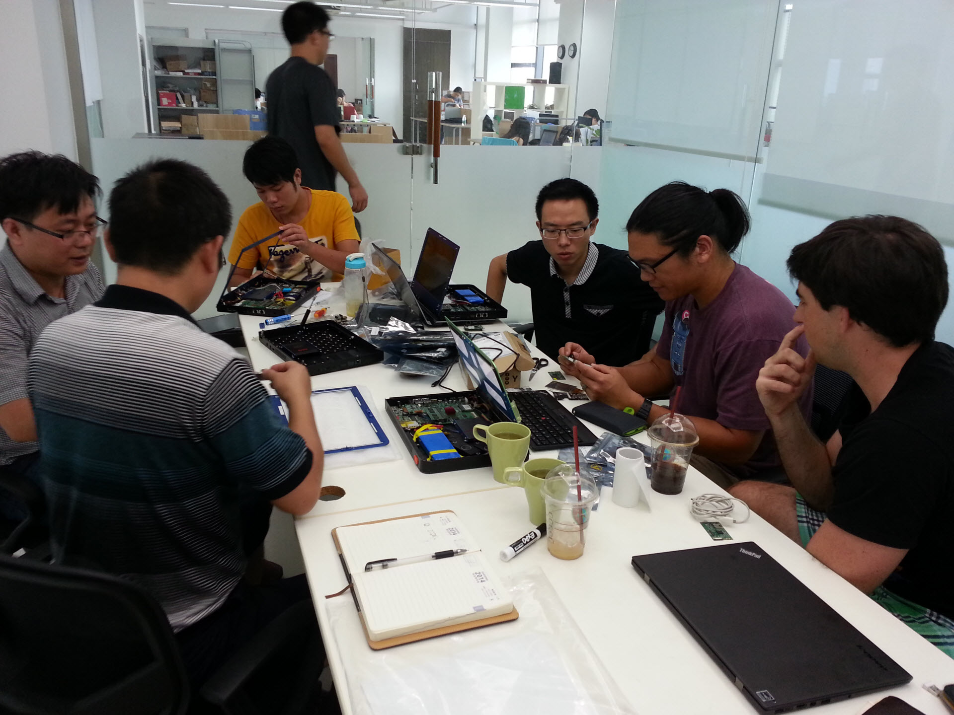
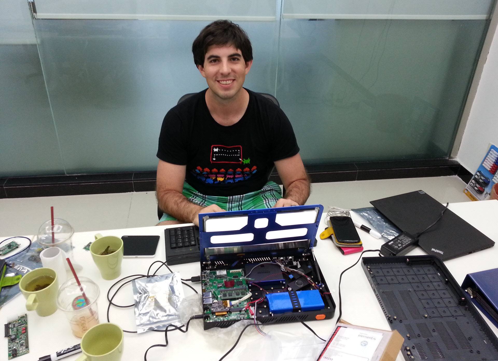
It takes many hands to build a product of this complexity, and we couldn’t do it without our dedicated and hard-working team at AQS. Above is a photo from the conference room where we did the T1 plastics review in Dongguan, China.
In this update, we’ll be discussing progress on the Casing, Electronics, Accessories, Firmware and the Community.
Case construction update
We’re very excited that the Novena cases we’re carrying around are now made of entirely production-process hardware — no more prototypes. A total of 10 injection molding tools, many of the family molds, have been opened so far; for comparison, a product like NeTV or chumby had perhaps 3-4 tools.
For those not familiar with injection molding, it’s a process whereby plastic is molded into a net shape from hot, high pressure liquid plastic forced into a cavity made out of hardened steel. The steel tool is a masterpiece of engineering in itself – it’s a water-cooled block weighing in at about a ton, capable of handling pressures found at the bottom of the Mariana Trench, and the internal surfaces are machined to tolerances better than the width of a human hair. And on top of that, it contains a clockwork of moving pieces, with dozens of ejector pins, sliders, lifters and parting surfaces coming apart and back together again smoothly over thousands of cycles. It’s amazing that these tools can be crafted in a couple of months, yet here we are.
With so much complexity involved, it’s no surprise that the tools require several iterations of refinement to get absolutely perfect. In tooling jargon, the iterations are referred to as T0, T1, T2…etc. You’re doing pretty good if you can go to full production at T2; we’re currently at T1 stage. The T1 plastics are 99% there, with a few issues relating to flow and knit lines, as well as a couple of spots where the plastic is warping during cooling or binding to the tool during ejection and causing some deformation. This manifests itself in a couple spots where the seams aren’t as tight as we’d like them to be in the case.
Most people have only seen products of finished tooling, so I thought I’d share what a pretty typical T0 shot looks like, particularly for a large and complex tool like the Novena case base part. Test shots like this are typically done in colors that highlight defects and/or the resin is available as scrap, hence the gray color. The final units will be black.
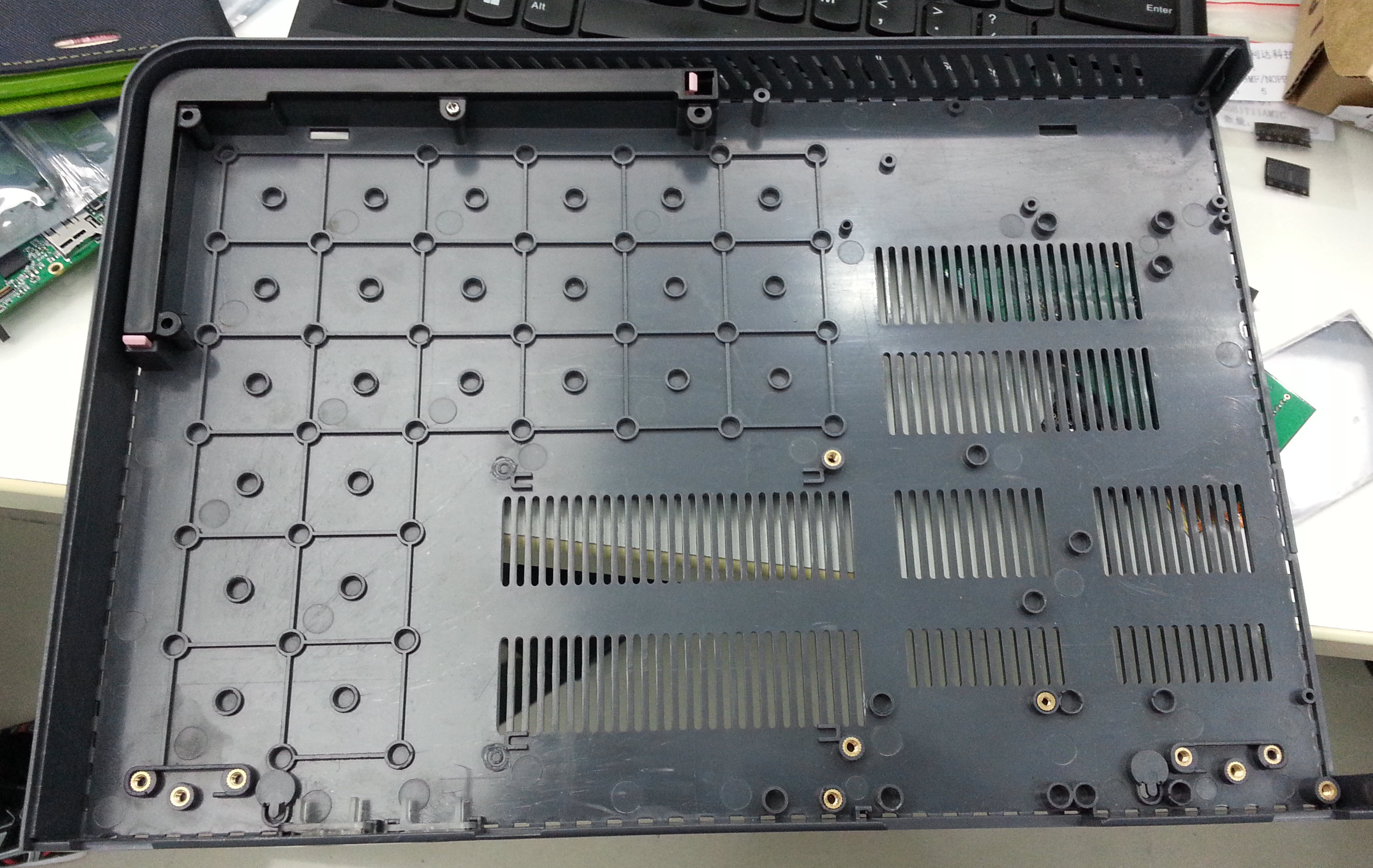
There’s a lot going on with this piece of plastic, so below is a visual guide to some of the artifacts.

In the green boxes are a set of “sink marks”. These happen when the opposite side of the plastic has a particularly thin or thick feature. These areas will cool faster or slower than the bulk of the plastic, causing these regions to pucker slightly and cause what looks like a bit of a shadow. It’s particularly noticeable on mirror-finish parts. In this case, the sink marks are due to the plastic underneath the nut bosses of the Peek array being much thinner than the surrounding plastic. The fix to this problem was to slightly thicken that region, reducing the overall internal clearance of the case by 0.8mm. Fortunately, I had designed in a little extra clearance margin to the case so this was possible.
The red arrow points to a “knit line”. This is a region where plastic flow meets within the tool. Plastic, as it is injected into the cavity, will tend to flow from one or more gates, and where the molten plastic meets itself, it will leave a hairline scar. It’s often located at points of symmetry between the gates where the plastic is injected (on this tool, there are four gates located underneath the spot where the rubber feet go — gates are considered cosmetically unattractive and thus they are strategically placed to hide their location).
The white feathery artifacts, as indicated by the orange arrow, are flow marks. In this case, it seems plastic was cooling a bit too quickly within the tool, causing these streaks. This problem can often be fixed by adjusting the injection pressure, cycle length, and temperature. This tweaking is done using test shots on the molding machine, with one parameter at a time tweaked, shot after shot, until its optimum point is found. This process can sometimes take hundreds of shots, creating a small hill of scrap plastic as a by-product.
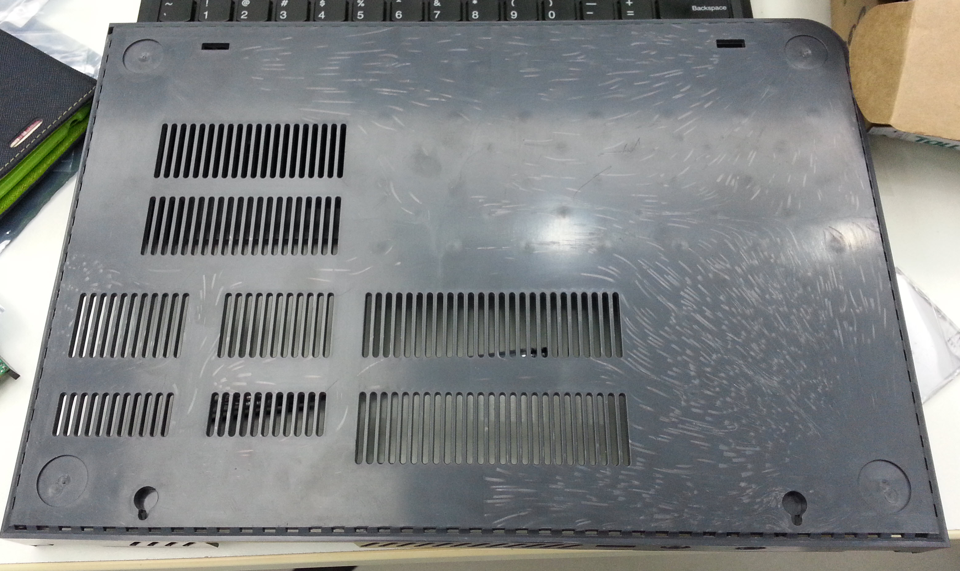
Most of these gross defects were fixed by T1, and the plastic now looks much closer to production-grade (and the color is now black). Below is the T1 shot in initial testing after transferring live hardware into the plastics.
There’s still a few issues around fit and finish. The rear lip is binding to the tool slightly during ejection, which is causing a little bit of deformation. Also, the panel we added at the last minute to accommodate oversized expansion boards isn’t mating as tightly as we’d like it to. But, despite all of these issues, the case feels much more solid than the prototypes, and the gas piston mechanism is finally consistent and really smooth.
Front bezel update
The front bezel of Novena’s case (not to be confused with the aluminum LCD bezel) has gone through a couple of changes since the campaign. When we closed funding, it had two outward-facing USB ports and one switch. Now, it has two switches and one outward-facing USB port and one inward-facing USB port.
One switch is for power — it goes directly to the power board and thus can be used to turn the system on and off even when the main board is fully powered down.
The other switch is wired to a user key press, and the intent is to facilitate Bluetooth association for keyboards that are being stupid. It seems some keyboards can take up to a half-minute to cycle through — something (presumably, it’s trying to be secure) — before they connect. There are hacks you can do to bypass that, but it requires you to run a script on the host, and the idea is by pressing this button users can trigger a convenience script to get past the utter folly of Bluetooth. This switch also doubles as a wake-up button for when the system is in suspend.
As for the USB ports, there are still four ports total in the design, but the configuration is now as follows:
In other words, we face one USB port toward the inside of the machine; since half the fun of Novena is modding the hardware, we figure making a USB port available on the inside is at least as useful as making it available on the outside.
For those who don’t do hardware mods, it’s also a fine place to plug small dongles that you generally keep permanently attached, such as a radio transceiver for your keyboard. It’s a little inconvenient to initially plug in the dongle, but keeping the radio transceiver dongle facing the inside helps protect it from damage when you throw your laptop into your travel bag.
Speakers
We toyed with several iterations of speaker selection for Novena. One of the core ideas behind the design was to make speaker choice something every user would be encouraged to make on their own. One driving reason for this is some people really listen to music on their laptop when they travel, but others simply rely upon the speaker for notification tones and would prefer to use headphones for media capabilities.
Physics dictates that high-quality sound requires a certain amount of space and mass, and so users who have a more relaxed fidelity requirement should be able to reclaim the space and weight that nicer speakers would require.
Kurt Mottweiler, the designer of the Heirloom model, had selected a nice but very compact off-the-shelf speaker, the PUI ASE06008MR-LW150-R, for the Heirloom. We evaluated that in the context of the standard Novena model and found that it fit well into the Peek Array and it also had acceptable fidelity, particularly for its size. And so, we adopted this as the standard offering for audio. However, it will be provided with a mounting kit that allows for easy removal so users who need to reclaim the space they take, or who want to go the other way and put in larger speakers, can do so with ease.
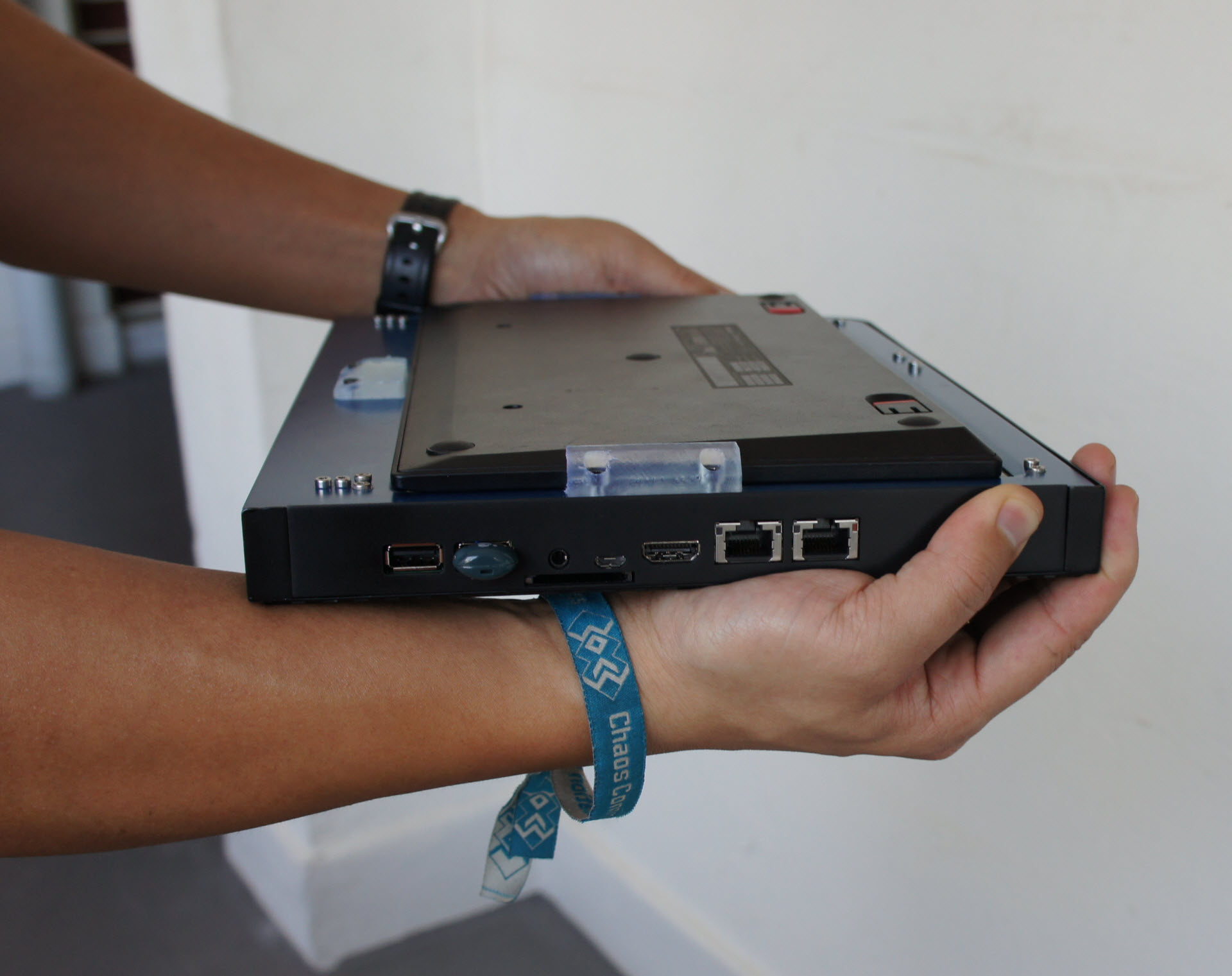
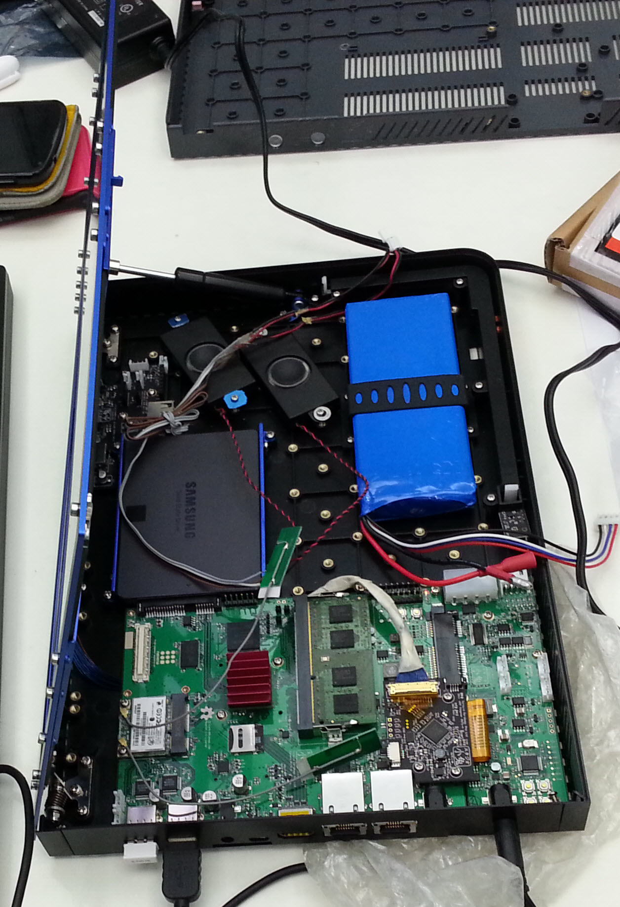
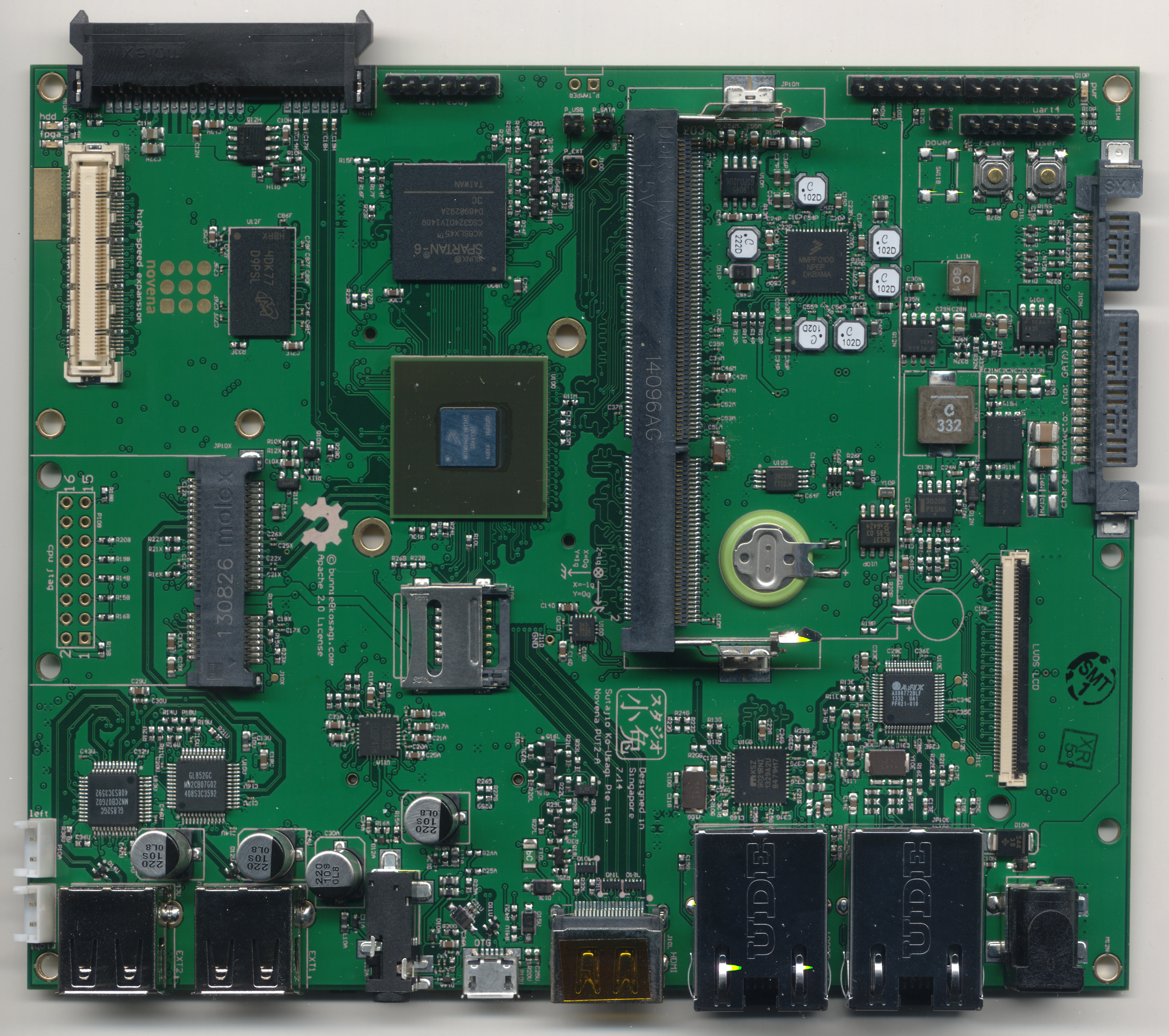
PVT2 Mainboard
The Novena mainboard went through a minor revision prior to mass production. The 21-point change list can be viewed here; the majority of the changes focused on replacing or updating components that were at risk of EOL. The two most significant changes from a design standpoint were the addition of an internal FPC header to connect to the front bezel cluster, and a dedicated hardware RTC module.
The internal FPC header was added to improve the routing of signals from the mainboard to the front bezel cluster. We had to run two USB ports, plus a smattering of GPIOs and power to the front bezel and the original scheme required multiple cables to execute the connection. The updated design condenses all of this into a single FPC, thereby simplifying the design and improving reliability.
A dedicated hardware RTC module was added because we couldn’t get the RTC built into the i.MX6 to perform well. It seems that the CPU simply had a higher leakage on the RTC than reported in the datasheet, and thus the lifetime of the RTC when the system was turned off was measured in, at best, minutes. We made the call that there was too much risk in continuing to develop with the on-board RTC and opted to include an external, dedicated RTC module that we knew would work. In order to increase compatibility with other i.MX6 platforms, we picked the same module used by the Solid-Run Hummingboard, the NXP PCF8523T/1.

GPBB
The GPBB got a face-lift and a couple of small mods to make it more hacker-friendly.
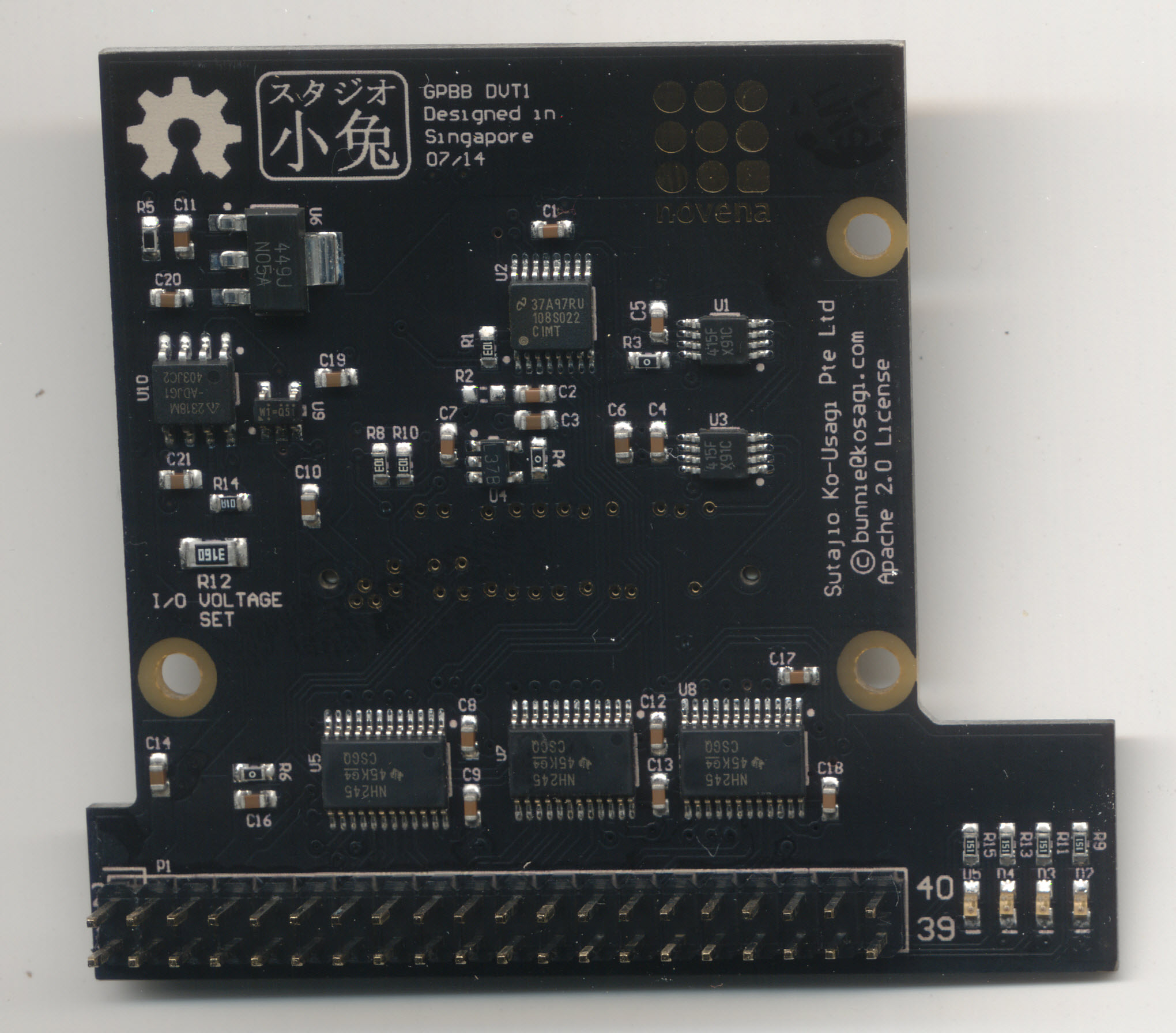
I think everything looks a little bit nicer in matte black, so where it doesn’t compromise production integrity we opted to use a matte black soldermask with gold finish.
Beyond the obvious cosmetic change, the GPBB also features an adjustable I/O voltage for the digital outputs. The design change is still going through testing, but the concept is to by default allow a 5V/3.3V selectable setting in software. However, the lower voltage can also be adjusted to 2.5V and 1.8V by changing a single resistor (R12), which I also labelled “I/O VOLTAGE SET” and made a 1206 part so soldering novices can make the change themselves.
In our experience, we’re finding an ever-increasing gulf between the voltage standards used by hobbyists and what we’re actually finding inside equipment we need to reverse engineer; and thus, to accommodate both applications a flexible voltage output selection mechanism was added to the GPBB.
Desktop Passthrough
The desktop case originally included just the Novena mainboard, and the front panel breakout. It turns out this makes power management awkward, as the overall power management system for the case was designed with the assumption there is a helper microcontroller managing a master cut-off switch.
Complexity is the devil, and it’s been hard enough to get the software going for even a single configuration. So in net we found it would be cheaper to introduce a new piece of hardware rather than deal with multiple code configurations.
Therefore, desktop systems are now getting a power pass-through board as part of the offering. It’s a simple PCBA that contains just the STM32 controller and power switch of the full Senoko board. This allows us to use a consistent gross power management architecture across both the desktop and the laptop systems.
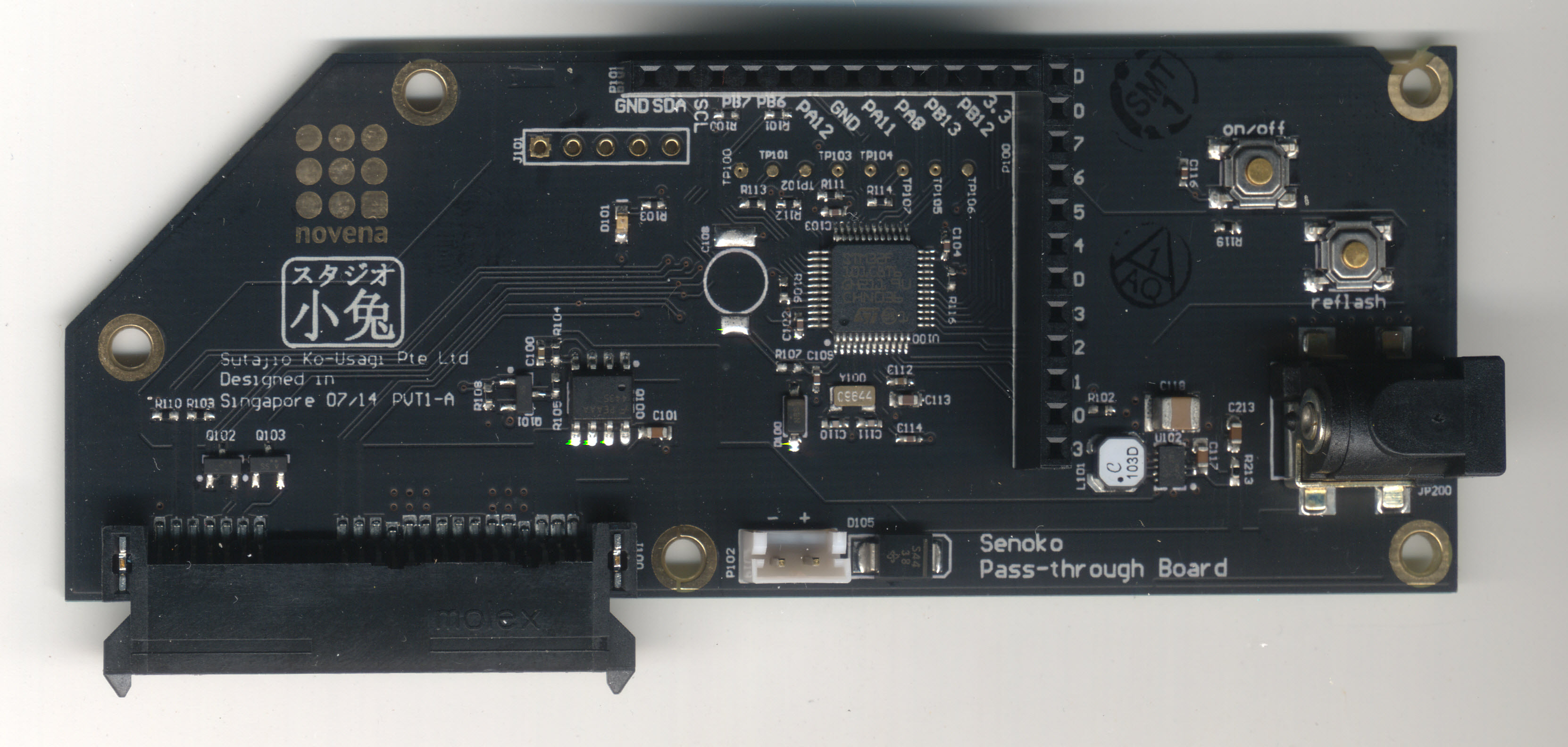
Of course, this is swatting a fly with a sledgehammer, but this sledgehammer costs as much as the flyswatter and it’s inconvenient to carry both a fly swatter and a sledgehammer around. And so yes, we’re using a 32-bit ARM CPU to read the state of a pushbutton and flip a GPIO, and yes, this is all done using a full multi-threaded real time operating system (ChibiOS) running underneath it. It feels a little silly, which is why we broke out some of the unused GPIOs so there’s a chance some clever user might find an application for all that untapped power.
Battery
The battery pack for Novena is and will continue to be a wildcard in the stack. It’s our first time building a system with such a high-capacity battery, and working through all the shipping regulations to get these delivered to your front door will be a challenge.
Some countries are particularly difficult in terms of their regulations around the importation of lithium batteries. In the worst case, we’ll send your laptop with no battery inside, and we will ship separately, at our cost, an off-the-shelf battery pack from a vendor that specializes in RC battery packs (e.g. Hobby King). You will have the same battery we featured in the crowd funding campaign, but you’ll need to plug it in yourself. We consider this to be a safe fall-back solution, since Hobby King ships thousands of battery packs a day all around the world.
However, this did not stop us from developing a custom battery pack. As it’s very difficult to maintain a standing stock of battery packs (they need to be periodically conditioned), we’re including this custom battery pack only to backers of the campaign, providing their country of residence allows its import (and we won’t know for sure until we try). We did get UN38.3 certification for the custom battery pack, which in theory allows it to be shipped by air freight, but regulations around this are in flux. It seems countries and carriers keep on inventing new rules, particularly with all the paranoia about the potential use of lithium batteries as incendiary devices, and we don’t have the resources to keep up with the zeitgeist.
For those who live in countries that allow the importation of our custom pack, the new pack features a 5000mAh rated capacity (about 2x the capacity over the pack we featured in the crowd campaign, which had 3000mAh printed on the outside but actually delivered about 2500mAh in practice). In real-life testing, the custom pack is getting about 6-7 hours of runtime with minimal power management enabled. Also, since I got to specify the battery, I know this one has the correct protection circuitry built into it, and I know the provenance of its cells and so I have a little more confidence in its long-term performance and stability.
Of course, it’s a whole different matter convincing the lawmakers, customs authorities, and regulatory authorities of those facts…but fear not, even if they won’t accept this custom limited-edition battery, you will still get the original off-the-shelf pack promised in the campaign.
Hard Drive
In the campaign, we referenced providing 240GiB Intel 530 (or equivalent) and 480GiB Intel 720 drives for the laptop and heirloom models, respectively. We left the spec slightly ambiguous because the SSD market moves quickly, and probably the best drive last February when we drew up the spec will be different from the best drive we could get in October, when we actually do the purchasing.
After doing some research, it’s our belief that the best equivalent drives today are the 240GiB Samsung 840 EVO (for the laptop model) and the 512GiB Samsung 850 Pro (for the Heirloom). We’ve been personally using the 840 EVO in our units for several months now, and they have performed admirably. An important metric for us is how well the drives hold up under unexpected power outages — this happens fairly often, for example, when you’re doing development work on the power management subsystem. Some hard drives, such as the SanDisk Extreme II, fail quite reliably (how’s that for an oxymoron) after a few unexpected power-down cycles. We’ve also had bad luck with OCZ and Crucial drives in the past.
Intel drives have generally been pretty good, except that Intel stopped doing their own controllers for the 520 and 530 series and instead started using SandForce controllers, which in my opinion removes any potential advantage they could have being both the maker of the memory chips and the maker of the controller. The details of how flash memory performs, degrades, and yields are extremely process-specific, and at least in my fantasy world a company that produces flash + controller combinations should have an advantage over companies that have to mix-and-match multiple flash types with a semi-generic controller. Furthermore, while the Intel 720 does use their home-grown controller solution, it’s a power hog (over 5W active power) and requires a 12V rail, and is thus not suitable for use in laptop environments.
The 840 EVO series comes with a reasonable 3-year warranty and at it’s held up well against one site’s write endurance test. After using mine for several months, I’ve had no complaints about it, and I think it’s a solid every-day use drive for firmware development. We also have a web server that hosts most of the media content for this and a couple other blogs, wikis, and bug tracking tools, and it’s a Novena running off an 840 EVO.
For the premium Heirloom users, we’re very excited to build in the 850 PRO series. This drive comes with a serious warranty that matches the “heirloom” name — 10 years. The reason behind their ability to offer such a high claim of reliability is even more remarkable. The drive uses a technology that Samsung has branded “V-NAND”, which I consider to be the first bona-fide production-grade 3D transistor technology. Intel claims they make 3D transistors, but that’s just marketing hype — yes, the gate region has a raised surface topology, but you still only get a single layer of devices. From a design standpoint you’re still working with a 2D graph of devices. It’s like calling Braille a revolutionary 3D printing technology. The should have stuck with what I consider to be the “original” (and more descriptive/less misleading) name, FinFET, because by calling these 3D transistors I don’t know what they’re going to call actual 3D arrays of transistors, if they ever get around to making them.
Chipworks did an excellent initial analysis of Samsung’s V-NAND technology and you can see from this SEM image they published that V-NAND isn’t about stacking just a couple transistors, Samsung is shipping a full-on 38-layer sandwich:

This isn’t some lame Intel-style bra-padding exercise. This is full-on process technology bad-assery at its finest. This is Neo decoding the Matrix. This is Mal shooting first. It’s a stack of almost 40 individual, active transistors in a single spot. It’s a game changer, and it’s not vapor ware. Heirloom backers will get a laptop with over 4 trillion of these transistors packed inside, and it will be awesome.
Sorry, I get excited about these kinds of things.
Firmware
From the software side, we’re working on finalizing the kernel, bootloader, and distro selection, as well as deciding what you’ll see when you first power on Novena.
Marek Vasut is working on getting Novena supported in mainline U-Boot, which involves a surprising number of patches. Few ARM boards support as much RAM as Novena, so some support patches were needed first. Full support is in progress, including USB and video.
We intend to ship with a mainline kernel, but interestingly Jon Nettleson has a 3.14 long-term-support kernel that is a hybrid of Freescale’s chip-specific patches combined with many backported upstream patches. Users may be interested in using this kernel over the upstream one, which has better support for thermal events and for power management.
While we prefer to go with an upstream kernel, and to get our changes pushed into mainline, other users might find this kernel’s interesting blend of community and vendor code to satisfy their needs better.
The kernel that we’ll use has most of the important parts upstreamed, including the audio chip which should be part of the 3.17 kernel. We’re still carrying a few local patches for various reasons ranging from specialized hacks to experimental features, or features that are not yet ready to push upstream, or rely on other features that are not yet upstream.
For example, the display system on a laptop is very different from what is usually found on an ARM device, and we have local patches to fix this up. In most ARM devices, the screen is fixed during boot and it isn’t possible to hot-swap displays at runtime. Novena supports two different displays at once, and allows you to plug in an HDMI monitor without needing to reboot.
Speaking of displays, the community has been hard at work on an accelerated 2D Xorg DDX driver. 2D acceleration is important, because most of the time users are interacting with the desktop, and 2D hardware uses significantly less power than 3D hardware. On a desktop machine, the 3D chip is used to composite the desktop. On Novena, which doesn’t have a fan and a small overall active power footprint, saving power is very important. By taking advantage of the 2D-only hardware, we save power while having a smoother experience. There are a few bugs that remain with the 2D driver, but it should be ready by the time we ship.
There is a 3D driver that is in progress as well. It’s able to run Quake 3 on the framebuffer, but still has to be integrated into an OpenGL ES driver before it works under X.
We’ve also been working on getting a root filesystem setup. This includes deciding which packages are installed, and customizing the list of software repositories. We want to add a repository for our kernel and bootloader, as well as for various packages which haven’t made it upstream such as an imx6 version of irqbalance. This will allow us to provide you with updated kernels as we add more support.
Finally, the question remains of what you’ll see when you first power it up. In Linux, it’s not at all common to have a first-boot setup screen where you create your user, set the time, and configure the network. That’s common in Windows and OS X, which come preinstalled, but under Linux that’s generally taken care of by the installer. As we mull the topic, we’re torn between creating a good desktop-style experience vs. making a practical embedded developer’s experience. A desktop-style experience would ship a blank-slate and prompt the user to create an account via a locally attached keyboard and monitor; however, embedded developers may never plug a monitor into their device, and instead prefer to connect via console or ssh, thereby requiring a default username, password and hostname. Either way, we want to create just a single firmware common across all platforms, and so special-casing releases to a particular target is the least desired solution. If you have an opinion, please share it in our user forum.
Community
We’re pleased to see that even before shipping, we have a few alpha developers who continue to be very active. In addition to Jon Nettleton (gfx), Russell King (also gfx), and Marek Vasut (u-boot), we have a couple of other alpha user’s efforts we’d like to highlight in this update.
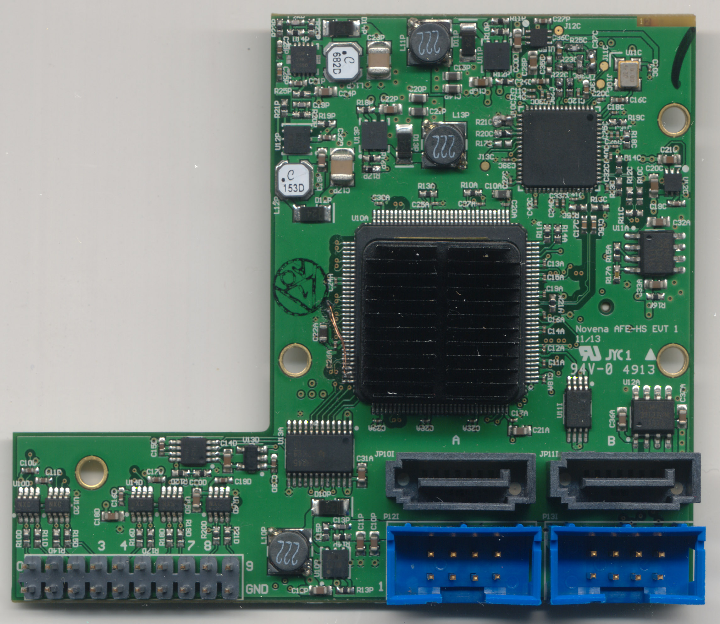
MyriadRF continues to move forward with their SDR solution for Novena. About three weeks ago they sent us pre-production boards, and they are looking good. We’ve placed a binding order for their boards, and things look on track to get them into our shop by November, in time for integration with the first desktop units we’ll be shipping. MyriadRF is working on a fun demo for their hardware, but I’ll save that story for them to tell :)
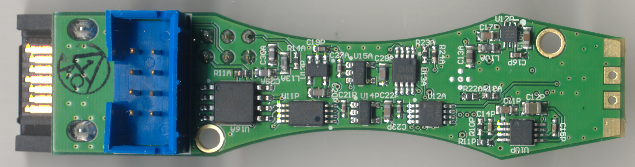
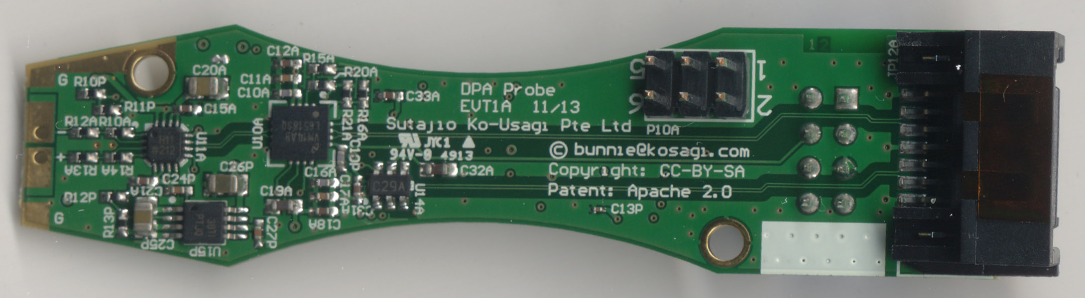
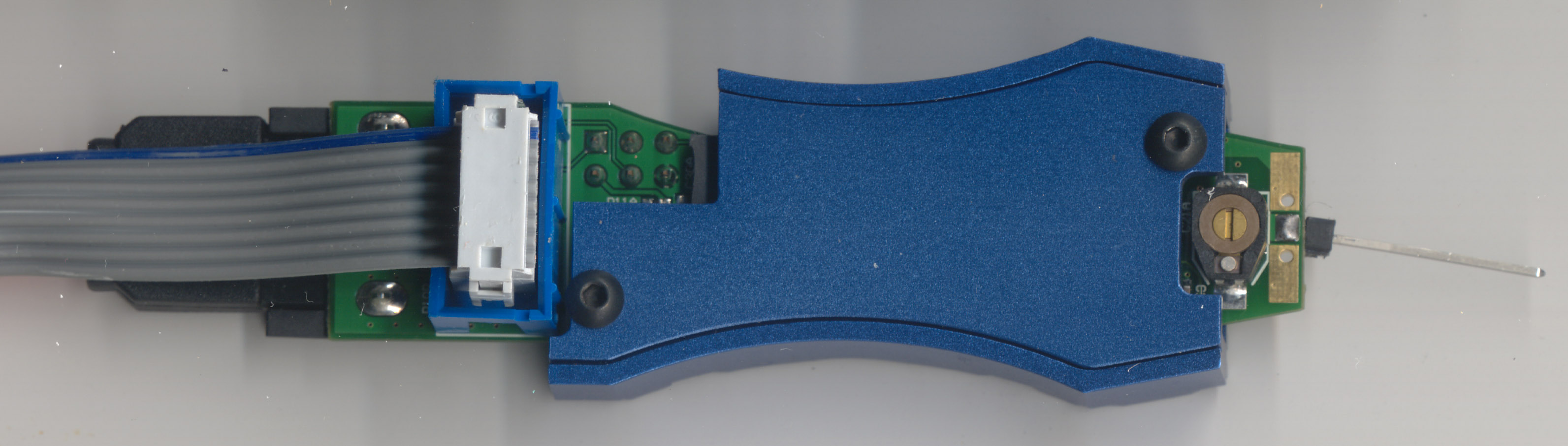
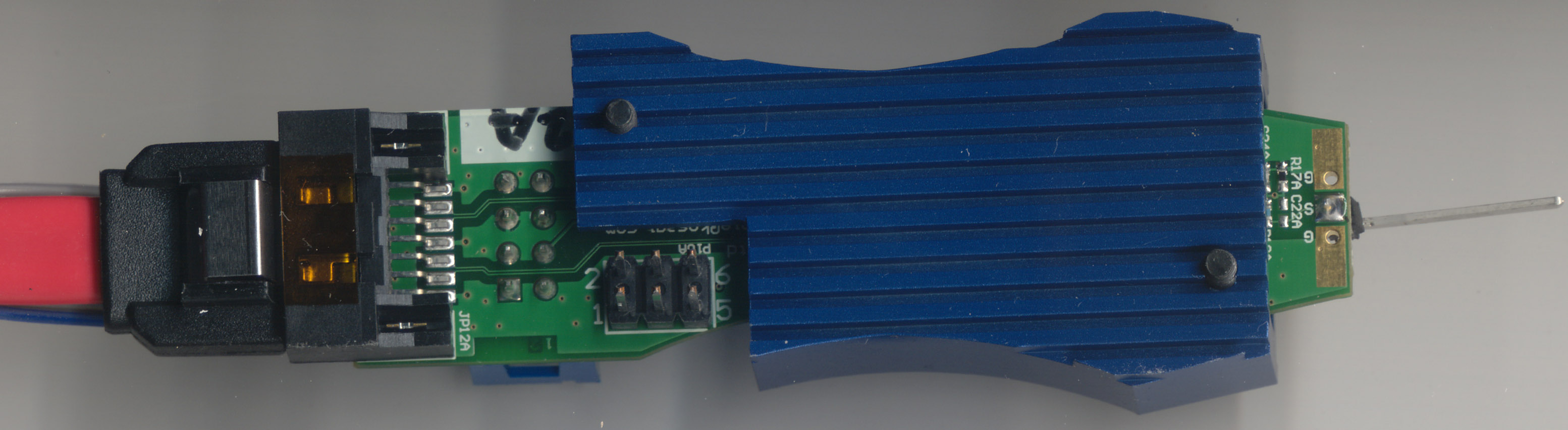
The CrypTech group has also been developing applications with the help of Novena. The CrypTech project is developing a BSD / CC BY-SA 3.0 licensed reference design and prototype examples of a Hardware Security Module. Their hope is to create a widely reviewed, designed-for-crypto device that anyone can compose for their application and easily build with their own trusted supply chain. They are using Novena to prototype elements of their design.
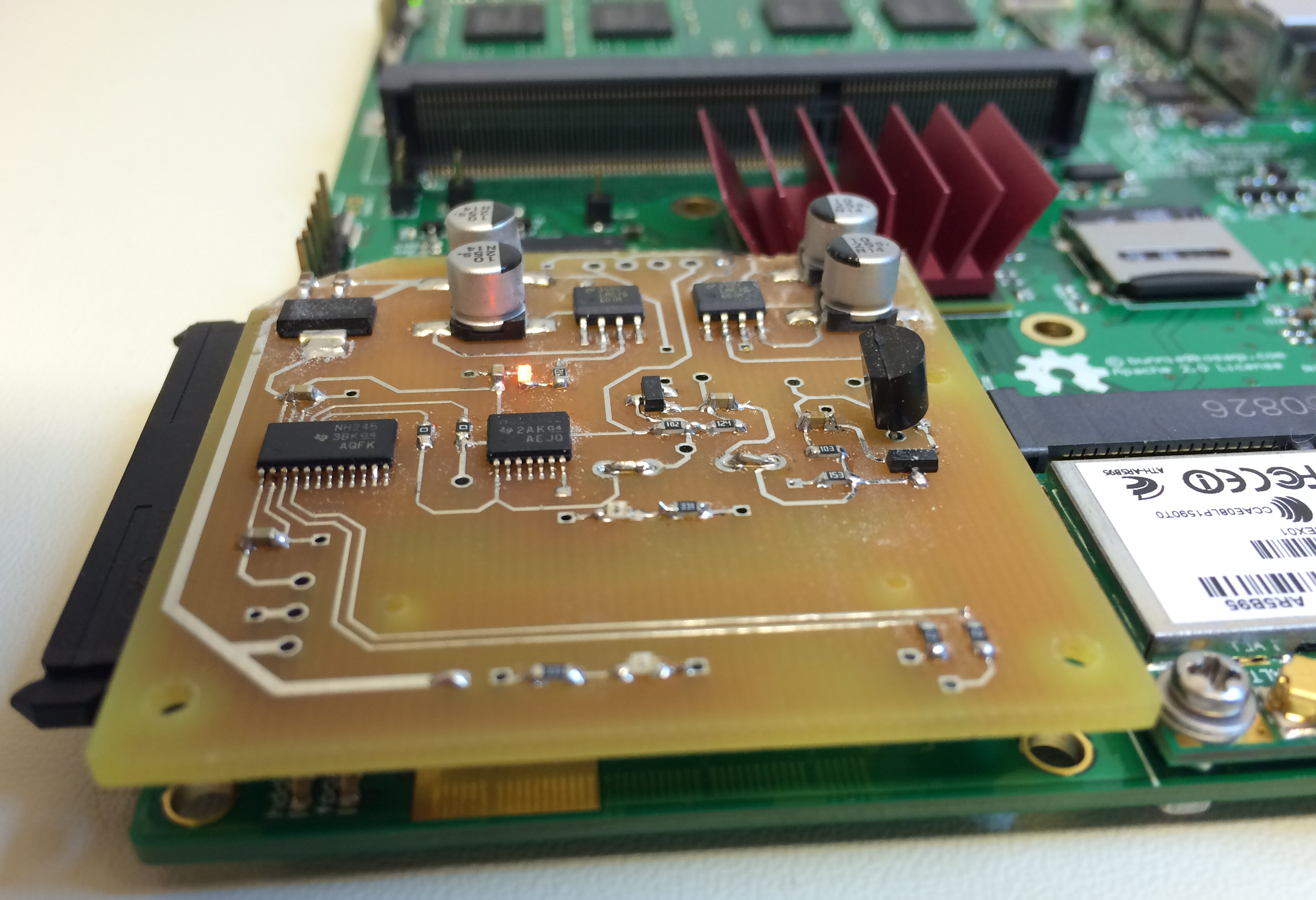
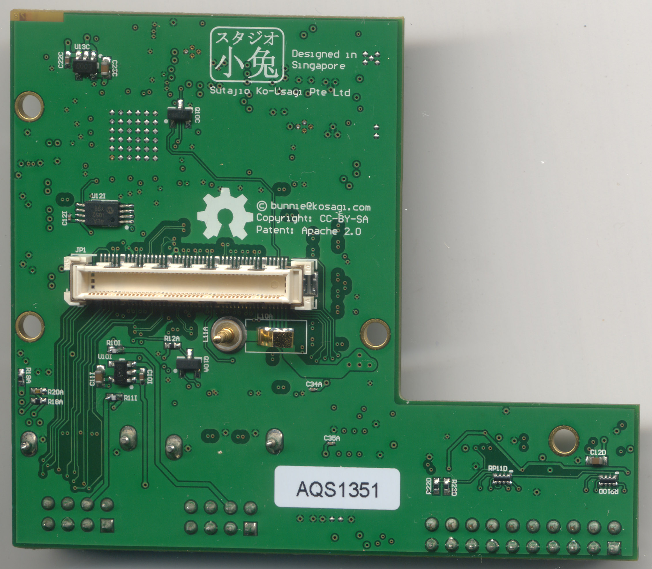
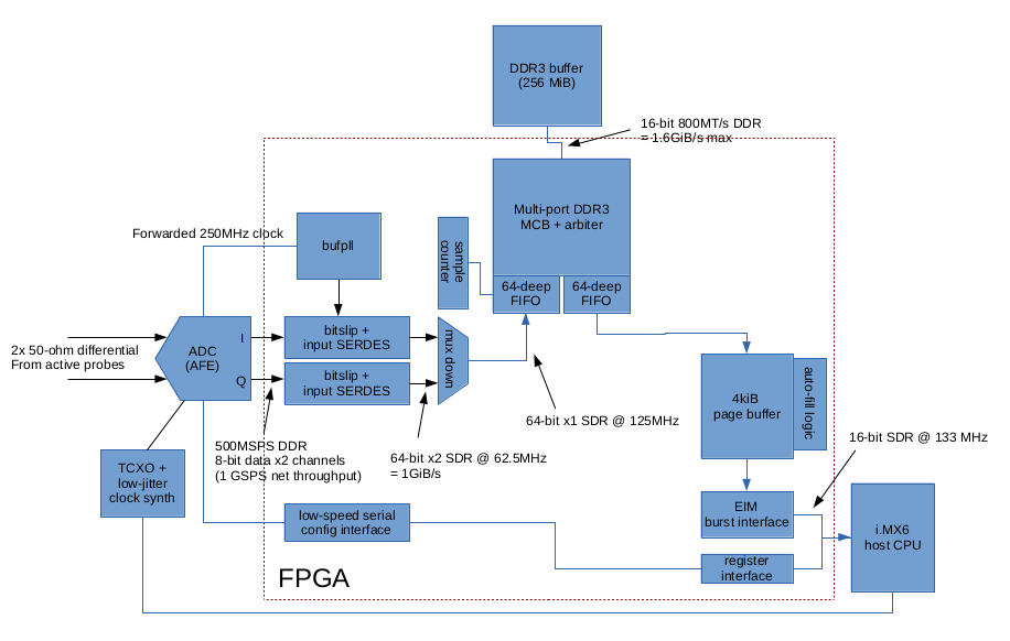
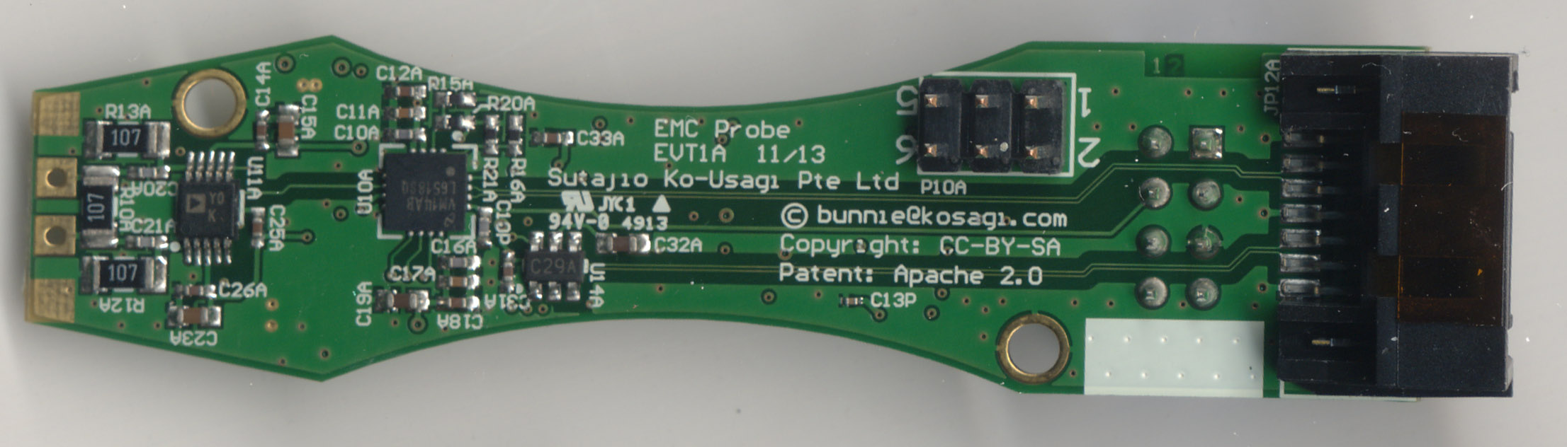
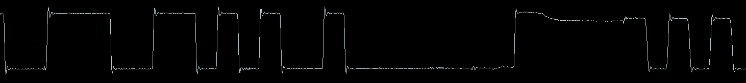
The expansion board highlighted above is a prototype noise source based on avalanche noise from the transistor that can be seen on the middle of the board. CrypTech uses that noise to generate entropy in the FPGA. The entropy is then combined with entropy generated by ring oscillators in the FPGA and mixed using e.g. SHA-512 to generate seeds. The seeds are then used to initialize the ChaCha stream cipher, ultimately resulting in a stream of cryptographically sound random values. The result is a high performance, state-of-the art random number generator coprocessor. This of course represents just a first draft; since the implementation is done in an FPGA, the CrypTech team will continue to evolve their methodology and experiment with alternative methods to generate a robust stream of random numbers.
Thanks to the CrypTech team for sharing a sneak-peek of their baby!
Looking Forward
From our current progress, it seems we’re still largely on track to release an initial shipment of bare boards to early backers in late November, and have an initial shipment of desktop units ready to go by late December. We’ll be shipping the units in tranches, so some backers will receive units before others.
Our shipping algorithm is roughly a combination of how early someone backed the campaign, modified by which region of the world you’re in. As every country has different customs issues, we will probably ship just one or two items to each unique country first to uncover any customs or regulatory problems, before attempting to ship in bulk. This means backers outside the United States (where Crowd Supply’s fulfillment center is located) will be receiving their units a bit later than those within the US.
And as a final note, if there’s one thing we’ve learned in the hardware business, is that you can’t count your chickens before they’ve hatched. Good progress to date doesn’t mean we’ve got an easy path to finished units. We still have a lot of hills to climb and rivers to cross, but at least for now we seem to be on track.
Thanks again to all of our Novena backers, we’re looking forward to getting hardware into your hands soon!
-bunnie & xobs