Archive for the ‘betrusted’ Category

Precursor: From Boot to Root

Wednesday, February 16th, 2022

I have always wanted a computer that was open enough that it can be inspected for security, and also simple enough that I could analyze it in practice. Precursor is a step towards that goal.

As a test, I made a one hour video that walks through the Precursor tech stack, from hardware to root keys. I feel it’s a nice demo of what evidence-based trust should look like:

The video is a bit of a firehose, so please refer to our wiki for more info, or open an issue to further the discussion.

Erratum #1: I had mistakenly attributed SpinalHDL as a subset of Chisel. SpinalHDL is actually a separately developed HDL by Charles Papon. It was developed contemporaneously with Chisel and inspired by many concepts in it, such as using Scala as the underlying language; but it is not affiliated with Chisel.

The Plausibly Deniable DataBase (PDDB)

Tuesday, February 8th, 2022

The problem with building a device that is good at keeping secrets is that it turns users into the weakest link.


From xkcd, CC-BY-NC 2.5

In practice, attackers need not go nearly as far as rubber-hose cryptanalysis to obtain passwords; a simple inspection checkpoint, verbal threat or subpoena is often sufficiently coercive.

Most security schemes facilitate the coercive processes of an attacker because they disclose metadata about the secret data, such as the name and size of encrypted files. This allows specific and enforceable demands to be made: “Give us the passwords for these three encrypted files with names A, B and C, or else…”. In other words, security often focuses on protecting the confidentiality of data, but lacks deniability.

A scheme with deniability would make even the existence of secret files difficult to prove. This makes it difficult for an attacker to formulate a coherent demand: “There’s no evidence of undisclosed data. Should we even bother to make threats?” A lack of evidence makes it more difficult to make specific and enforceable demands.

Thus, assuming the ultimate goal of security is to protect the safety of users as human beings, and not just their files, enhanced security should come hand-in-hand with enhanced plausible deniability (PD). PD arms users with a set of tools they can use to navigate the social landscape of security, by making it difficult to enumerate all the secrets potentially contained within a device, even with deep forensic analysis.

Precursor is a device we designed to keep secrets, such as passwords, wallets, authentication tokens, contacts and text messages. We also want it to offer plausible deniability in the face of an attacker that has unlimited access to a physical device, including its root keys, and a set of “broadly known to exist” passwords, such as the screen unlock password and the update signing password. We further assume that an attacker can take a full, low-level snapshot of the entire contents of the FLASH memory, including memory marked as reserved or erased. Finally, we assume that a device, in the worst case, may be subject to repeated, intrusive inspections of this nature.

We created the PDDB (Plausibly Deniable DataBase) to address this threat scenario. The PDDB aims to offer users a real option to plausibly deny the existence of secret data on a Precursor device. This option is strongest in the case of a single inspection. If a device is expected to withstand repeated inspections by the same attacker, then the user has to make a choice between performance and deniability. A “small” set of secrets (relative to the entire disk size, on Precursor that would be 8MiB out of 100MiB total size) can be deniable without a performance impact, but if larger (e.g. 80MiB out of 100MiB total size) sets of secrets must be kept, then archived data needs to be turned over frequently, to foil ciphertext comparison attacks between disk imaging events.

The API Problem

“Never roll your own crypto”, and “never roll your own filesystem”: two timeless pieces of advice worth heeding. Yet, the PDDB is both a bit of new crypto, and a lot of new filesystem (and I’m not particularly qualified to write either). So, why take on the endeavor, especially when deniability is not a new concept?

For example, one can fill a disk with random data, and then use a Veracrypt hidden volume, or LUKS with detached partition headers. So long as the entire disk is pre-filled with random data, it is difficult for an attacker to prove the existence of a hidden volume with these pre-existing technologies.

Volume-based schemes like these suffer from what I call the “API Problem”. While the volume itself may be deniable, it requires application programs to be PD-aware to avoid accidental disclosures. For example, they must be specifically coded to split user data into multiple secret volumes, and to not throw errors when the secret volumes are taken off-line. This substantially increases the risk of unintentional leakage; for example, an application that is PD-naive could very reasonably throw an error message informing the user (and thus potentially an attacker) of a supposedly non-existent volume that was taken off-line. In other words, having the filesystem itself disappear is not enough; all the user-level applications should be coded in a PD-aware fashion.

On the other hand, application developers are typically not experts in cryptography or security, and they might reasonably expect the OS to handle tricky things like PD. Thus, in order to reduce the burden on application developers, the PDDB is structured not as a traditional filesystem, but as a single database of dictionaries containing many key-value pairs.

Secrets are overlaid or removed from the database transparently, through a mechanism called “Bases” (the plural of a single “Basis”, similar to the concept of a vector basis from linear algebra). The application-facing view of data is computed as the union of the key/value pairs within the currently unlocked secret Bases. In the case that the same key exists within dictionaries with the same name in more than one Basis, by default the most recently unlocked key/value pairs take precedence over the oldest. By offering multiple views of the same dataset based on the currently unlocked set of secrets, application developers don’t have to do anything special to leverage the PD aspects of the PDDB.

The role of a Basis in PD is perhaps best demonstrated through a thought experiment centered around the implementation of a chat application. In Precursor, the oldest (first to be unlocked) Basis is always the “System” Basis, which is unlocked on boot by the user unlock password. Now let’s say the chat application has a “contact book”. Let’s suppose the contact book is implemented as a dictionary called “chat.contacts”, and it exists in the (default) System Basis. Now let’s suppose the user adds two contacts to their contact book, Alice and Bob. The contact information for both will be stored as key/value pairs within the “chat.contacts” dictionary, inside the System Basis.

Now, let’s say the user wants to add a new, secret contact for Trent. The user would first create a new Basis for Trent – let’s say it’s called “Trent’s Basis”. The chat application would store the new contact information in the same old dictionary called “chat.contacts”, but the PDDB writes the contact information to a key/value pair in a second copy of the “chat.contacts” dictionary within “Trent’s Basis”.

Once the chat with Trent is finished, the user can lock Trent’s Basis (it would also be best practice to refresh the chat application). This causes the key/value pair for Trent to disappear from the unionized view of “chat.contacts” – only Alice and Bob’s contacts remain. Significantly, the “chat.contacts” dictionary did not disappear – the application can continue to use the same dictionary, but future queries of the dictionary to generate a listing of available contacts will return only Alice and Bob’s key/value pairs; Trent’s key/value pair will remain hidden until Trent’s Basis is unlocked again.

Of course, nothing prevents a chat application from going out of its way to maintain a separate copy of the contact book, thus allowing it to leak the existence of Trent’s key/value pair after the secret Basis is closed. However, that is extra work on behalf of the application developer. The idea behind the PDDB is to make the lowest-effort method also the safest method. Keeping a local copy of the contacts directory takes effort, versus simply calling the dict_list() API on the PDDB to extract the contact list on the fly. However, the PDDB API also includes a provision for a callback, attached to every key, that can inform applications when a particular key has been subtracted from the current view of data due to a secret Basis being locked.

Contrast this to any implementation using e.g. a separate encrypted volume for PD. Every chat application author would have to include special-case code to check for the presence of the deniable volumes, and to unionize the contact book. Furthermore, the responsibility to not leak un-deniable references to deniable volumes inside the chat applications falls squarely on the shoulders of each and every application developer.

In short, by pushing the deniability problem up the filesystem stack to the application level, one greatly increases the chances of accidental disclosure of deniable data. Thus a key motivation for building the PDDB is to provide a set of abstractions that lower the effort for application developers to take advantage of PD, while reducing the surface of issues to audit for the potential leakage of deniable data.

Down the Rabbit Hole: The PDDB’s Internal Layout

Since we’re taking a clean-sheet look at building an encrypted, plausibly-deniable filesystem, I decided to start by completely abandoning any legacy notion of disks and volumes. In the case of the PDDB, the entire “disk” is memory-mapped into the virtual memory space of the processor, on 4k-page boundaries. Like the operating system Xous, the entire PDDB is coded to port seamlessly between both 32-bit and 64-bit architectures. Thus, on a 32-bit machine, the maximum size of the PDDB is limited to a couple GiB (since it has to share memory space with the OS), but on a 64-bit machine the maximum size is some millions of terabytes. While a couple GiB is small by today’s standards, it is ample for Precursor because our firmware blob-free, directly-managed, high write-lifetime FLASH memory device is only 128MiB in size.

Each Basis in the PDDB has its own private 64-bit memory space, which are multiplexed into physical memory through the page table. It is conceptually similar to the page table used to manage the main memory on the CPU: each physical page of storage maps to a page table entry by shifting its address to the right by 12 bits (the address width of a 4k page). Thus, Precursor’s roughly 100MiB of available FLASH memory maps to about 25,000 entries. These entries are stored sequentially at the beginning of the PDDB physical memory space.

Unlike a standard page table, each entry is 128 bits wide. An entry width of 128 bits allows each page table entry to be decrypted and encrypted independently with AES-256 (recall that even though the key size is 256 bits, the block size remains at 128 bits). 56 bits of the 128 bits in the page table entry are used to encode the corresponding virtual address of the entry, and the rest are used to store flags, a nonce and a checksum. When a Basis is unlocked, each of the 25,000 page table entries are scanned by decrypting them using the unlock key for candidates that have a matching checksum; all the candidates are stored in a hash table in RAM for later reference. We call them “entry candidates” because the checksum is too small to be cryptographically secure; however, the actual page data itself is protected using AES-GCM-SIV, which provides cryptographically strong authentication in addition to confidentiality.

Fortunately, our CPU, like most other modern CPUs, support accelerated AES instructions, so scanning 25k AES blocks for valid pages does not take a long time, just a couple of seconds.

To recap, every time a Basis is unlocked, the page table is scanned for entries that decrypt correctly. Thus, each Basis has its own private 64-bit memory space, multiplexed into physical memory via the page table, allowing us to have multiple, concurrent cryptographic Bases.

Since every Basis is orthogonal, every Basis can have the exact same virtual memory layout, as shown below. The layout always uses 64-bit addressing, even on 32-bit machines.

|   Start Address        |                                           |
|------------------------|-------------------------------------------|
| 0x0000_0000_0000_0000  |  Invalid -- VPAGE 0 reserved for Option   |
| 0x0000_0000_0000_0FE0  |  Basis root page                          |
| 0x0000_0000_00FE_0000  |  Dictionary[0]                            |
|                    +0  |    - Dict header (127 bytes)              |
|                   +7F  |    - Maybe key entry (127 bytes)          |
|                   +FE  |    - Maybe key entry (127 bytes)          |
|              +FD_FF02  |    - Last key entry start (128k possible) |
| 0x0000_0000_01FC_0000  |  Dictionary[1]                            |
| 0x0000_003F_7F02_0000  |  Dictionary[16382]                        |
| 0x0000_003F_8000_0000  |  Small data pool start  (~256GiB)         |
|                        |    - Dict[0] pool = 16MiB (4k vpages)     |
|                        |      - SmallPool[0]                       |
|                  +FE0  |      - SmallPool[1]
| 0x0000_003F_80FE_0000  |    - Dict[1] pool = 16MiB                 |
| 0x0000_007E_FE04_0000  |    - Dict[16383] pool                     |
| 0x0000_007E_FF02_0000  |  Unused                                   |
| 0x0000_007F_0000_0000  |  Medium data pool start                   |
|                        |    - TBD                                  |
| 0x0000_FE00_0000_0000  |  Large data pool start  (~16mm TiB)       |
|                        |    - Demand-allocated, bump-pointer       |
|                        |      currently no defrag                  |

The zeroth page is invalid, so we can have “zero-cost” Option abstractions in Rust by using the NonZeroU64 type for Basis virtual addresses. Also note that the size of a virtual page is 0xFE0 (4064) bytes; 32 bytes of overhead on each 4096-byte physical page are consumed by a journal number plus AES-GCM-SIV’s nonce and MAC.

The first page contains the Basis Root Page, which contains the name of the Basis as well as the number of dictionaries contained within the Basis. A Basis can address up to 16,384 dictionaries, and each dictionary can address up to 131,071 keys, for a total of up to 2 billion keys. Each of these keys can map a contiguous blob of data that is limited to 32GiB in size.

The key size cap can be adjusted to a larger size by tweaking a constant in the API file, but it is a trade-off between adequate storage capacity and simplicity of implementation. 32GiB is not big enough for “web-scale” applications, but it’s large enough to hold a typical Blu-Ray movie as a single key, and certainly larger than anything that Precursor can handle in practice with its 32-bit architecture. Then again, nothing about Precursor, or its intended use cases, are web-scale. The advantage of capping key sizes at 32GiB is that we can use a simple “bump allocator” for large data: every new key reserves a fresh block of data in virtual memory space that is 32GiB in size, and deleted keys simply “leak” their discarded space. This means that the PDDB can handle a lifetime total of 200 million unique key allocations before it exhausts the bump allocator’s memory space. Given that the write-cycle lifetime of the FLASH memory itself is only 100k cycles per sector, it’s more likely that the hardware will wear out before we run out of key allocation space.

To further take pressure off the bump allocator, keys that are smaller than one page (4kiB) are merged together and stored in a dedicated “small key” pool. Each dictionary gets a private pool of up to 16MiB storage for small keys before they fall back to the “large key” pool and allocate a 32GiB chunk of space. This allows for the efficient storage of small records, such as system configuration data which can consist of hundreds of keys, each containing just a few dozen bytes of data. The “small key” pool has an allocator that will re-use pages as they become free, so there is no lifetime limit on unique allocations. Thus the 200-million unique key lifetime allocation limit only applies to keys that are larger than 4kiB. We refer readers to YiFang Wang’s master thesis for an in-depth discussion of the statistics of file size, usage and count.

Keeping Secret Bases Secret

As mentioned previously, most security protocols do a good job of protecting confidentiality, but do little to hide metadata. For example, user-based password authentication protocols can do a good job of keeping the password a secret, but the existence of a user is plain to see, since the username, salt, and password hash are recorded in an unencrypted database. Thus, most standard authentication schemes that rely on unique salts would also directly disclose the existence of secret Bases through a side channel consisting of Basis authentication metadata.

Thus, we use a slightly modified key derivation function for secret Bases. The PDDB starts with a per-device unique block of salt that is fixed and common to all Bases on that device. This salt is hashed with the user-provided name of the Basis to generate a per-Basis unique salt, which is then combined with the password using bcrypt to generate a 24-byte password hash. This password is then expanded to 32 bytes using SHA512/256 to generate the final AES-256 key that is used to unlock a Basis.

This scheme has the following important properties:

  • No metadata to leak about the presence of secret Bases
  • A unique salt per device
  • A unique (but predictable given the per-device salt and Basis name) salt per-Basis
  • No storage of the password or metadata on-device
  • No compromise in the case that the root keys are disclosed
  • No compromise of other secret Bases if passwords are disclosed for some of the Bases

This scheme does not offer forward secrecy in and of itself, in part because this would increase the wear-load of the FLASH memory and substantially degrade filesystem performance.

Managing Free Space

The amount of free space available on a device is a potent side channel that can disclose the existence of secret data. If a filesystem always faithfully reports the amount of free space available, an attacker can deduce the existence of secret data by simply subtracting the space used by the data decrypted using the disclosed passwords from the total space of the disk, and compare it to the reported free space. If there is less free space reported, one may conclude that additional hidden data exists.

As a result PD is a double-edged sword. Locked, secret Bases must walk and talk exactly like free space. I believe that any effective PD system is fundamentally vulnerable to a loss-of-data attack where an attacker forces the user to download a very large file, filling all the putative “free space” with garbage, resulting in the erasure of any secret Bases. Unfortunately, the best work-around I have for this is to keep backups of your archival data on another Precursor device that is kept in a secure location.

That being said, the requirement for no sidechannel through free space is at direct odds with performance and usability. In the extreme, any time a user wishes to allocate data, they must unlock all the secret Bases so that the true extent of free space can be known, and then the secret Bases are re-locked after the allocation is completed. This scheme would leak no information about the amount of data stored on the device when the Bases are locked.

Of course, this is a bad user experience and utterly unusable. The other extreme is to keep an exact list of the actual free space on the device, which would protect any secret data without having to ever unlock the secrets themselves, but would provide a clear measure of the total amount of secret data on the device.

The PDDB adopts a middle-of-the-road solution, where a small subset of the true free space available on disk is disclosed, and the rest is maybe data, or maybe free space. We call this deliberately disclosed subset of free space the “FastSpace cache”. To be effective, the FastSpace cache is always a much smaller number than the total size of the disk. In the case of Precursor, the total size of the PDDB is 100MiB, and the FastSpace cache records the location of up to 8MiB of free pages.

Thus, if an attacker examines the FastSpace cache and it contains 1MiB of free space, it does not necessarily mean that 99MiB of data must be stored on the device; it could also be that the user has written only 7MiB of data to the device, and in fact the other 93MiB are truly free space, or any number of other scenarios in between.

Of course, whenever the FastSpace cache is exhausted, the user must go through a ritual of unlocking all their secret Bases, otherwise they run the risk of losing data. For a device like Precursor, this shouldn’t happen too frequently because it’s somewhat deliberately not capable of handling rich media types such as photos and videos. We envision Precursor to be used mainly for storing passwords, authentication tokens, wallets, text chat logs and the like. It would take quite a while to fill up the 8MiB FastSpace cache with this type of data. However, if the PDDB were ported to a PC and scaled up to the size of, for example, an entire 500GiB SSD, the FastSpace cache could likewise be grown to dozens of GiB, allowing a user to accumulate a reasonable amount of rich media before having to unlock all Bases and renew their FastSpace cache.

This all works fairly well in the scenario that a Precursor must survive a single point inspection with full PD of secret Bases. In the worst case, the secrets could be deleted by an attacker who fills the free space with random data, but in no case could the attacker prove that secret data existed from forensic examination of the device alone.

This scheme starts to break down in the case that a user may be subject to multiple, repeat examinations that involve a full forensic snapshot of the disk. In this case, the attacker can develop a “diff” profile of sectors that have not changed between each inspection, and compare them against the locations of the disclosed Bases. The remedy to this would be a periodic “scrub” where entries have their AES-GCM-SIV nonce renewed. This actually happens automatically if a record is updated, but for truly read-only archive data its location and nonce would remain fixed on the disk over time. The scrub procedure has not yet been implemented in the current release of the PDDB, but it is a pending feature. The scrub could be fast if the amount of data stored is small, but a re-noncing of the entire disk (including flushing true free space with new tranches of random noise) would be the most robust strategy in the face of an attacker that is known to take repeated forensic snapshots of a user’s device.

Code Location and Wrap-Up

If you want to learn more about the details of the PDDB, I’ve embedded extensive documentation in the source code directly. The API is roughly modeled after Rust’s std::io::File model, where a .get() call is similar to the usual .open() call, and then a handle is returned which uses Read and Write traits for interaction with the key data itself. For a “live” example of its usage, users can have a look at WiFi connection manager, which saves a list of access points and their WPA keys in a dictionary: code for saving an entry, code for accessing entries.

Our CI tests contain examples of more interesting edge cases. We also have the ability to save out a PDDB image in “hosted mode” (that is, with Xous directly running on your local machine) and scrub through its entrails with a Python script that greatly aids with debugging edge cases. The debugging script is only capable of dumping and analyzing a static image of the PDDB, and is coded to “just work well enough” for that job, but is nonetheless a useful resource if you’re looking to go deeper into the rabbit hole.

Please keep in mind that the PDDB is very much in its infancy, so there are likely to be bugs and API-breaking changes down the road. There’s also a lot of work that needs to be done on the UX for the PDDB. At the moment, we only have Rust API calls, so that applications can create and use secret Bases as well as dictionaries and keys. There currently are no user-facing command line tools, or a graphical “File Explorer” style tool available, but we hope to remedy this soon. However, I’m very happy that we were able to complete the core implementation of the PDDB. I’m hopeful that out-of-the-box, application developers for Precursor will start using the PDDB for data storage, so that we can start a community dialogue on the overall design.

This work was funded in part through the NGI0 PET Fund, a fund established by NLNet with financial support from the European Commission’s Next Generation Internet Programme.

Fixing a Tiny Corner of the Supply Chain

Tuesday, December 14th, 2021

No product gets built without at least one good supply chain war story – especially true in these strange times. Before we get into the details of the story, I feel it’s worth understanding a bit more about the part that caused me so much trouble: what it does, and why it’s so special.

The Part that Could Not Be Found
There’s a bit of magic in virtually every piece of modern electronics involved in the generation of internal timing signals. It’s called an oscillator, and typically it’s implemented with a precisely cut fleck of quartz crystal that “rings” when stimulated, vibrating millions of times per second. The accuracy of the crystal is measured in parts-per-million, such that over a month – about 2.5 million seconds – a run-of-the-mill crystal with 50ppm accuracy might drift by about two minutes. In mechanical terms it’s like producing 1kg (2.2 pound) bags of rice that have precisely no more and no less than one grain of rice compared to each other; or in CS terms it’s about 15 bits of precision (it’s funny how one metric sounds hard, while the other sounds trivial).

One of the many problems with quartz crystals is that they are big. Here’s a photo from wikipedia of the inside of a typical oscillator:


CC BY-SA 4.0 by Binarysequence via Wikipedia

The disk on the left is the crystal itself. Because the frequency of the crystal is directly related to its size, there’s a “physics limit” on how small these things can be. Their large size also imposes a limit on how much power it takes to drive them (it’s a lot). As a result, they tend to be large, and power-hungry – it’s not uncommon for a crystal oscillator to be specified to consume a couple milliamperes of current in normal operation (and yes, there are also chips with built-in oscillator circuits that can drive crystals, which reduces power; but they, too, have to burn the energy to charge and discharge some picofarads of capacitance millions of times per second due to the macroscopic nature of the crystal itself).

A company called SiTime has been quietly disrupting the crystal industry by building MEMS-based silicon resonators that can outperform quartz crystals in almost every way. The part I’m using is the SiT8021, and it’s tiny (1.5×0.8mm), surface-mountable (CSBGA), consumes about 100x less power than the quartz-based competition, and has a comparable frequency stability of 100ppm. Remarkably, despite being better in almost every way, it’s also cheaper – if you can get your hands on it. More on that later.

Whenever something like this comes along, I always like to ask “how come this didn’t happen sooner?”. You usually learn something interesting in exploring that question. In the case of pure-silicon oscillators, they have been around forever, but they are extremely sensitive to temperature and aging. Anyone who has designed analog circuits in silicon are familiar with the problem that basically every circuit element is a “temperature-to-X” converter, where X is the parameter you wish you could control. For example, a run of the mill “ring oscillator” with no special compensation would have an initial frequency accuracy of about 50% – going back to our analogies, it’d be like getting a bag of rice that nominally holds 1kg, but is filled to an actual weight of somewhere between 0.5kg and 1.5kg – and you would get swings of an additional 30% depending upon the ambient temperature. A silicon MEMS oscillator is a bit better than that, but its frequency output would still vary wildly with temperature; orders of magnitude more than the parts-per-million specified for a quartz crystal.

So, how do they turn something so innately terrible into something better-than-quartz? First I took a look at the devices under a microscope, and it’s immediately obvious that it’s actually two chips that have been bonded face-to-face with each other.


Edge-on view of an SiT8021 already mounted on a circuit board.

I deduced that a MEMS oscillator chip is nestled between the balls that bond the chip to the PCB. I did a quick trawl through the patents filed by SiTimes, and I’m guessing the MEMS oscillator chip contains at least two separate oscillators. These oscillators are intentionally different, so that their frequency drift with temperature also have different, but predictable, curves. They can use the relative difference of the frequencies to very precisely measure the absolute temperature of the pair of oscillators by comparing the instantaneous difference between the two frequencies. In other words, they took the exact problem that plagues silicon designs, and turned it into a feature: they built a very precise temperature sensor out of two silicon oscillators.

With the temperature of the oscillators known to exquisite precision, one can now compensate for the temperature effects. That’s what the larger of the two chips (the one directly attached to the solder balls) presumably does. It computes an inverse mapping of temperature vs. frequency, constantly adjusting a PLL driven by one of the two MEMs oscillators, to derive a precise, temperature-stable net frequency. The controller chip presumably also contains a set of eFuses that are burned in the factory (or by the distributor) to calibrate and set the initial frequency of the device. I didn’t do an acid decap of the controller chip, but it’s probably not unreasonable for it to be fabricated in 28nm silicon; at this geometry you could fit an entire RISC-V CPU in there with substantial microcode and effectively “wrap a computer” around the temperature drift problem that plagues silicon designs.

Significantly, the small size of the MEMS resonator compared to a quartz crystal, along with its extremely intimate bonding to the control electronics, means a fundamentally lower limit on the amount of energy required to sustain resonance, which probably goes a long way towards explaining why this circuit is able to reduce active power by so much.

The tiny size of the controller chip means that a typical 300mm wafer will yield about 50,000 chips; going by the “rule of thumb” that a processed wafer is roughly $3k, that puts the price of a raw, untested controller chip at about $0.06. The MEMs device is presumably a bit more expensive, and the bonding process itself can’t be cheap, but at a “street price” of about $0.64 each in 10k quantities, I imagine SiTime is still making good margin. All that being said, a million of these oscillators would fit on about 18 wafers, and the standard “bulk” wafer cassette in a fab holds 25 wafers (and a single fab will pump out about 25,000 – 50,000 wafers a month); so, this is a device that’s clearly ready for mobile-phone scale production.

Despite the production capacity, the unique characteristics of the SiT8021 make it a strong candidate to be designed into mobile phones of all types, so I would likely be competing with companies like Apple and Samsung for my tiny slice of the supply chain.

The Supply Chain War Story
It’s clearly a great part for a low-power mobile device like Precursor, which is why I designed it into the device. Unfortunately, there’s also no real substitute for it. Nobody else makes a MEMS oscillator of comparable quality, and as outlined above, this device is smaller and orders of magnitude lower power than an equivalent quartz crystal. It’s so power-efficient that in many chips it is less power to use this off-chip oscillator, than to use the built-in crystal oscillator to drive a passive crystal. For example, the STM32H7 HSE burns 450uA, whereas the SiT8021 runs at 160uA. To be fair, one also has to drive the pad input capacitance of the STM32, but even with that considered you’re probably around 250uA.

To put it in customer-facing terms, if I were forced to substitute commonly available quartz oscillators for this part, the instant-on standby time of a Precursor device would be cut from a bit over 50 hours down to about 40 hours (standby current would go from 11mA up to 13mA).

If this doesn’t make the part special enough, the fact that it’s an oscillator puts it in a special class with respect to electromagnetic compliance (EMC) regulations. These are the regulations that make sure that radios don’t interfere with each other, and like them or not, countries take them very seriously as trade barriers – by requiring expensive certifications, you’re able to eliminate the competition of small upstarts and cheap import equipment on “radio safety” grounds. Because the quality of radio signals depend directly upon the quality of the oscillator used to derive them, the regulations (quite reasonably) disallow substitutions of oscillators without re-certification. Thus, even if I wanted to take the hit on standby time and substitute the part, I’d have to go through the entire certification process again, at a cost of several thousand dollars and some weeks of additional delay.

Thus this part, along with the FPGA, is probably one of the two parts on the entire BOM that I really could not do without. Of course, I focused a lot on securing the FPGA, because of its high cost and known difficulty to source; but for want of a $0.68 crystal, a $565 product would not be shipped…

The supply chain saga starts when I ordered a couple thousand of these in January 2021, back when it had about a 30 week lead time, giving a delivery sometime in late August 2021. After waiting about 28 weeks, on August 12th, we got an email from our distributor informing us that they had to cancel our entire order for SiT8021s. That’s 28 weeks lost!

The nominal reason given was that the machine used to set the frequency of the chips was broken or otherwise unavailable, and due to supply chain problems it couldn’t be fixed anytime soon. Thus, we had to go to the factory to get the parts. But, in order to order direct from the factory, we had to order 18,000 pieces minimum – over 9x of what I needed. Recall that one wafer yields 58,000 chips, so this isn’t even half a wafer’s worth of oscillators. That being said, 18,000 chips would be about $12,000. This isn’t chump change for a project operating on a fixed budget. It’s expensive enough that I considered recertification of the product to use a different oscillator, if it weren’t for the degradation in standby time.

Panic ensues. We immediately trawl all the white-market distributor channels and buy out all the stock, regardless of the price. Instead of paying our quoted rate of $0.68, we’re paying as much as $1.05 each, but we’re still short about 300 oscillators.

I instruct the buyers to search the gray market channels, and they come back with offers at $5 or $6 for the $0.68 part, with no guarantee of fitness or function. In other words, I could pay 10x of the value of the part and get a box of bricks, and the broker could just disappear into the night with my money.

No deal. I had to do better.

By this time, every distributor was repeating the “18k Minimum Order Quantity (MOQ) with long lead time” offer, and my buyers in China waved the white flag and asked me to intervene. After trawling the Internet for a couple hours, I discover that Element14 right here in Singapore (where I live) claims to be able to deliver small quantities of the oscillator before the end of the year. It seems too good to be true.

I ask my buyers in China to place an order, and they balk; the China office repeats that there is simply no stock. This has happened before, due to trade restrictions and regional differences the inventory in one region may not be orderable in another, so I agree to order the balance of the oscillators with a personal credit card, and consign them directly to the factory. At this point, Element14 is claiming a delivery of 10-12 weeks on the Singapore website: that would just meet the deadline for the start of SMT production at the end of November.

I try to convince myself that I had found the solution to the problem, but something smelled rotten. A month later, I check back into the Element14 website to see the status of the order. The delivery had shifted back almost day-for-day to December. I start to suspect maybe they don’t even carry this part, and it’s just an automated listing to honeypot orders into their system. So, I get on the phone with an Element14 representative, and crazy enough, she can’t even find my order in her system even though I can see the order in my own Element14 account. She tells me this is not uncommon, and if she can’t see it in her system, then the web order will never be filled. I’m like, is there any way you can cancel the order then? She’s like “no, because I can’t see the order, I can’t cancel it.” But also because the representative can’t see the order, it also doesn’t exist, and it will never be filled. She recommends I place the order again.

I’m like…what the living fuck. Now I’m starting to sweat bullets; we’re within a few weeks of production start, and I’m considering ordering 18,000 oscillators and reselling the excess as singles via Crowd Supply in a Hail Mary to recover the costs. The frustrating part is, the cost of 300 parts is small – under $200 – but the lack of these parts blocks the shipment of roughly $170,000 worth of orders. So, I place a couple bets across the board. I go to Newark (Element14, but for the USA) and place an order for 500 units (they also claimed to be able to deliver), and I re-placed the order with Element14 Singapore, but this time I put a Raspberry Pi into the cart with the oscillators, as a “trial balloon” to test if the order was actually in their system. They were able to ship the part of the order with the Raspberry Pi to me almost immediately, so I knew they couldn’t claim to “lose the order” like before – but the SiT8021 parts went from having a definitive delivery date to a “contact us for more information” note – not very useful.

I also noticed that by this time (this is mid-October), Digikey is listing most of the SiT8021 parts for immediately delivery, with the exception of the 12MHz, 1.8V version that I need. Now I’m really starting to sweat – one of the hypothesis pushed back at my by the buyer in China was that there was no demand for this part, so it’s been canceled and that’s why I can’t find it anywhere. If the part’s been canceled, I’m really screwed.

I decide it’s time to reach out to SiTime directly. Through hook and crook, I get in touch with a sales rep, who confirms with me that the 12MHz, 1.8V version is a valid and orderable part number, and I should be able to go to Digikey to purchase it. I inform the sales rep that the Digikey website doesn’t list this part number, to which they reply “that’s strange, we’ll look into it”.

Not content to leave it there, I reach out to Digikey directly. I get connected to one of their technical sales representatives via an on-line chat, and after a bit of conversing, I confirmed that in fact the parts are shipped to Digikey as blanks, and they have a machine that can program the parts on-site. The technical sales rep also confirms the machine can program that exact configuration of the part, but because the part is not listed on the website I have to do a “custom part” quotation.

Aha! Now we are getting somewhere. I reach out to their custom-orders department and request a quotation. A lady responds to me fairly quickly and says she’ll get back to me. About a week passes, no response. I ping the department again, no response.

“Uh-oh.”

I finally do the “unthinkable” in the web age – I pick up the phone, and dial in hoping to reach a real human being to plead my case. I dial the extension for the custom department sales rep. It drops straight to voice mail. I call back again, this time punching the number to draw a lottery ticket for a new sales rep.

Luckily, I hit the jackpot! I got connected with a wonderful lady by the name of Mel who heard out my problem, and immediately took ownership for solving the problem. I could hear her typing queries into her terminal, and hemming and hawing over how strange it is for there to be no order code, but she can still pull up pricing. While I couldn’t look over her shoulder, I could piece together that the issue was a mis-configuration in their internal database. After about 5 minutes of tapping and poking, she informs me that she’ll send a message to their web department and correct the issue. Three days later, my part (along with 3 other missing SKUs) is orderable on Digikey, and a week later I have the 300 missing oscillators delivered directly to the factory – just in time for the start of SMT production.

I wrote Mel a hand-written thank-you card and mailed it to Digikey. I hope she received it, because people like here are a rare breed: she has the experience to quickly figure out how the system breaks, the judgment to send the right instructions to the right groups on how to fix it, and the authority to actually make it happen. And she’s actually still working a customer-facing job, not promoted into a corner office management position where she would never be exposed to a real-world problem like mine.

So, while Mel saved my production run, the comedy of errors still plays on at Element14 and Newark. The “unfindable order” is still lodged in my Element14 account, probably to stay there until the end of time. Newark’s “international” department sent me a note saying there’s been an export compliance issue with the part (since when did jellybean oscillators become subject to ITAR restrictions?!), so I responded to their department to give them more details – but got no response back. I’ve since tried to cancel the order, got no response, and now it just shows a status of “red exclamation mark” on hold and a ship date of Jan 2022. The other Singapore Element14 order that was combined with the Raspberry Pi still shows the ominous “please contact us for delivery” on the ship date, and despite trying to contact them, nobody has responded to inquiries. But hey, Digikey’s Mel has got my back, and production is up and (mostly) running on schedule.

This is just is one of many supply chain war stories I’ve had with this production run, but it is perhaps the one with the most unexpected outcome. I feared that perhaps the issue was intense competition for the parts making them unavailable, but the ground truth turned out to be much more mundane: a misconfigured website. Fortunately, this small corner of the supply chain is now fixed, and now anyone can buy the part that caused me so many sleepless nights.

Building a Curve25519 Hardware Accelerator

Thursday, July 15th, 2021

Note: this post uses a $\LaTeX$ plugin to render math symbols. It may require a desktop browser for the full experience…

The “double ratchet” algorithm is integral to modern end-to-end-encrypted chat apps, such as Signal, WhatsApp, and Matrix. It gives encrypted conversations the properties of resilience, forward secrecy, and break-in recovery; basically, even if an adversary can manipulate or observe portions of an exchange, including certain secret materials, the damage is limited with each turn of the double ratchet.

The double-ratchet algorithm is a soup of cryptographic components, but one of the most computationally expensive portions is the “Diffie-Hellman (DH) key exchange”, using Elliptic Curve Diffie-Hellman (ECDH) with Curve25519. How expensive? This post from 2020 claims a speed record of 3.2 million cycles on a Cortex-M0 for just one of the core mathematical operations: fairly hefty. A benchmark of the x25519-dalek Rust crate on a 100 MHz RV32-IMAC implementation clocks in at 100ms per DH key exchange, of which several are involved in a double-ratchet. Thus, any chat client implementation on a small embedded CPU would suffer from significant UI lag.

There are a few strategies to rectify this, ranging from adding a second CPU core to off-load the crypto, to making a full-custom hardware accelerator. Adding a second RISC-V CPU core is expedient, but it wouldn’t do much to force me to understand what I was doing as far as the crypto goes; and there’s already a strong contingent of folks working on multi-core RISC-V on FPGA implementations. The last time I implemented a crypto algorithm was for RSA on a low-end STM32 back in the mid 2000’s. I really enjoyed getting into the guts of the algorithm and stretching my understanding of the underlying mathematical primitives. So, I decided to indulge my urge to tinker, and make a custom hardware accelerator for Curve25519 using Litex/Migen and Rust bindings.

What the Heck Is $\mathbf{{F}}_{{{{2^{{255}}}}-19}}$?

I wanted the accelerator primitive to plug directly into the Rust Dalek Cryptography crates, so that I would be as light-fingered as possible with respect to changes that could lead to fatal flaws in the broader cryptosystem. I built some simple benchmarks and profiled where the most time was being spent doing a double-ratchet using the Dalek Crypto crates, and the vast majority of the time for a DH key exchange was burned in the Montgomery Multiply operation. I won’t pretend to understand all the fancy math-terms, but people smarter than me call it a “scalar multiply”, and it actually consists of thousands of “regular” multiplies on 255-bit numbers, with modular reductions in the prime field $\mathbf{{F}}_{{{{2^{{255}}}}-19}}$, among other things.

Wait, what? So many articles and journals I read on the topic just talk about prime fields, modular reduction and blah blah blah like it’s asking someone to buy milk and eggs at the grocery store. It was a real struggle to try and make sense of all the tricks used to do a modular multiply, much less to say even elliptic curve point transformations.

Well, that’s the point of trying to implement it myself — by building an engine, maybe you won’t understand all the hydrodynamic nuances around fuel injection, but you’ll at least gain an appreciation for what a fuel injector is. Likewise, I can’t say I deeply understand the number theory, but from what I can tell multiplication in $\mathbf{{F}}_{{{{2^{{255}}}}-19}}$ is basically the same as a “regular 255-bit multiply” except you do a modulo (you know, the `%` operator) against the number $2^{{255}}-19$ when you’re done. There’s a dense paper by Daniel J. Bernstein, the inventor of Curve25519, which I tried to read several times. One fact I gleaned is part of the brilliance of Curve25519 is that arithmetic modulo $2^{{255}}-19$ is quite close to regular binary arithmetic except you just need to special-case 19 outcomes out of $2^{{255}}$. Also, I learned that the prime modulus, $2^{{255}}-19$, is where the “25519” comes from in the name of the algorithm (I know, I know, I’m slow!).

After a whole lot more research I stumbled on a paper by Furkan Turan and Ingrid Verbauwhede that broke down the algorithm into terms I could better understand. Attempts to reach out to them to get a copy of the source code was, of course, fruitless. It’s a weird thing about academics — they like to write papers and “share ideas”, but it’s very hard to get source code from them. I guess that’s yet another reason why I never made it in academia — I hate writing papers, but I like sharing source code. Anyways, the key insight from their paper is that you can break a 255-bit multiply down into operations on smaller, 17-bit units called “limbs” — get it? digits are your fingers, limbs (like your arms) hold multiple digits. These 17-bit limbs map neatly into 15 Xilinx 7-Series DSP48E block (which has a fast 27×18-bit multiplier): 17 * 15 = 255. Using this trick we can decompose multiplication in $\mathbf{{F}}_{{{{2^{{255}}}}-19}}$ into the following steps:

  1. Schoolbook multiplication with 17-bit “limbs”
  2. Collapse partial sums
  3. Propagate carries
  4. Is the sum $\geq$ $2^{{255}}-19$?
  5. If yes, add 19; else add 0
  6. Propagate carries again, in case the addition by 19 causes overflows

The multiplier would run about 30% faster if step (6) were skipped. This step happens in a fairly small minority of cases, maybe a fraction of 1%, and the worst-case carry propagate through every 17-bit limb is diminishingly rare. The test for whether or not to propagate carries is fairly straightforward. However, short-circuiting the carry propagate step based upon the properties of the data creates a timing side-channel. Therefore, we prefer a slower but safer implementation, even if we are spending a bunch of cycles propagating zeros most of the time.

Buckle up, because I’m about to go through each step in the algorithm in a lot of detail. One motivation of the exercise was to try to understand the math a bit better, after all!

TL;DR: Magic Numbers

If you’re skimming this article, you’ll see the numbers “19” and “17” come up over and over again. Here’s a quick TL;DR:

  • 19 is the tiny amount subtracted from $2^{{255}}$ to arrive at a prime number which is the largest number allowed in Curve25519. Overflowing this number causes things to wrap back to 0. Powers of 2 map efficiently onto binary hardware, and thus this representation is quite nice for hardware people like me.
  • 17 is a number of bits that conveniently divides 255, and fits into a single DSP hardware primitive (DSP48E) that is available on the target device (Xilinx 7-series FPGA) that we’re using in this post. Thus the name of the game is to split up this 255-bit number into 17-bit chunks (called “limbs”).

Schoolbook Multiplication

The first step in the algorithm is called “schoolbook multiplication”. It’s like the kind of multiplication you learned in elementary or primary school, where you write out the digits in two lines, multiply each digit in the top line by successive digits in the bottom line to create successively shifted partial sums that are then added to create the final result. Of course, there is a twist. Below is what actual schoolbook multiplication would be like, if you had a pair of numbers that were split into three “limbs”, denoted as A[2:0] and B[2:0]. Recall that a limb is not necessarily a single bit; in our case a limb is 17 bits.

                   |    A2        A1       A0
    x              |    B2        B1       B0
   ------------------------------------------
                   | A2*B0     A1*B0    A0*B0
            A2*B1  | A1*B1     A0*B1
   A2*B2    A1*B2  | A0*B2
     (overflow)         (not overflowing)

The result of schoolbook multiplication is a result that potentially has 2x the number of limbs than the either multiplicand.

Mapping the overflow back into the prime field (e.g. wrapping the overflow around) is a process called reduction. It turns out that for a prime field like $\mathbf{{F}}_{{{{2^{{255}}}}-19}}$, reduction works out to taking the limbs that extend beyond the base number of limbs in the field, shifting them right by the number of limbs, multiplying it by 19, and adding it back in; and if the result isn’t a member of the field, add 19 one last time, and take the result as just the bottom 255 bits (ignore any carry overflow). If this seems magical to you, you’re not alone. I had to draw it out before I could understand it.

This trick works because the form of the field is $2^{{n}}-p$: it is a power of 2, reduced by some small amount $p$. By starting from a power of 2, most of the binary numbers representable in an n-bit word are valid members of the field. The only ones that are not valid field members are the numbers that are equal to $2^{{n}}-p$ but less than $2^{{n}}-1$ (the biggest number that fits in n bits). To turn these invalid binary numbers into members of the field, you just need to add $p$, and the reduction is complete.


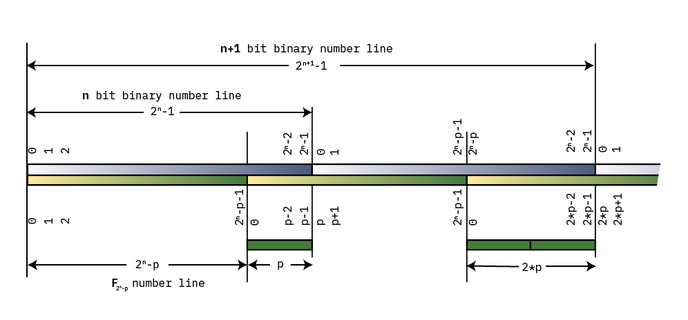
A diagram illustrating modular reduction

The diagram above draws out the number lines for both a simple binary number line, and for some field $\mathbf{{F}}_{{{{2^{{n}}}}-p}}$. Both lines start at 0 on the left, and increment until they roll over. The point at which $\mathbf{{F}}_{{{{2^{{n}}}}-p}}$ rolls over is a distance $p$ from the end of the binary number line: thus, we can observe that $2^{{n}}-1$ reduces to $p-1$. Adding 1 results in $2^{{n}}$, which reduces to $p$: that is, the top bit, wrapped around, and multiplied by $p$.

As we continue toward the right, the numbers continue to go up and wrap around, and for each wrap the distance between the “plain old binary” wrap point and the $\mathbf{{F}}_{{{{2^{{n}}}}-p}}$ wrap point increases by a factor of $p$, such that $2^{{n+1}}$ reduces to $2*p$. Thus modular reduction of natural binary numbers that are larger than our field $2^{{n}}-p$ consists of taking the bits that overflow an $n$-bit representation, shifting them to the right by $n$, and multiplying by $p$.

In order to convince myself this is true, I tried out a more computationally tractable example than $\mathbf{{F}}_{{{{2^{{255}}}}-19}}$: the prime field $\mathbf{{F}}_{{{{2^{{6}}}}-5}} = 59$. The members of the field are from 0-58, and reduction is done by taking any number modulo 59. Thus, the number 59 reduces to 0; 60 reduces to 1; 61 reduces to 2, and so forth, until we get to 64, which reduces to 5 — the value of the overflowed bits (1) times $p$.

Let’s look at some more examples. First, recall that the biggest member of the field, 58, in binary is 0b00_11_1010.

Let’s consider a simple case where we are presented a partial sum that overflows the field by one bit, say, the number 0b01_11_0000, which is decimal 112. In this case, we take the overflowed bit, shift it to the right, multiply by 5:

0b01_11_0000
   ^ move this bit to the right multiply by 0b101 (5)

0b00_11_0000 + 0b101 = 0b00_11_0101 = 53

And we can confirm using a calculator that 112 % 59 = 53. Now let’s overflow by yet another bit, say, the number 0b11_11_0000. Let’s try the math again:

0b11_11_0000
   ^ move to the right and multiply by 0b101: 0b101 * 0b11 = 0b1111

0b00_11_0000 + 0b1111 = 0b00_11_1111

This result is still not a member of the field, as the maximum value is 0b0011_1010. In this case, we need to add the number 5 once again to resolve this “special-case” overflow where we have a binary number that fits in $n$ bits but is in that sliver between $2^{{n}}-p$ and $2^{{n}}-1$:

0b00_11_1111 + 0b101 = 0b01_00_0100

At this step, we can discard the MSB overflow, and the result is 0b0100 = 4; and we can check with a calculator that 240 % 59 = 4.

Therefore, when doing schoolbook multiplication, the partial products that start to overflow to the left can be brought back around to the right hand side, after multiplying by $p$, in this case, the number 19. This magical property is one of the reasons why $\mathbf{{F}}_{{{{2^{{255}}}}-19}}$ is quite amenable to math on binary machines.

Let’s use this finding to rewrite the straight schoolbook multiplication form from above, but now with the modular reduction applied to the partial sums, so it all wraps around into this compact form:

                   |    A2        A1       A0
    x              |    B2        B1       B0
   ------------------------------------------
                   | A2*B0     A1*B0    A0*B0
                   | A1*B1     A0*B1 19*A2*B1
                 + | A0*B2  19*A2*B2 19*A1*B2
                 ----------------------------
                        S2        S1       S0

As discussed above, each overflowed limb is wrapped around and multiplied by 19, creating a number of partial sums S[2:0] that now has as many terms as there are limbs, but with each partial sum still potentially overflowing the native width of the limb. Thus, the inputs to a limb are 17 bits wide, but we retain precision up to 48 bits during the partial sum stage, and then do a subsequent condensation of partial sums to reduce things back down to 17 bits again. The condensation is done in the next three steps, “collapse partial sums”, “propagate carries”, and finally “normalize”.

However, before moving on to those sections, there is an additional trick we need to apply for an efficient implementation of this multiplication step in hardware.

In order to minimize the amount of data movement, we observe that for each row, the “B” values are shared between all the multipliers, and the “A” values are constant along the diagonals. Thus we can avoid re-loading the “A” values every cycle by shifting the partial sums diagonally through the computation, allowing the “A” values to be loaded as “A” and “A*19” into holding register once before the computations starts, and selecting between the two options based on the step number during the computation.


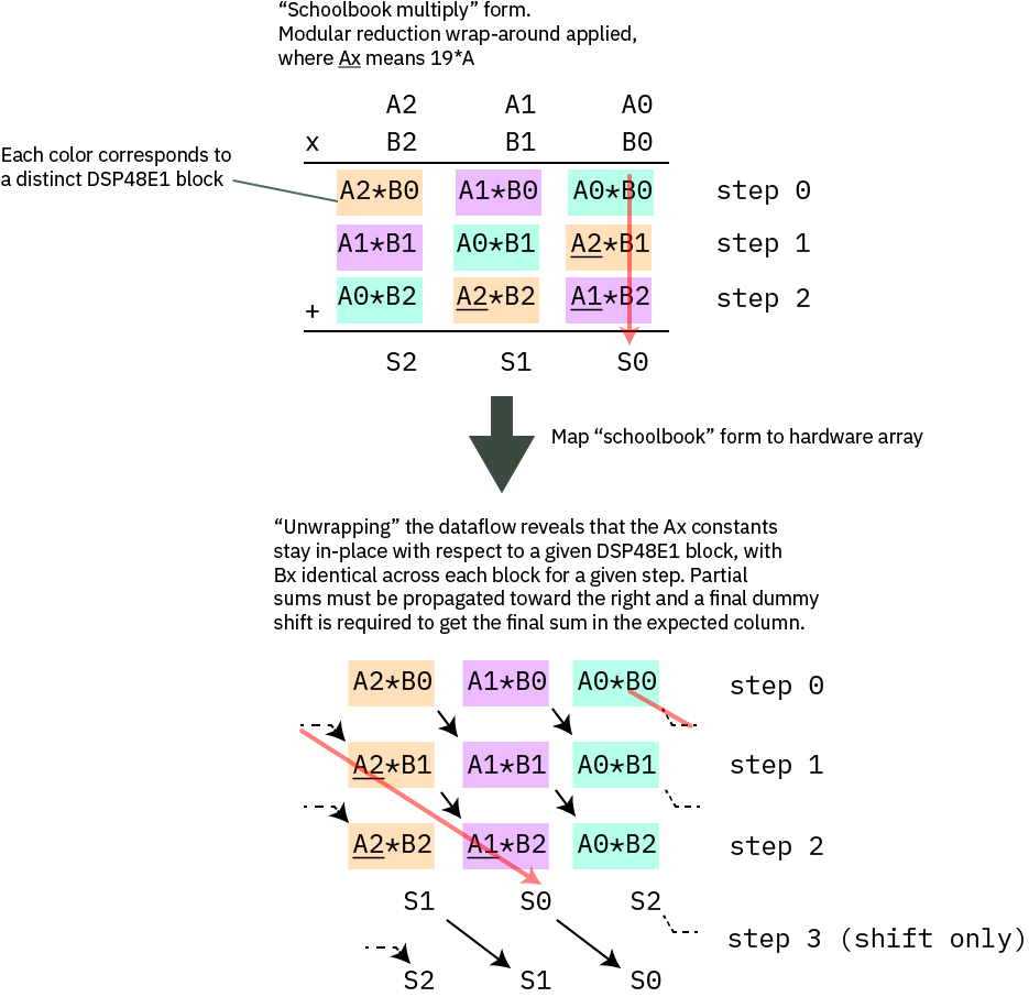
Mapping schoolbook multiply onto the hardware array to minimize data movement

The diagram above illustrates how the schoolbook multiply is mapped onto the hardware array. The top diagram is an exact redrawing of the previous text box, where the partial sums that would extend to the left have been multiplied by 19 and wrapped around. Each colored block corresponds to a given DSP48E1 block, which you may recall is a fast 27×18 multiplier hardware primitive built into our Xilinx FPGAs. The red arrow illustrates the path of a partial sum in both the schoolbook form and the unwrapped form for hardware implementation. In the bottom diagram, one can clearly see that the Ax coefficients are constant for each column, and that for each row, the Bx values are identical across all blocks in each step. Thus each column corresponds to a single DSP48E1 block. We take advantage of the ability of the DSP48E1 block to hold two selectable A values to pre-load Ax and Ax*19 before the computation starts, and we bus together the Bx values and change them in sequence with each round. The partial sums are then routed to the “down and right” to complete the mapping. The final result is one cycle shifted from the canonical mapping.

We have a one-cycle structural pipeline delay going from this step to the next one, so we use this pipeline delay to do a shift with no add by setting the `opmode` from `C+M` to `C+0` (in other words, instead of adding to the current multiplication output for the last step, we squash that input and set it to 0).

The fact that we pipeline the data also gives us an opportunity to pick up the upper limb of the partial sum collapse “for free” by copying it into the “D” register of the DSP48E1 during the shift step.

In C, the equivalent code basically looks like this:

   // initialize the a_bar set of data
   for( int i = 0; i < DSP17_ARRAY_LEN; i++ ) {
      a_bar_dsp[i] = a_dsp[i] * 19;
   }
   operand p;
   for( int i = 0; i < DSP17_ARRAY_LEN; i++ ) {
      p[i] = 0;
   }

   // core multiply
   for( int col = 0; col < 15; col++ ) {
     for( int row = 0; row < 15; row++ ) {
       if( row >= col ) {
         p[row] += a_dsp[row-col] * b_dsp[col];
       } else {
         p[row] += a_bar_dsp[15+row-col] * b_dsp[col];
       }
     }
   }

By leveraging the special features of the DSP48E1 blocks, in hardware this loop completes in just 15 clock cycles.

Collapse Partial Sums

At this point, the potential width of the partial sum is up to 43 bits wide. This next step divides the partial sums up into 17-bit words, and then shifts the higher to the next limbs over, allowing them to collapse into a smaller sum that overflows less.

... P2[16:0]   P1[16:0]      P0[16:0]
... P1[33:17]  P0[33:17]     P14[33:17]*19
... P0[50:34]  P14[50:34]*19 P13[50:34]*19

Again, the magic number 19 shows up to allow sums which “wrapped around” to add back in. Note that in the timing diagram you will find below, we refer to the mid- and upper- words of the shifted partial sums as “Q” and “R” respectively, because the timing diagram lacks the width within a data bubble to write out the full notation: so `Q0,1` is P14[33:17] and `R0,2` is P13[50:34] for P0[16:0].

Here’s the C code equivalent for this operation:

     // the lowest limb has to handle two upper limbs wrapping around (Q/R)
     prop[0] = (p[0] & 0x1ffff) +
       (((p[14] * 1) >> 17) & 0x1ffff) * 19 +
       (((p[13] * 1) >> 34) & 0x1ffff) * 19;
     // the second lowest limb has to handle just one limb wrapping around (Q)
     prop[1] = (p[1] & 0x1ffff) +
       ((p[0] >> 17) & 0x1ffff) +
       (((p[14] * 1) >> 34) & 0x1ffff) * 19;
     // the rest are just shift-and-add without the modular wrap-around
     for(int bitslice = 2; bitslice < 15; bitslice += 1) {
         prop[bitslice] = (p[bitslice] & 0x1ffff) + ((p[bitslice - 1] >> 17) & 0x1ffff) + ((p[bitslice - 2] >> 34));
     }

This completes in 2 cycles after a one-cycle pipeline stall delay penalty to retrieve the partial sum result from the previous step.

Propagate Carries

The partial sums will generate carries, which need to be propagated down the chain. The C-code equivalent of this looks as follows:

   for(int i = 0; i < 15; i++) {
     if ( i+1 < 15 ) {
        prop[i+1] = (prop[i] >> 17) + prop[i+1];
        prop[i] = prop[i] & 0x1ffff;
     }
   }

The carry-propagate completes in 14 cycles. Carry-propagates are expensive!

Normalize

We’re almost there! Except that $0 \leq result \leq 2^{{256}}-1$, which is slightly larger than the range of $\mathbf{{F}}_{{{{2^{{255}}}}-19}}$.

Thus we need to check if number is somewhere in between 0x7ff….ffed and 0x7ff….ffff, or if the 256th bit will be set. In these cases, we need to add 19 to the result, so that the result is a member of the field $2^{{255}}-19$ (the 256th bit is dropped automatically when concatenating the fifteen 17-bit limbs together into the final 255-bit result).

We use another special feature of the DSP48E1 block to help accelerate the test for this case, so that it can complete in a single cycle without slowing down the machine. We use the “pattern detect” (PD) feature of the DSP48E1 to check for all “1’s” in bit positions 255-5, and a single LUT to compare the final 5 bits to check for numbers between {prime_string} and $2^{{255}}-1$. We then OR this result with the 256th bit.

If the result falls within this special “overflow” case, we add the number 19, otherwise, we add 0. Note that this add-by-19-or-0 step is implemented by pre-loading the number 19 into the A:B pipeline registers of the DSP4E1 block during the “propagate” stage. Selection of whether to add 19 or 0 relies on the fact that the DSP48E1 block has an input multiplexer to its internal adder that can pick data from multiple sources, including the ability to pick no source by loading the number 0. Thus the operation mode of the DSP48E1 is adjusted to either pull an input from A:B (that is, the number 19) or the number 0, based on the result of the overflow computation. Thus the PD feature is important in preventing this step from being rate-limiting. With the PD feature we only have to check an effective 16 intermediate results, instead of 256 raw bits, and then drive set the operation mode of the ALU.

With the help of the special DSP48E1 features, this operation completes in just a single cycle.

After adding the number 19, we have to once again propagate carries. Even if we add the number 0, we also have to “propagate carries” for constant-time operation, to avoid leaking information in the form of a timing side-channel. This is done by running the carry propagate operation described above a second time.

Once the second carry propagate is finished, we have the final result.

Potential corner case

There is a potential corner case where if the carry-propagated result going into “normalize” is between

0xFFFF_FFFF_FFFF_FFFF_FFFF_FFFF_FFFF_FFDA and
0xFFFF_FFFF_FFFF_FFFF_FFFF_FFFF_FFFF_FFEC

In this case, the top bit would be wrapped around, multiplied by 19, and added to the LSB, but the result would not be a member of $2^{{255}}-19$ (it would be one of the 19 numbers just short of $2^{{255}}-1$), and the multiplier would pass it on as if it were a valid result.

In some cases, this isn’t even a problem, because if the subsequent result goes through any operation that also includes a reduce operation, the result will still reduce correctly.

However, I do not think this corner case is possible, because the overflow path to set the high bit is from the top limb going from 0x1_FFFF -> 0x2_0000 (that is, 0x7FFFC -> 0x80000 when written MSB-aligned) due to a carry coming in from the lower limb, and it would require the carry to be very large, not just +1 as shown in the simple rollover case, but a value from 0x1_FFED-0x1_FFDB.

I don’t have a formal mathematical proof of this, but I strongly suspect that carry values going into the top limb cannot approach these large numbers, and therefore it is not possible to hit this corner case. Consider that the biggest value of a partial sum is 0x53_FFAC_0015 (0x1_FFFF * 0x1_FFFF * 15). This means the biggest value of the third overflowed 17-bit limb is 0x14. Therefore the biggest value resulting from the “collapse partial sums” stage is 0x1_FFFF + 0x1_FFFF + 0x14 = 0x4_0012. Thus the largest carry term that has to propagate is 0x4_0012 >> 17 = 2. 2 is much smaller than the amount required to trigger this condition, that is, a value in the range of 0x1_FFED-0x1_FFDB. Thus, perhaps this condition simply can’t happen? It’d be great to have a real mathematician comment if this is a real corner case…

Real Hardware

You can jump to the actual code that implements the above algorithm, but I prefer to think about implementations visually. Thus, I created this timing diagram that fully encapsulates all of the above steps, and the data movements between each part (click on the image for an editable, larger version; works best on desktop):

Block diagrams of the multiplier and even more detailed descriptions of its function can be found in our datasheet documentation. There’s actually a lot to talk about there, but the discussion rapidly veers into trade-offs on timing closure and coding technique, and farther away from the core topic of the Curve25519 algorithm itself.

Didn’t You Say We Needed Thousands of These…?

So, that was the modular multiply. We’re done right? Nope! This is just one core op in a sequence of thousands of these to do a scalar multiply. One potentially valid strategy could be to try to hang the modular multiplier off of a Wishbone bus peripheral and shove numbers at it, and come back and retrieve results some time later. However, the cost of pushing 256-bit numbers around is pretty high, and any gains from accelerating the multiply will quickly be lost in the overhead of marshaling data. After all, a recurring theme in modern computer architecture is that data movement is more expensive than the computation itself. Damn you, speed of light!

Thus, in order to achieve the performance I was hoping to get, I decided to wrap this inside a microcoded “CPU” of sorts. Really more of an “engine” than a car — if a RISC-V CPU is your every-day four-door sedan optimized for versatility and efficiency, the microcoded Curve25519 engine I created is more of a drag racer: a turbocharged engine block on wheels that’s designed to drive long flat stretches of road as fast as possible. While you could use this to drive your kids to school, you’ll have a hard time turning corners, and you’ll need to restart the engine after every red light.

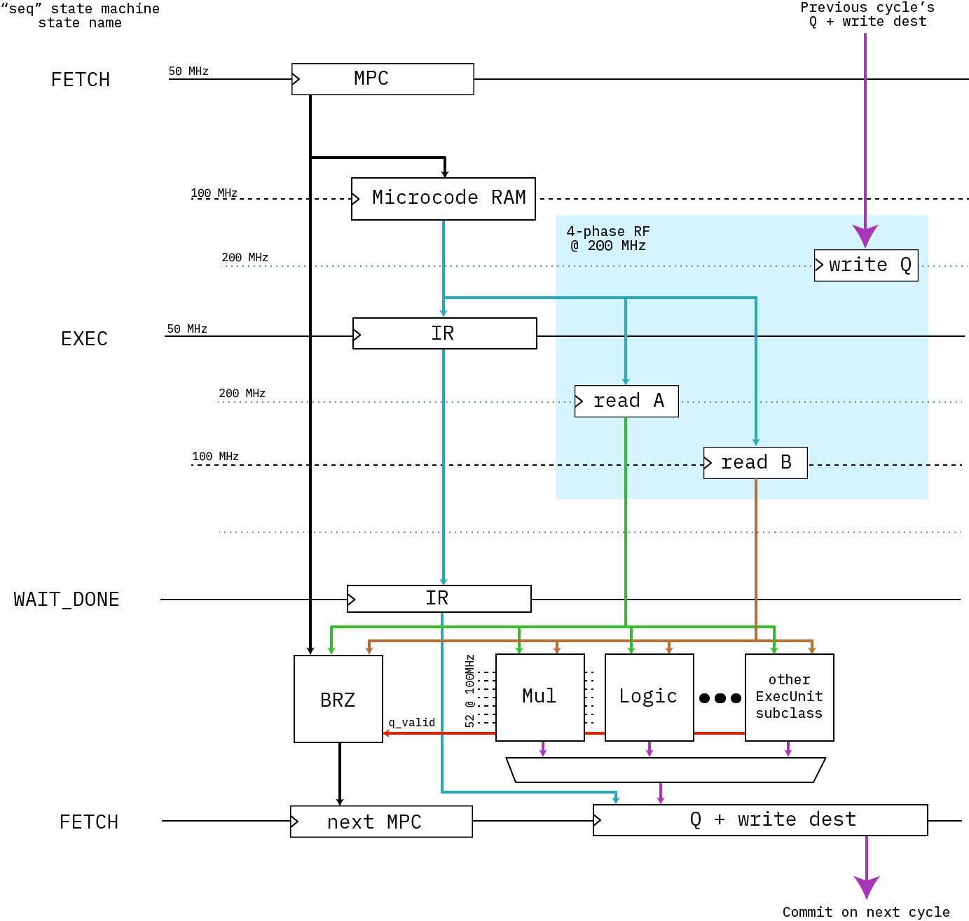
Above is a block diagram of the engine’s microcoded architecture. It’s a simple “three-stage” pipeline (FETCH/EXEC/RETIRE) that runs at 50MHz with no bypassing (that would be extremely expensive with 256-bit wide datapaths). I was originally hoping we could close timing at 100MHz, but our power-optimized -1L FPGA just wouldn’t have it; so the code sequencer runs at 50MHz; the core multiplier at 100MHz; and the register file uses four phases at 200MHz to access a simple RAM block to create a space-efficient virtual register file that runs at 50MHz.

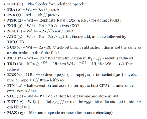
The engine has just 13 opcodes:

There’s no compiler for it; instead, we adapted the most complicated Rust macro I’ve ever seen from johnas-schievink’s rustasm6502 crate to create the abomination that is engine25519-as. Here’s a snippet of what the assembly code looks like, in-lined as a Rust macro:

let mcode = assemble_engine25519!(
start:
    // from FieldElement.invert()
    // let (t19, t3) = self.pow22501();   // t19: 249..0 ; t3: 3,1,0
    // let t0  = self.square();           // 1         e_0 = 2^1
    mul %0, %30, %30  // self is W, e.g. %30
    // let t1  = t0.square().square();    // 3         e_1 = 2^3
    mul %1, %0, %0
    mul %1, %1, %1
    // let t2  = self * &t1;              // 3,0       e_2 = 2^3 + 2^0
    mul %2, %30, %1
    // let t3  = &t0 * &t2;               // 3,1,0
    mul %3, %0, %2
    // let t4  = t3.square();             // 4,2,1
    mul %4, %3, %3
    // let t5  = &t2 * &t4;               // 4,3,2,1,0
    mul %5, %2, %4

    // let t6  = t5.pow2k(5);             // 9,8,7,6,5
    psa %28, #5       // coincidentally, constant #5 is the number 5
    mul %6, %5, %5
pow2k_5:
    sub %28, %28, #1  // %28 = %28 - 1
    brz pow2k_5_exit, %28
    mul %6, %6, %6
    brz pow2k_5, #0
pow2k_5_exit:
    // let t7  = &t6 * &t5;               // 9,8,7,6,5,4,3,2,1,0
    mul %7, %6, %5
);

The `mcode` variable is a [i32] fixed-length array, which is quite friendly to our `no_std` Rust environment that is Xous.

Fortunately, the coders of the curve25519-dalek crate did an amazing job, and the comments that surround their Rust code map directly onto our macro language, register numbers and all. So translating the entire scalar multiply inside the Montgomery structure was a fairly straightforward process, including the final affine transform.

How Well Does It Run?

The fully accelerated Montgomery multiply operation was integrated into a fork of the curve25519-dalek crate, and wrapped into some benchmarking primitives inside Xous, a small embedded operating system written by Xobs. A software-only implementation of curve25519 would take about 100ms per DH operation on a 100MHz RV32-IMAC CPU, while our hardware-accelerated version completes in about 6.7ms — about a 15x speedup. Significantly, the software-only operation does not incur the context-switch to the sandboxed hardware driver, whereas our benchmark includes the overhead of the syscall to set up and run the code; thus the actual engine itself runs a bit faster per-op than the benchmark might hint at. However, what I’m most interested in is in-application performance, and therefore I always include the overhead of swapping to the hardware driver context to give an apples-to-apples comparison of end-user application performance. More importantly, the CPU is free to do other things while the engine does it’s thing, such as servicing the network stack or updating the UX.

I think the curve25519 accelerator engine hit its goals — it strapped enough of a rocket on our little turtle of a CPU so that it’ll be able render a chat UX while doing double-ratchets as a background task. I also definitely learned more about the algorithm, although admittedly I still have a lot more to learn if I’m to say I truly understand elliptic curve cryptography. So far I’ve just shaken hands with the fuzzy monsters hiding inside the curve25519 closet; they seem like decent chaps — they’re not so scary, I just understand them poorly. A couple more interactions like this and we might even become friends. However, if I were to be honest, it probably wouldn’t be worth it to port the curve25519 accelerator engine from its current FPGA format to an ASIC form. Mask-defined silicon would run at least 5x faster, and if we needed the compute power, we’d probably find more overall system-level benefit from a second CPU core than a domain-specific accelerator (and hopefully by then the multi-core stuff in Litex will have sufficiently stabilized that it’d be a relatively low-risk proposition to throw a second CPU into a chip tape-out).

That being said, I learned a lot, and I hope that by sharing my experience, someone else will find Curve25519 a little more approachable, too!

Adding a ChaCha Cipher to Precursor’s TRNG

Tuesday, June 22nd, 2021

This is the second post of a two-part series on Betrusted/Precursor’s True Random Number Generator (TRNG).

A bulletproof source of random numbers is a key component of any cryptosystem, so we’ve done an extensive, months-long characterization of Precursor’s dual, redundant TRNG sources, which consists of an avalanche noise generator and a ring oscillator. We’ve found them to produce passable raw entropy, but you don’t have to take my word for it. You can download our raw data and run your on analysis on it if you like (at least until our ISP cuts us off for serving multiple 10GiB files filled with random data).

However, the system is still missing two features that are generally considered to be best practice:

  1. Independent, on-line health monitors of the raw TRNG outputs, discussed in our previous post.
  2. Conditioning of the raw data.

Because Precursor uses an FPGA for its SoC, we can add new features to the hardware “on the fly”, and in this post will focus on adding the hardware for the conditioning of raw data. The post is a bit of a slog to read through; I’ll try not to do too many in this style. But occasionally, I think it’s good to have a “reality check” that conveys the depth of difficulties encountered while implementing a feature, instead of making everything look easy or cramming all the details into a tweet. This post will hopefully also serve as a detailed reference for the handful of future developers who want to implement similar features, and would like to avoid some of the mistakes I’ve made.

Despite best efforts to make TRNGs unbiased and flawless, they are really hard to get right. Furthermore, they are only capable of producing high-quality entropy at a limited data rate. Thus, most practical systems take a TRNG output and run it through a cryptographic stream cipher to generate a final datastream; this conditioning of the raw data simultaneously protects against minor flaws in the TRNG while improving the availability of entropy.

So in Precursor, we’d like to add some conditioning on the collected entropy. To be clear, we will always make the raw entropy pool available for inspection — this is absolutely necessary for testing and CI coverage — but it’s a good idea to throw the output of your TRNG into a cryptographically sound stream cipher of some type, so that in the case that your TRNG suffers a sporadic drop-out, you don’t have a disastrous, instantaneous collapse of entropy. Depending on how you configure the conditioning, you can also increase the effective availability of random numbers.

After poking around a bit on the Internet, it seems popular to feed a seed of entropy into the ChaCha20 stream cipher (I refer to it as a “cipher” in this post, but I think more technically because of the way I’m using it, it should be referred to as a CSPRNG – Cryptographically Secure Pseudo Random Number Generator). This is done in the Linux kernel as well as by cryptech.is’s HSM and a few other implementations. The devil, of course, is always in the details. Cryptech.is takes the output of their TRNGs, hashes them with a SHA2 block, and then feeds it into a ChaCha20 stream cipher. Linux maintains an entropy pool that is collected from a variety of low-and-high-quality sources, blends them using some fast and slow techniques based upon the nature of the source, runs it through SHA1, and then into ChaCha20 to create the final stream.

In our implementation, we’re skipping the SHA pre-hash of the entropy pool, for the following reasons:

  1. We don’t have the space (as in FPGA gates) or computational resources (as in CPU cycles for software emulation) to do this continuously
  2. The raw entropy sources themselves are fairly high-quality (as opposed to in the case of Linux they are taking things like time stamps and network traffic patterns, so using SHA-1 to blind that is quite reasonable); and, we have two entropy sources of different architectures, each source consisting of multiple raw entropy generation elements. In other words, we’re starting from a pretty good place already.
  3. The ChaCha20 cipher is mainly to protect against transient drop-out or unpredicted aging issues in the TRNG.
  4. The ChaCha20 cipher itself is considered to be cryptographically secure; augmenting it with a SHA pre-hash does not seem to lend any clear benefit in our case.
  5. We will prefer to reseed the ChaCha20 cipher at a fairly high rate, rather than seed it occasionally through a more expensive SHA operation.

Also in reading some of the docs out there, it seem that 20 is the minimum number of rounds considered to be cryptographically secure for ChaCha, but “more rounds is better”. Thus, while tweaking the Secworks open-source Chacha implementation to fit in Precursor, I think I’ll also create an option to let the ChaCha rounds function run to at least a minimum number of rounds but otherwise “free run” when the system is idle. This makes it useless as a cipher, but if the power impact is minimal, this should help the diffusion of entropy across all the bits of the cipher and make it more robust against attempts to back-track its state.

The diagram above gives an “artist’s impression” of the architecture of the system. It’s an early sketch, before I fully understood everything going on. The final details came out a little different, but the big ideas are there. Not shown is logic that ensures the ChaCha20 cipher has completed its minimum amount of rounds between each output sample, and automatic re-seeding logic that pulls in 32 bits of entropy from the TRNGs on a regular basis at some re-seeding interval that can be programmed by software.

After installing the tooling necessary to build a Precursor/Betrusted SoC and run simulations, I started writing the code.

Here’s the general method I use to develop code:

  1. Think about what I’m trying to do. See above.
  2. Write the smaller submodules.
  3. Wrap the smaller modules into a simulation framework that shakes most of the skeletons out of the closet.
  4. Repeat 1-3, working your way up the chain until you arrive at your full solution.
  5. Write drivers for your new feature
  6. Slot your feature into the actual hardware
  7. Test in real hardware
  8. Continuously integrate, if possible, either by re-running your sim against every repo change or better yet recompiling and re-running your test on actual hardware.

The key to this loop is the simulation. The better your simulation, the better your outcome. By “better simulation”, I mean, the less assumptions and approximations made in the test bench. For example, one could simulate a module by hooking it up to a hand-rolled set of Verilog vectors that exercises a couple read and write cycles and verifies nothing explodes; or, one could simulate a module by hooking it up to a fully simulated CPU, complete with power-on reset and multiple clock phases, and using a Rust-based framework to exercise the same reads and writes. The two test benches ostensibly achieve the same outcome, but the latter checks much more of the hairy corner cases.

For Betrusted/Precursor, we developed a comprehensive simulation framework that achieves the latter scenario as much as possible. We simulate a full, gate-level VexRISCV CPU, running a Rust-built BIOS, employing as many of the Xilinx-provided hardware models as we can for things like the PLL and global power-on reset. You can make a new testbench by running the “new_sim.py” script in the `deps/gateware/sim` directory, and it will automatically copy over all the basics so you can just instantiate your core module and start running simulation code.

Another thing I learned perhaps too late was to pick a good IDE. Python sucks to develop. It sucks even more without an IDE. For a long time I was writing in vanilla emacs. The game-changer for me was being able to control-click through modules and find their definitions; most IDEs support this.

Writing The Block

I noted in Cryptech.is’s presentations that they were using a 24-round variant with a potential to go to 32; and even though cryptanalysis shows its solid with 20 rounds, perhaps there is still a potential that maybe some knowledge of the output could be used to infer something about the next set of outputs.

So, I still made a very light-fingered change, where the core round function could be advanced by one during idle periods based on a `force_round` input. In any case, the output of the ChaCha cipher is not used until at least 20 rounds in any case, but on average it will go many more rounds (thousands of rounds) before the output is used, and the number of rounds advanced depends upon the exact timing of the code that accesses the TRNG.

Thus, the overall flow of events for the conditioning block are as follows:

  1. On boot, we pull in 384 bits of “key” state (256 bits key + 64 bits iv + 64 bits nonce) from the TRNG, and then initialize the cipher.
  2. We also pull in 512 bits of “input” state. This is a fixed quantity that is XOR’d with the ChaCha block state. I worry that tying this to a fixed value could lead to leakage of the ChaCha state to the output, thus, on every boot we load in a new random input value.
  3. Once the cipher is initialized, a counter keeps track of how many blocks we’ve generated. Once we have passed a threshold, the conditioner automatically requests another 32-bit word of entropy from the TRNG and does a rotate-and-XOR of the data into the “key” state. The key state is re-incorporated on the next “advance” call of the block.
  4. Every “selfmix” interval, the cipher will also advance its rounds counter by one (this is the supplemental entropy/scrambling as noted previously)
  5. The user can also supply seeding data at any time, which is folded in with a rotate-and-XOR function. Note for every seed provided, it’s best practice to read 16 words of TRNG output, to ensure that the seed state is incorporated into the TRNG as a whole. It doesn’t harm things to not do that, just, if you kept on applying the same seed over and over again it’ll eventually just XOR into and out of the key pool without doing anything useful.
  6. The output of the cipher is latched into a 512-bit register, and `urandom` data outputs are multiplexed to the kernel and userspace through the CSR. A `valid` bit is provided, and it should be checked prior to every read of data from the Conditioned TRNG output.

Building, and Failing

So your code is all writ, now time to try a quick “smoke test” to see if the build fails. And, sure enough, even though the build completes, I’m not meeting timing. We’re using a -1L variant of the Spartan 7 part, which is the lowest power model (important for battery life) but also the slowest performer in the group. So, even though Cryptech.is advertised hitting 100MHz performance on the block, I did note they were using a -3 variant (one of the fastest models) of a fairly high-end Artix FPGA.

So, back to the drawing board — it’s time to drop the clock frequency on the core to 50MHz. This is probably fine from a performance standpoint, as it could still yield 1.6Gbps burst rate of random numbers, but it does introduce some potentially thorny issues with clock domain crossings. In particular, I don’t get to be lazy and just use a bunch of Migen’s BusSynchronizer primitives to bridge 512-bit data between domains. That would be…expensive, in terms of logic resources. Instead, I’m going to have to be careful and use multi-cycle paths with explicit timing exceptions to make sure this works and without consuming undue amounts of resources.

What — you mean you thought getting code to compile was the end of the story? In hardware, every flip flop is a race condition against a clock — just think of it that way. Every time you make a register, you now have a potential concurrency problem. Now scale that up to the tens of thousands of registers in an FPGA, and you get an idea of why correct compilation is only a small portion of the whole story.

Failing More, in Order to Get Better

After reducing the frequency of the core to 50MHz and fighting for a half day with the Vivado constraints syntax to convince it not to spend half an hour routing cross-clock-domain that are actually relaxed, I finally have the design building with timing closure. The next step is going back into the simulation bench and checking all the corner cases.

I modified the existing `trng_managed` simulation bench to add a series of tests that would exercise all the new features — including checking the rate of read, all the dual port options, and deliberately forcing some reads to fail by bypassing certain checks on validity of data to really push the engine to its limit. In the process of running these benches, I found more new corner cases, for example, the ChaCha engine would stall if the raw entropy FIFO ran out of seeding data; it would just wait for reboot of the avalanche+ring oscillator TRNGs, a process that can take milliseconds. This shouldn’t happen on the `urandom` engine — it is the “unlimited” random data engine after all, so some fixes were made to keep the block state evolving even if we ran out of seeding data. However, I have to emphasize this really is a corner case, you have to basically configure the system to constantly reseed and pull entropy out at a rate much higher than you can do anything useful with it to hit that limit. But, that’s the point of testing — to break your system before users do.

Rinse, Lather, Repeat

Now that the simulation runs, we repeat the loop and see how badly timing is broken. It turns out with all the tweaks in place, I’ve introduced an accidental critical path. While the design can meet timing with this, it takes almost 3x the time to build, which means we’re probably going to start failing builds pretty soon. I should probably fix this problem now, while the design details are fresh in my head.

I open up the design in the Vivado tools and have it plot a timing histogram for me, below is an example of the output:

Above: Example of a slack histogram generated by Vivado. Green bars toward the left indicate paths with less timing slack, to the right have more. So for example, the left-most bin has 206 paths with 0.041ns-0.227ns of slack. The more “left-heavy” the histogram is, the harder the design is to place & route, and the more likely the process will not complete with perfect timing closure.

The left-most bin are the most over-constrained elements, and I can see that the `trngmanaged_holding_buf` registers are just barely passing.

I generate a schematic view like this inside the Vivado design tool, and backtracing the inputs to the `holding_buf` registers I can see the signal eventually goes through an enormous combinational path that includes the VexRiscV’s address decoders. This means that we have a critical path that extends from inside the VexRiscV load/store unit all the way to the 512-bit shifter of the ChaCha block.

If it were the case that we actually needed to pull data cycle-by-cycle out of the ChaCha block and somehow change the behavior of the system within a single cycle, then this path would make sense. But in practice, the actual rate is far lower than that — the tightest, most unrolled read loops take at least 2 cycles to execute; but more typically 10-12 cycles per iteration if you’re doing any sort of useful load or store with the data and running it from a rolled-up loop. Furthermore, the ChaCha block is basically a “read-only” block — there’s nothing the CPU is going to do to reconfigure it on the fly that would prevent us from
pipelining this.

So, I go back and add a “depth 1 FIFO” to the output, to break the shift register out of the critical path while still preserving the read-invalidate semantics required by the CSR interface (that is, the contract we have with the CSR interface is the cycle after a random number is read, either the next value should be a valid, new random number; or it can be an invalid number, but the “valid” bit must be cleared that very cycle). Using a simple pipeline register won’t work, because it introduces an extra cycle delay on the read-invalidate semantics and it’s possible, although very unlikely, that a code loop could have back-to-back loads and it will grab a stale “valid” state.

After running another simulation just to make sure we haven’t introduced any new bugs, I run a compilation again and hope this greatly relaxes the timing. It didn’t, but long story short, I had accidentally leaked one path in the FIFO through as a combinational element. After spending a couple hours tracing that issue out, I finally met with some success.

After applying these fixes, the compilation time is back down to its normal value, and we can see that the timing bins at the very far left of the histogram have a fraction of paths as before — 69, down from 206. It looks like the `holding_buf` register is still causing some troubles, but at least we’ve taken pressure off of the actually most difficult paths, which are inside the Curve 25519 Engine, and not some made-up timing emergencies inside the shift register at the output stage of the TRNG.

The price of all the timing fixes is increased resource utilization. Initial estimates showed about a 6% area cost for the ChaCha block without the timing fixes, but we ended up with around 10.5% area cost once all is said and done. The SoC uses around 68.2% of the FPGA now, which is still fine for routability and gives some space for a few more smaller blocks, but it’s probably at the upper limit of what we can reasonably expect to fit while having short (~8-9 minute) compilation cycles. I’m also making a mental note to myself that as part of the histogram analysis it looks like the next critical path to knock back is in the CSR address decoders. Adding the dozens of registers to read out the results from the TRNG health tests has probably forced an extra layer of LUTs to be instantiated inside the core arbitration logic; thus, pruning some of these registers if they end up being superfluous could be a way to win back some timing margin if I end up in a jam later.

Rubber, Meet Road. Road, Meet Rubber.

Well, that took some time in simulation. But we’re not done yet! It’s time to run this code on real hardware, and then upgrade the kernel and services of Xous to use it — and let’s not forget CI integration as well.

First things first, let’s just take the design, as-is, with no mods to Xous and see if it boots, and what the power draw change is. The good news is that things boot, and the system draws about 5 mA extra, or about 5% more idle power than it did before. The ChaCha whitener is in the always-on domain, because it has to be able to run while the kernel is idling to produce random data. In particular, the core can “wake up” the avalanche generator and ring oscillators while the CPU is idle to summon more TRNG data even when the CPU is asleep; as such its clock can’t be gated off, but it is better than the alternative of running the CPU to manage these processes. A quick test tweaking the knobs on the duty cycle of the self-mixing for the ChaCha core shows it doesn’t have a measurable impact on the power, which means that probably most of the extra power is just the fixed cost of clocking that much more logic on the fabric.

The next step is to switch over the kernel and core services from using raw random numbers to the new ChaCha conditioned “urandom” source. This should have been easy in theory since everything worked in simulation, but of course — it didn’t work. I was greeted with a full system hang on the first go. This kind of bug is dreaded, because it’s some issue in the full system integration that exists outside of the testbenches, so you have to resort to long compile cycles and “printf” debugging.

Some further poking revealed that even worse yet, on some boots, the system worked, on others, it didn’t. However, the pattern was enough for me to suspect an issue in the reset logic. Going back into my code, I did find a subtle bug where I forgot to assign the reset line for the ChaCha core to the 50MHz clock domain (it was still tied to the reset for the 100MHz clock domain). For good measure, I also added a reset pulse extender, just to make sure it saw a long, solid reset. The polarity of the ChaCha core reset is opposite from what the rest of the system uses, so it’s also possible there is some glitches due to that. Anyways, after another four hours of tweaking and testing these fixes, re-running simulations, and cross-checking documentation about the reset process to really make sure we found a root cause, the system seems to come up as expected from the “urandom” source.

For TRNGs, The Work is Never Done

The final phase of modifying any TRNG is continuous integration. This is extremely important because you can only get a hint if a TRNG is mis-behaving in subtle ways after collecting dozens of gigabytes of data from it over dozens of runs; and due to the limited rate of entropy, gathering such quantity of data can take weeks. Thus, we have a Precursor unit dedicated to doing nothing but rotating through its entropy sources and feeding its data into a set of test suites to try and uncover any subtle biases in the generators. You can browse the raw data and results of our CI bench here.

Now that we have this conditioned output, we need to integrate that into the test bench. It’s also going to be important to do a few “cold boot with recorded data” runs as well, so we can compare boot-to-boot to make sure that we have actually seeded the generator with random data and we’re not just accidentally running a ChaCha cipher (which should have excellent statistical randomness) with a fixed set of keys (which would have an identical stream boot-to-boot despite the excellent statistics).

In the process of re-integrating these tests into the CI bench, I discovered a number of problems with our original tool for shuttling random numbers to the host for analysis. For a number of reasons, the original CI tool relied on a fairly complicated Rust program with multiple threads, which was getting hard to maintain and the Rust wasn’t adding a lot of value; in fact I found a subtle integration bug that was causing all the tests for the past month to be run only on the ring oscillator!

Since we had a pretty decent Python script for doing USB updates over USB, I modified that into a script currently living in xous-core/tools/trng_test.py. This script is matched to a thread that runs inside the `trng` server on the Xous side when it is built with one of the TRNG tester options. On the Precursor side, a pair of 512kiB buffers are filled and the host is told which of the two to read from. The host-side Python script then reads the buffers and echos its contents out as binary data to stdout, which can then by piped into an analysis program (such as `dieharder`) or recorded to disk for later analysis. This whole mess is then wrapped in some other shell-script Frankenstein that’s fired off by a cron job which manages the rebuild, reflashing, and logging of data via a Raspberry Pi that can keep an eye on the serial console for errors during the CI process. It feels like a house made of playing cards, but it works!

Closing Thoughts

If you made it this far, congratulations. Hopefully it conveys, with some accuracy, the range of difficulties one might encounter when implementing a “typical” feature like this for an FPGA-based SoC, and it may even be useful to the handful of developers who want to actually attempt something like this!