Archive for the ‘betrusted’ Category

Evaluating Precursor’s Hardware Security

Monday, November 23rd, 2020

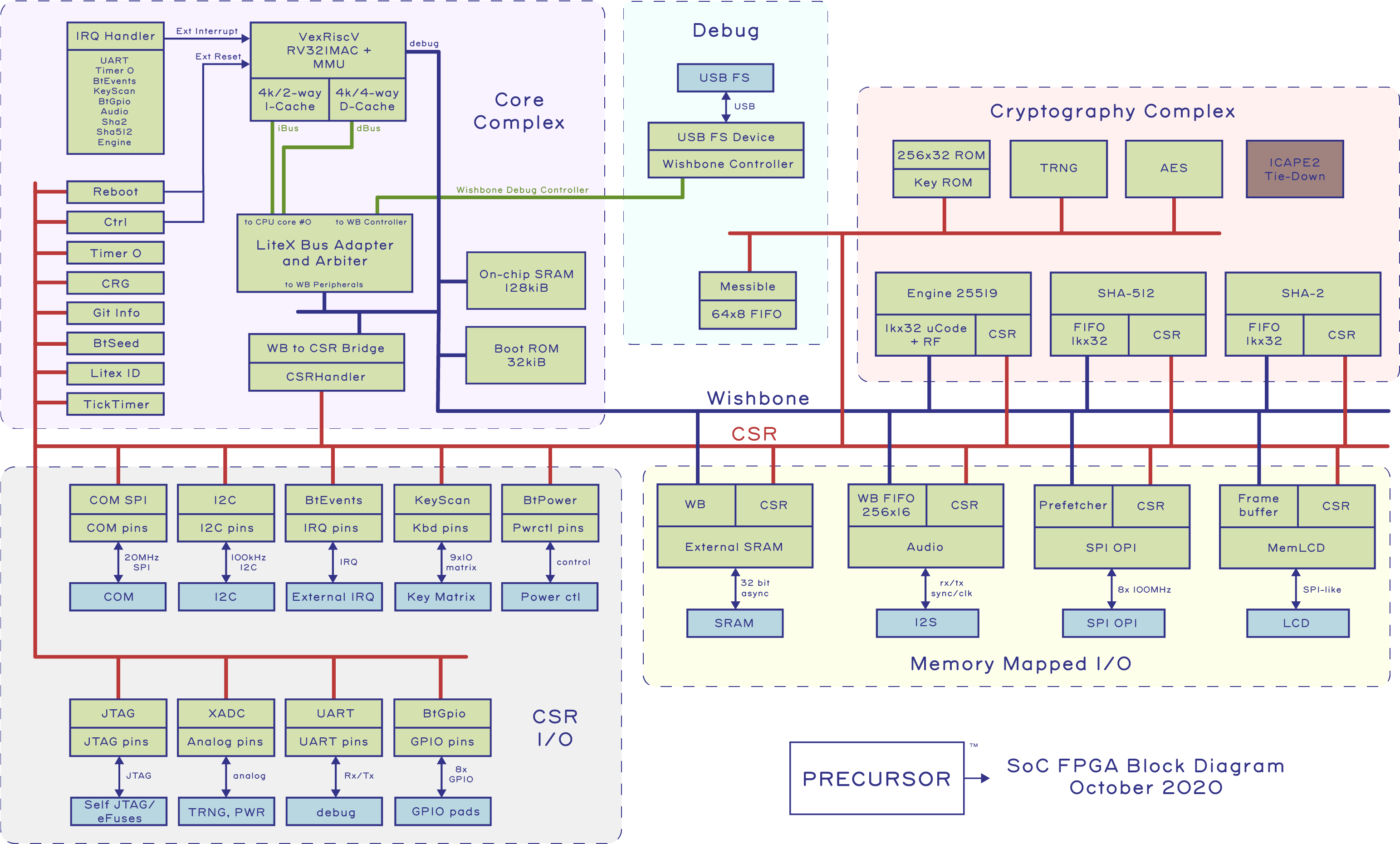
Making and breaking security go hand in hand. I’ve talked a lot about how Precursor, a mobile hardware development platform for secure applications, was made. In this post, I try to break it.

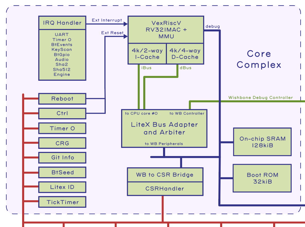
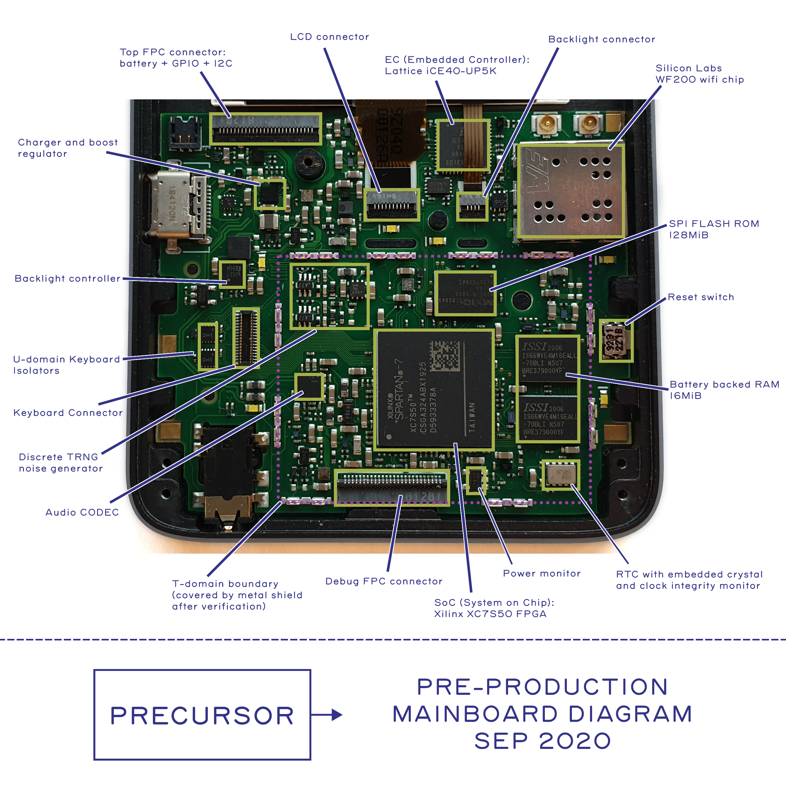
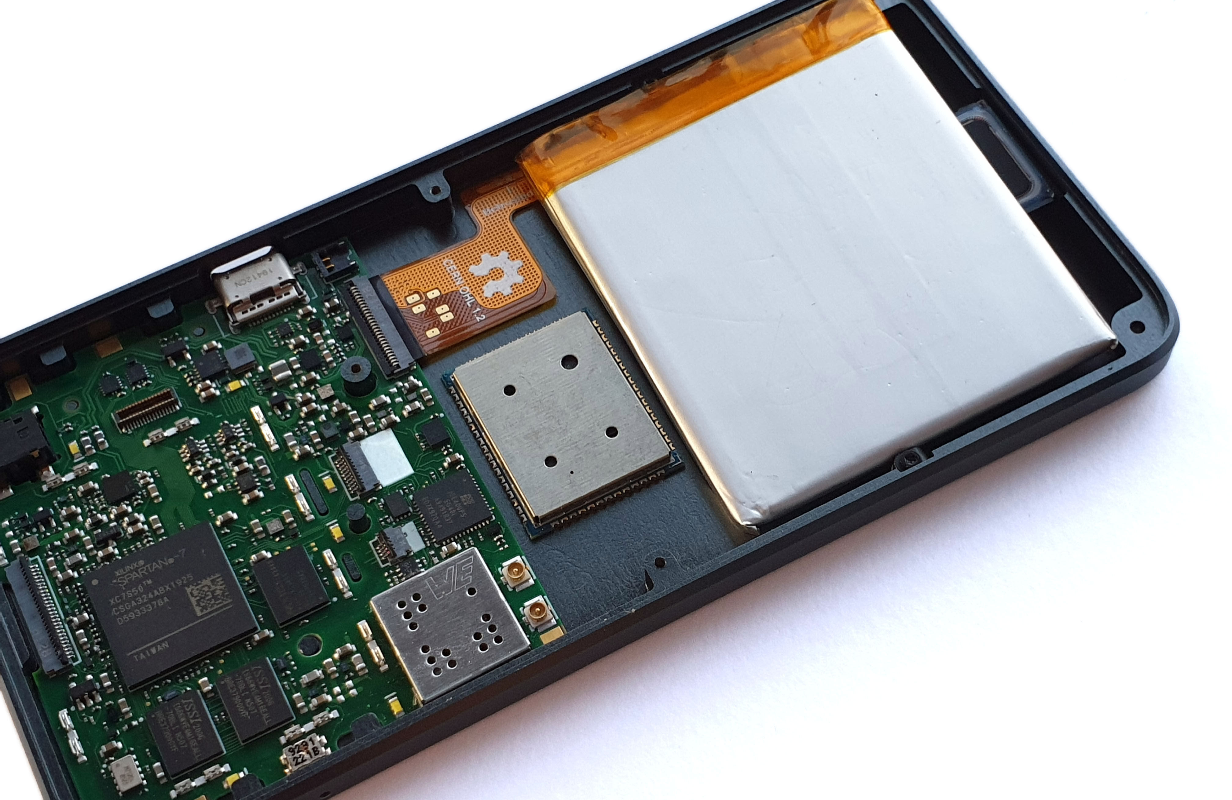
Hardware security is a multi-faceted problem. First, there is the question of “can I trust this piece of hardware was built correctly?”; specifically, are there implants and back doors buried in the hardware? We refer to this as the “supply chain problem”. It is a particularly challenging problem, given the global nature of our supply chains, with parts pulled from the four corners of the world, passing through hundreds of hands before reaching our doorstep. Precursor addresses this problem head-on with open, verifiable hardware: the keyboard, display, and motherboard are easy to access and visually inspect for correct construction. No factory or third-party tool is ever trusted with secret material. Precursor is capable of generating its own secret keys and sealing them within the hardware, without additional tools.

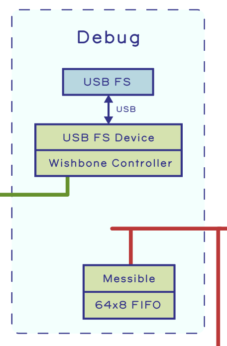
We also use a special kind of logic chip for the CPU – an FPGA – configured by the user, not the factory, to be exactly the CPU that the user specified. Crucially, most users have no evidence-based reason to trust that a CPU contains exactly what it claims to contain; few have the inspection capability to verify a chip in a non-destructive manner. On the other hand, with an FPGA, individual users can craft and inspect CPU bitstreams with readily available tools. Furthermore, the design can be modified and upgraded to incorporate countermeasures against hardware exploits discovered in the FPGA’s underlying fabric. In other words, the current trustability situation for an ASIC-style CPU is basically “I surrender”, whereas with an FPGA, users have the power to configure and patch their CPUs.


See my previous post for more details on how an FPGA helps solve the problem of transparency in CPU designs

Trustable hardware is only one facet of hardware security. Beyond correct construction, there are also questions of “has anyone tampered with the hardware while I wasn’t looking?”, and “can my hardware keep its secrets if it falls into the wrong hands?” These are the “tamper evidence” and “tamper resistance” problems, respectively. The rest of this post will drill down into these two questions as they relate to Precursor.

Despite any claims you may have heard otherwise, tamper resistance is a largely unsolved problem. Any secrets committed to a non-volatile format are vulnerable to recovery by a sufficiently advanced adversary. The availability of near-atomic level microscopy, along with sophisticated photon and phonon based probing techniques, means that a lab equipped with a few million dollars worth of top-notch gear and well-trained technicians has a good chance of recovering secret key material out of virtually any non-volatile storage media. The hard part is figuring out where the secrets are located on the chip. Once this is known for a given make and model, the attack is easy to repeat. This means the incremental cost of recovering keys from a previously studied design is in the ballpark of $10k’s and a matter of days. For some popular types of silicon packaging, such as flip chips, so-called “back side probing” techniques may be able to non-destructively extract secret key material within a matter of hours.


Ptychographic X-ray imaging as referenced in this article reveals the detailed 3-D structure of a modern chip.

Keys stored in volatile memory – that is, battery-backed RAM – can significantly up the ante because any disruption of power to the key memory can disrupt its data. Cryogenic freezing of the circuitry can help preserve the data for readout in the event of power loss, but battery-backed key storage can also incorporate active countermeasures to detect environmental anomalies and reactively zeroize the keys. While this sounds great for storing extremely sensitive secrets, it’s also extremely risky because false triggers can erase the keys, millions of dollars of cryptocurrency could vanish with a single false move. Thus volatile keys are best suited for securing highly sensitive but ephemeral communications and not for the long-term storage of high-value secrets.

Tamper evidence, not to be confused with tamper resistance, is the ability of a secured hardware device to show evidence of tampering. An example of very basic tamper evidence is the “warranty void if removed” sticker. It is typically placed over a screw essential to holding the case together, so that any attempt to disassemble the unit requires puncturing the sticker. This very basic measure is easily defeated by duplicating and replacing the sticker, and it’s not hard to acquire even the holographic stickers if you know the right people.

The next level up in tamper evidence is the incorporation of a physically unclonable feature in the tamper-evident seal, such as meauring the random pattern of fibers in the paper of the sticker, or recording the position of glittery bits embedded in nail polish applied over a seam. Of course, none of these physical features can attest to any evidence of side-channel attacks, which do not require opening the case. In the case of side channel attacks, adversaries can gain enough information about secrets contained within a piece of hardware by just observing patterns in the power consumption or in the spurious radio waves emitted from the hardware. Attackers can also induce transient faults with the hope of tricking a device into disclosing secrets without breaking through labels by exposing the hardware to high levels of radiation or temperature extremes. Depending on the threat model, the hardware may simply need to hamper such attacks, or it may need to react to them and take appropriate action depending upon the nature of the attack.

Because hardware security is hard, the lack of a known exploit should never be taken as the existence of strong security. We take this fact to heart in Precursor: in addition to putting effort into designing a trustable, secured hardware solution, we have also put effort into exploiting it. Unlike most other secure hardware vendors, we also tell you about the exploits in detail, so you can make an informed decision about the practical limits of our implementation’s tamper evidence and resistance.

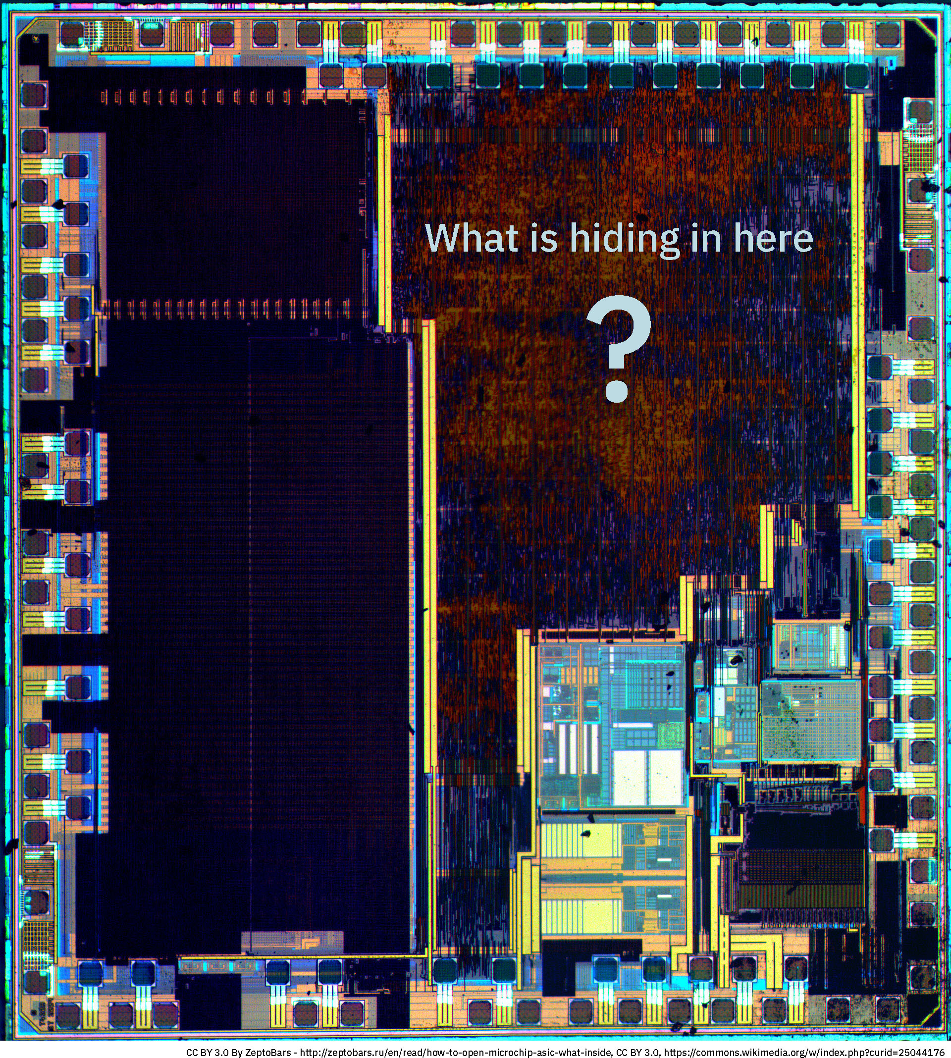
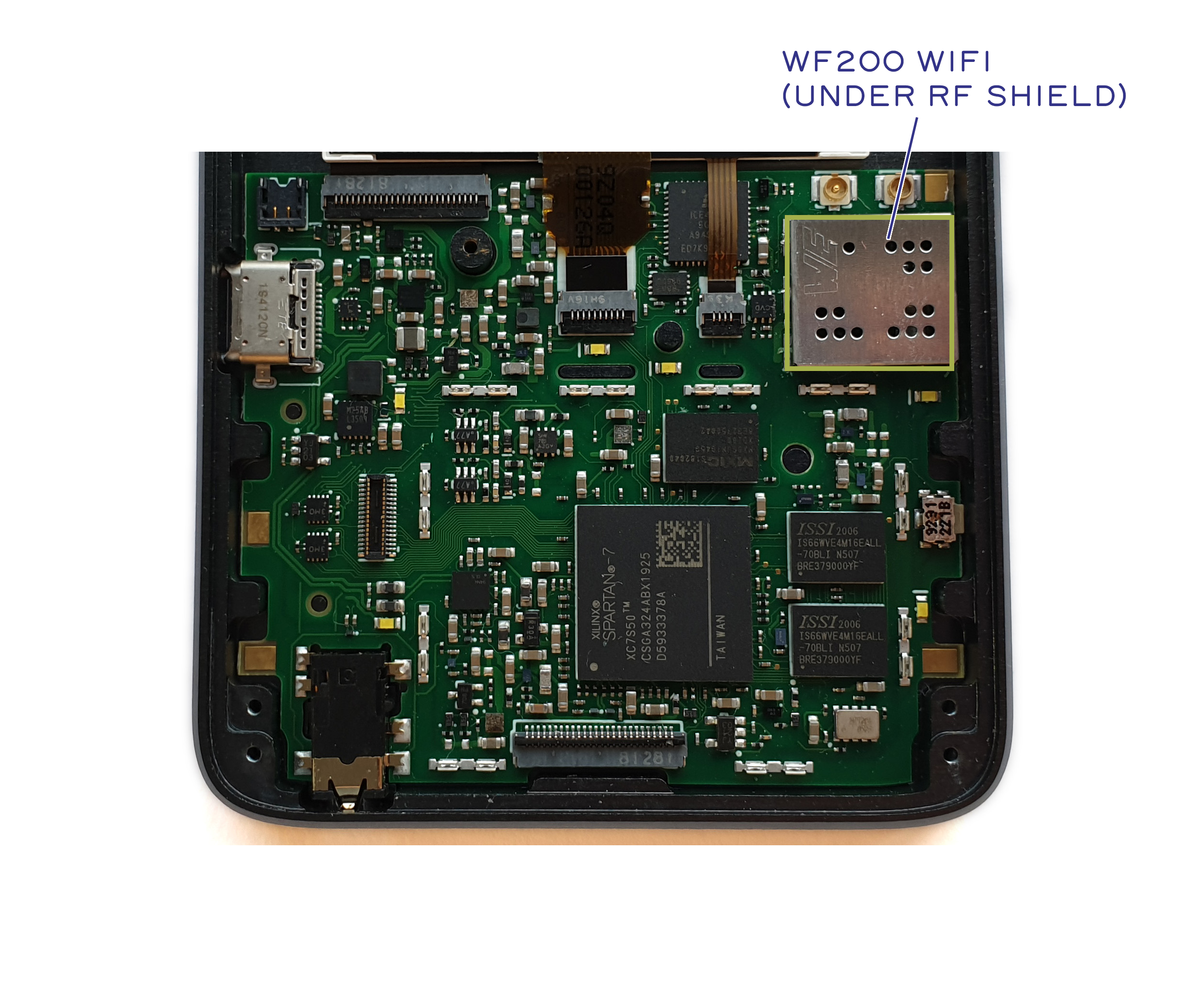
Precursor uses the Xilinx 7-series of FPGAs for its trusted root. This series of FPGAs is perhaps one of the most extensively studied from a security perspective; dozens of papers have been published about its architecture and vulnerabilities. As a result, its key stores have been reverse engineered and analyzed down to the transistor level.


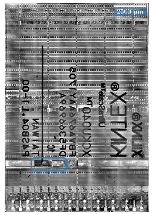
An example of the analysis done by other researchers on the 7-Series FPGAs

The most serious known vulnerability in the chip was published in early 2020, by Maik Ender, Amir Moradi, and Christof Paar in a paper titled “The Unpatchable Silicon: A Full Break of the Bitstream Encryption of the 7-Series FPGAs”. In a nutshell, it allows an attacker equipped with nothing more than the ciphertext of the bitstream and access to the FPGA’s JTAG port to recover the plaintext of a bitstream. It relies on a feature known as the WBSTAR register, normally used to recover from a corrupted boot. By design, it loads a recovery address from a location encrypted in the bitstream, and places the address in a register that is necessarily disclosed to the boot media to set a new loading location for the fallback image. Unfortunately, the “recovery address” is just a piece of data at the pointy end of an unchecked pointer. This means it can be used to fetch one word of plaintext from anywhere in the bitstream. The attack also takes advantage of the malleability of AES CBC blocks to adjust the WBSTAR load offset, thus allowing the FPGA to be used as an “oracle” to decrypt ciphertext one word at a time, without any knowledge of the encryption key.

The paper suggested a mitigation involving a pair of pins on the FPGA that change value based on the contents of the WBSTAR register to trigger a key reset (assuming you’ve stored the key in battery-backed RAM and not burned it permanently into the chip). While trying to implement the proposed mitigation, we found several ways to easily circumvent it. In particular, the external pin update is not automatic, it is done by an additional command later in the bitstream. By just omitting the pin updating command, we can render this mitigation ineffective without affecting the ability to read out the plaintext. We have published the code necessary to reproduce this attack in our jtag-trace github repository.

This means that the tamper resistance of Precursor is equivalent to the strength of the glue applied over the SPI ROM chip and the JTAG port. The glue on the SPI ROM chip hampers the recovery of the ciphertext, necessary for the attack, while gluing the JTAG port shut hampers the upload of exploit code. Furthermore, the ciphertext should be treated as a secret, as knowledge of it is necessary for recovery of the plaintext. Therefore, the FPGA should still be burned with an encryption key and set to only accept encrypted bitstreams. This is because JTAG readout of the SPI ROM ciphertext can only happen with the help of a bitstream specifically crafted for the purpose. As long as such a bitstream is not encrypted to the secret key inside the FPGA, the ciphertext should be unavailable through the JTAG port.

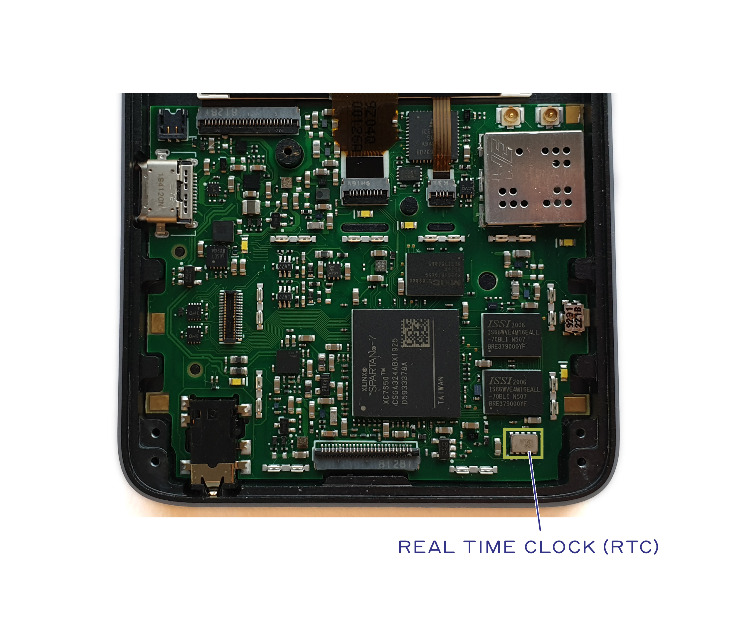
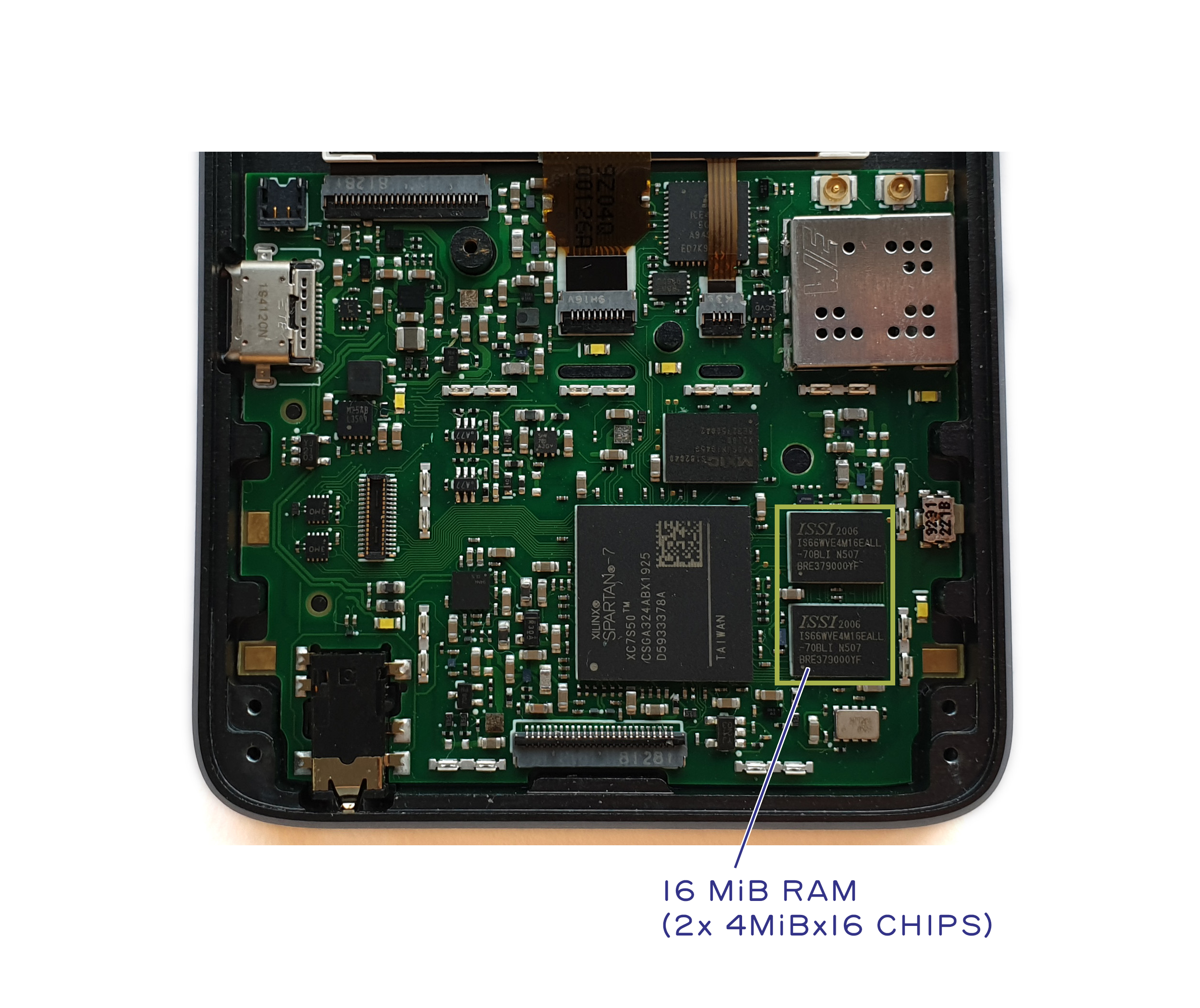
Based on this evaluation, we’re planning on implementing the circuitry necessary to zeroize RAM-backed encryption keys, but not for the purpose of directly mitigating this exploit. Unfortunately, a separate oversight in the security features of the 7-Series means devices that boot from BBRAM must also accept unencrypted bitstreams. Therefore access to ciphertext is much easier on BBRAM-keyed devices than on devices that boot from fused keys. However, by including the BBRAM key zeroization circuitry, users could at least have a choice of which type of key (battery-backed or fused) to use, depending on their risk profile. Battery-backed keys complicate any hardware attack by requiring the hardware to receive uninterrupted power as it is disassembled, in exchange for the risk of key loss in case the user forgets to keep the battery charged. Fortunately, the power needed to preserve the key is miniscule, lower than the self-discharge current of the battery itself. It’s also useful for users who wish to have a “self-destruct timer” or “panic button” to completely, securely, and irrevocably wipe their devices in a fraction of a second. This is useful for protecting high-value secrets that have a short or pre-determined lifetime.


A schematic of Precursor’s proposed BBRAM key zeroization circuit. It is a pair of back-to-back NMOS-style inverters, which latches the system into a shutdown state until the battery is removed. There are additional circuits provisioned to rapidly discharge key-related voltage rails, not shown here.

Once Precursor has been glued shut, we propose the easiest method to recover the ciphertext and to gain access to the JTAG ports is to put the Precursor device into a precision CNC milling machine, mill out the PCB from the back side, and then place the remaining assembly into a pogo-pin based mechanism to perform the readout. This of course destroys the Precursor device in the process, but it is probably the most direct and reliable method of recovering the encryption keys, as it is very similar to an existing technique used for certain types of attacks on iPhones. Storing keys in BBRAM can greatly complicate the task of milling out the PCB by creating a high risk of accidental key erasure, but a sufficiently precise CNC with a non-conductive ceramic bit, or a precision laser-based ablation milling system can reduce the risk of key loss substantially. Cryogenic cooling of the FPGA chip itself may also help to preserve key material in the case of very short accidental power glitches.


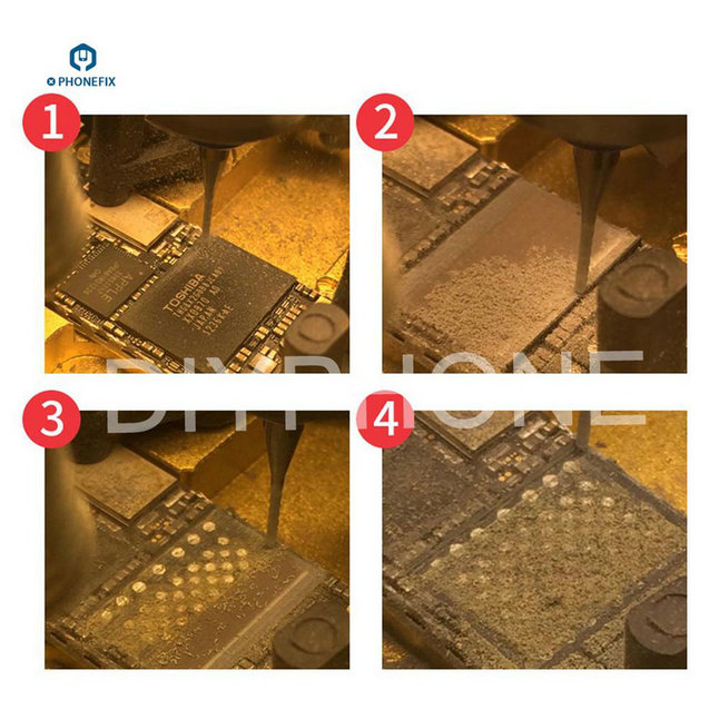
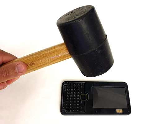
CNC milling machines can be used to perform precision attacks on dense circuit boards. Above is a vendor demo of a CNC milling bit removing a NAND chip from an iPhone motherboard, without damage to adjacent components. The mill can be readily purchased for a couple thousand USD.

The level of equipment and skill required to execute such attacks is higher than available in a typical Makerspace or government field office, but could be made available within a specialized lab of any modern intelligence agency or large technology corporation. Of course, if Precursors became a popular method to store high-value secrets, an entrepreneurial hacker could also start a lucrative service to recover keys from devices with just a couple hundred thousand dollars in startup capital.

That being said, such an attack would likely be noticed. In other words, if your device is functional and its seals intact, your Precuror has probably not been tampered with. But, if it is confiscated or stolen, you can assume its secrets could be extracted in as little as a few hours by a well-prepared adversary. This is not ideal, but this barrier is still higher than countless other “secured systems” ranging from from game consoles to smartphones to crypto wallets that can be broken with nothing more than a data cable and a laptop. Of course, these “easy breaks” are typically due to a bug in the firmware of the device, but unlike most of these devices Precursor’s firmware is patchable, as well as being completely open for audit.

To assist users with gluing their Precursors shut, we include an easy-to-mix two-part epoxy in the box so that users may “pot” their boards once they have inspected their device and are satisfied it meets their standard for correct construction. Remember, we don’t seal the boards in the factory because that makes it impossible for users to confirm no back doors were inserted into the hardware. Upon completing inspection of the hardware, we recommend users perform the following actions to permanently seal their Precursor systems:

  1. Instruct the Precursor firmware to self-generate and burn an AES encryption key to the device, re-encrypt the FPGA bitstream to this key, and finally burn the fuse preventing boot from any other source.
  2. Disassemble the unit and snap the provided metal lid onto the motherboard. In addition to making it more difficult to physically access the hardware, it absorbs radio waves, thus making RF-based attacks more difficult.
  3. Hand-draw a memorable object or word onto a piece of tissue paper that is about 2.5 cm (1 inch) square.
  4. Use a cotton swab to drip the provided two-part clear epoxy through the holes of the RF shield, especially over the debug connector and SPI ROM.
  5. Lay the tissue paper over the wet epoxy, allowing the paper to become saturated with the epoxy.
  6. Wait 24 hours for the epoxy to dry, and re-assemble for use.


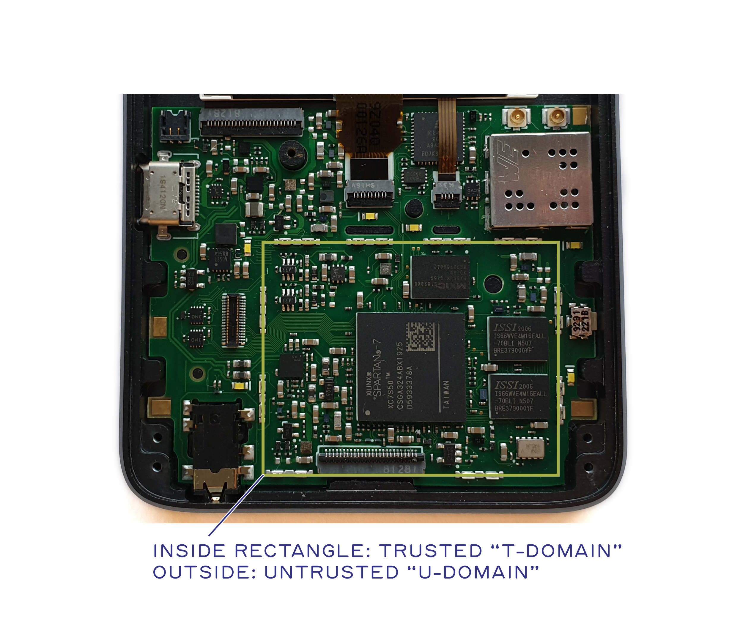
Precursor is designed to have the “Trusted” zone covered with a metal shield that can be glued down with epoxy.

The main risk of applying the epoxy is it leaking onto a connector that should not be glued down. The board is laid out to avoid that outcome, but caution is still needed during sealing. Pouring too much glue into the metal lid can result in glue leaking onto connectors that should not be sealed, preventing re-assembly. Notably, the sealing is done at the user’s risk; once a sealing attempt has been made, we can’t repair or replace a unit since the epoxy is unremovable by design.

The purpose of the tissue paper is to provide a simple but memorable way to confirm the uniqueness of your Precursor unit. It relies upon a human’s innate ability to recognize drawings or lettering made with their own hand. This method allows verification of the seal with simple visual inspection, instead of relying upon a third party tool to, for example, record and analyze the position of glitter dots or paper fibers for authenticity.

We provide Epotek 301 “Bi-packs” as the two-part epoxy for potting Precursor devices. It is commonly used for encapsulating optoelectronics and semiconductors such as LEDs and sensors. As such, it has excellent electrical properties, good optical clarity, robust mechanical durability, and a suitable viscosity for penetrating the nooks and crannies of small electronic parts. Once cured, any attempt to physically access the electronics contained within will leave some kind of mark as evidence of the attempt.

The Precursor device has a well-characterized hardware security level. We’ve designed the hardware to be easier to inspect and seal, so you have an evidenced-based reason to trust the hardware. As all devices are vulnerable to hardware tampering, we’ve taken the approach of preferring devices with well-characterized vulnerabilities. We picked the Xilinx 7-Series FPGAs in part because it has been studied for years: its fuse boxes and encryption engine have been analyzed down to the gate level and there have been no findings so far reporting special access modes for law enforcement, undocumented shadow key stores, or other bugs that could lead to fully remote exploits or back doors. We’ve also taken the time to reproduce and disclose the known vulnerabilities, so that you don’t have to trust our statements about the security of the hardware: you’re empowered to reproduce our findings and make your own evidence-based findings about the trustworthiness of Precursor. In parallel with Precursor, the Betrusted project aims to raise the bar even higher, but doing so will require fabricating a custom ASIC, which incidentally carries its own set of verifiability and supply chain risks that we hope to address with countermeasures that are beyond the scope of this post.

In the end, there is no such thing as perfect security, but we firmly believe that the best mitigation is an evidence-based ecosystem built around the principles of openness, transparency, and lots and lots of testing. If you’re interested in participating in our ecosystem, please visit the Precursor crowdfunding page.

What is a System-on-Chip (SoC), and Why Do We Care if They are Open Source?

Tuesday, November 10th, 2020

Note: This post originally appeared as an update in the crowdfunding campaign for Precursor.

Modern gadgets are typically built around a single, highly integrated chip, known as a “System on Chip” (SoC). While the earliest home computer motherboards consisted of around a hundred chips, Moore’s Law pushed that down to just a handful of chips by the time 80286 PC/AT clones were mainstream, and the industry has never looked back. Now, a typical SoC integrates a CPU core complex, plus dozens of peripherals, including analog, RF, and power functions; there are even “System in Package” solutions available that package the SoC, RAM, and sometimes even the FLASH die into a single plastic package.

Modern SoCs are exceedingly complex. The “full user’s manual” for a modern SoC is thousands of pages long, and the errata (“bug list”) – if you’re allowed to see it – can be hundreds of pages alone. I put “full user’s manual” in quotations because even the most open, well-documented SoCs (such as the i.MX series from NXP) require a strict NDA to access thousands of pages of documentation on third party Intellectual Property (IP) blocks for functions such as video decoding, graphics acceleration, and security. Beyond the NDA blocks, there is typically a deeper layer of completely unpublished documentation for disused silicon, such as peripherals that were designed-in but did not make the final cut, internal debugging facilities, and pre-boot facilities. Many of these disused features aren’t even well-known within the team that designed the chip!

Disused silicon is a thing because building chips is less like snapping together Legos, and more like a sculptor chiseling away at a marble block: adding a circuit is much harder than deactivating a circuit. Adding a circuit might cost around $1 million in new masks, while delaying the project by about 70 days (at a cost of 100,000 man-hours worth of additional wages); with proper planning, deactivating a circuit may be as simple as a code change, or a small edit to a single mask layer, at a cost of perhaps $10,000 and a few days (assuming wafers were held at intermediate stages to facilitate this style of edit).


photo credit: “Man With Mallet & Chisel Bas Relief (Washington, DC)” by takomabibelot is licensed under CC BY 2.0

Thus a typical SoC mask set starts with lots of extra features, spare logic, and debug facilities that are chiseled away (disused) until the final shape of the SoC emerges. As Michelangelo once said “every block of stone has a statue inside it, and it is the task of the sculptor to discover it,” we could say “every SoC mask set has a datasheet inside it, and it is the task of the validation team to discover it”. Sometimes the final chisel blow happens at boot: an errant feature may be turned off or patched over by pre-boot code that runs even before the CPU executes its first instruction. As a result, even the best documented SoCs will have a non-trivial fraction of transistors that are disused and unaccountable, theoretically invisible to end users.

From a security standpoint, the presence of such “dark matter” in SoCs is worrisome. Forget worrying about the boot ROM or CPU microcode – the BIST (Built in Self Test) infrastructure has everything you need to do code injection, if you can just cajole it into the right mode. Furthermore, SoC integrators all buy functional blocks such as DDR, PCI, and USB from a tiny set of IP vendors. This means the same disused logic motifs are baked into hundreds of millions of devices, even across competing brands and dissimilar product lines. Herein lies a hazard for an unpatchable, ecosystem-shattering security break!

Precursor sidesteps this hazard by implementing its SoC using an FPGA. FPGAs are user-reconfigurable, drastically changing the calculus on the cost of design errors; instead of chiseling away at a block of marble, we are once again building with a Lego set. Of course, this flexibility comes at a cost: an FPGA is perhaps 50x more expensive than a feature-equivalent SoC and about 5-10x slower in absolute MHz. However, it does mean there is no dark matter in Precursor, as every line of code used to describe the SoC is visible for inspection. It also means if logic bugs are found in the Precursor SoC, they can be patched with an update. This drastically reduces the cost to iterate the SoC, making it more economically compatible with an open source approach. In an ideal world, the Precursor SoC design will be thoroughly vetted and audited over the next couple of years, converging on a low-risk path toward a tape out in fixed silicon that can reduce production costs and improve performance all while maintaining a high standard of transparency.

LiteX: The Framework Behind Precursor’s SoC

Precursor’s SoC is built using LiteX. LiteX is a framework created by Florent Kermarrec for defining SoCs using the Migen/MiSoC FHDL, which itself is written in Python 3.6+. The heart of LiteX is a set of “handlers” that will automatically adapt between bus standards and widths. This allows designers to easily mix and match various controllers and peripherals with Wishbone, AXI, and CSR, bus interconnect standards. It is pretty magical to be able to glue an extra USB debug controller into a complex SoC with just a few lines of code, and have an entire infrastructure of bus arbiters and adapters figure themselves out automatically in response. If you want to learn more about LiteX and FPGAs, a great place to start is Florent’s “FPGA_101” mini-course.

A Brief Tour of Precursor’s SoC


Above is a block diagram of Precursor’s SoC, as of October 2020. It’s important to pay attention to the date on documentation, because an FPGA-based SoC can and will change over time. We generally eschew pretty, hand-drawn block diagrams like this because they are out of date almost the day they are finished. Instead, our equivalent of a “programmer’s manual” is dynamically generated by our CI system with every code push, and for Rust programmers we have a tool, svd2utra that automatically translates SVD files generated by LiteX into a Rust API crate. With an open source FPGA-based SoC, automated CI isn’t merely best practice, it’s essential, because small but sometimes important patches in submodule dependencies will regularly affect your design.

Core Complex

The “Core Complex” currently consists of one RISC-V core, implemented using Charles Papon’s VexRiscV. We configured it to support the “RV32IMAC” instruction subset, gave it an MMU, and beefed up the caches. The VexRiscV limits cache size to 4kiB, but effective capacity can be increased by upping the cache associativity. We get about a 10% performance boost by tuning the core to have a two-way I-cache, and a four-way D-cache. We also provision a 32 kiB boot ROM, which currently holds three instructions, but will someday be expanded to include signature checks on code loaded from external memory and a 128kiB on-board SRAM for tightly coupled/higher security operations. The CPU core is adapted to, and arbitrated into, a multi-controller Wishbone bus by LiteX and further adapted into a CSR bus by a dedicated CSR bridge that has been configured to automatically space peripherals on 4-kiB page boundaries, so that they can be individually remapped with the MMU. There’s also an IRQ handler that manages interrupts originating from peripherals sprinkled around the chip.

The Core Complex also includes a set of mostly boilerplate CSRs which perform the following functions:

  • “Reboot” allows us to specify a new location for the reset vector
  • “Ctrl” allows us to issue a soft reset
  • “Timer 0” is the default timer provided by LiteX. It is a high resolution 32-bit timer clocked at the same frequency as the CPU core.
  • “CRG” is an interface to control the FPGA’s clock generator. Right now we don’t do much with it, but eventually this is going to play a central role in power management and extending battery life.
  • “Git Info” is a static register that provides information about the state of the git repo from which Precursor was built.
  • “BtSeed” is a 64-bit number that can be randomized to force entropy into the place-and-route process, in case the end user desires a final FPGA netlist unique to their device without having to modify the code (otherwise the builds are entirely reproducible).
  • “Litex ID” is a human-readable text string that identifies the SoC design.
  • “TickTimer” is a low-resolution, 64-bit timer clocked in 1 ms increments. It serves as a source of time for the Xous OS.

Debug Block

Adjacent to the Core Complex is a Debug block. The Debug block features a full speed USB MAC/PHY that can tunnel Wishbone packets and serve as an alternate Wishbone controller to the CPU. We use this to drive the debug interface on the CPU, thus allowing GDB to connect to Precursor over USB even when the CPU is halted. In fact, one could build Precursor with no RISC-V CPU and just tunnel Wishbone packets over USB for debug and driver development. The debug block also includes a small CSR peripheral called the “Messible”, which is a 64-entry by 8-bit wide FIFO, useful as a mailbox/scratchpad during debugging.

Memory Mapped and CSR I/O

The memory space of the RISC-V CPU is mapped onto various peripherals and memory blocks via a Wishbone bus. For traditional SoC designers, Wishbone is kind of like AXI, but open source. Wishbone supports fancy features like multiple masters, pipelining, and block transfers. A portion of the Wishbone bus space is further mapped onto a bus called the Configuration and Status Register (CSR) bus.

While Wishbone is high-performance, it requires more interface logic and is happiest when the peripheral’s bit width matches the bus width. CSRs are area-efficient and gracefully accommodates registers of arbitrary bit-width from both a hardware and software API standpoint, but are lower performance. Thus CSRs are ideal for low-to-medium speed I/O tasks (such as the eponymous configuration and status registers), whereas Wishbone is ideal for memory-mapped I/O where improved bandwidth and latency are worth the area overhead.

From a design process, most peripherals start life mapped to CSR space, and are then upgraded to a memory-mapped implementation to meet performance demands. Thus, it’s no coincidence that most peripherals on Precursor are CSR-only devices. Here is a brief description of each CSR peripheral. As a reminder, you can always consult our reference manual for more details.

  • “COM SPI” is the SPI bus that connects to the Embedded Controller (EC) SoC. It’s a 20MHz SPI peripheral that has a fixed transfer width of 16-bits. This block is targeted for an upgrade to a memory mapped I/O block.
  • “I2C” is an I2C bus controller. Currently, only a real time clock (RTC) chip and an audio CODEC chip are are connected to this I2C bus.
  • “BtEvents” is a catch-all block for handling various external real-time interrupt sources. Currently it handles interrupts from the EC and RTC chips.
  • “KeyScan” is the keyboard controller. It’s designed to scan a 9×10 keyboard matrix for key hits, using a slow external 32kHz clock source. By decoupling the keyboard scanner from the system core clock, the system can go to a lower power state while waiting for keyboard presses, extending the number of days that Precursor can go between charges.
  • “BtPower” is a set of GPIOs dedicated specifically to managing power. It can turn the audio and discrete TRNG on and off, override the EC’s power control commands, activate boost mode for the USB type C port (allowing operation as a DFP or “host”), and engage the self-destruct mechanism.
  • “JTAG” is a set of GPIOs looped back to the FPGA’s JTAG pins. These are used in combination with our eFuse API drivers to self-provision AES bitstream encryption fuses on the 7 Series FPGA.
  • “XADC” is the interface for the 7-Series XADC block, which is a 12-bit, multi-channel ADC. This is primarily used for the self monitoring of system voltages. In the final production revision, at least one channel of the ADC will also be available as a configuration option on the GPIO internal header so that users have an easier path to integrating analog sensors into Precursor.
  • “UART” is a simple 115200, 8-N-1 serial interface which is connected to the debug header for console I/O.
  • “BtGpio” is a straight-forward digital I/O block for driving the pins on the GPIO internal header. Note that due to the nature of the FPGA’s implementation, it’s not possible to switch between a digital GPIO function and an analog GPIO function without updating the bitstream.

In addition to the CSR I/Os, a few I/O devices are memory-mapped for high performance:

  • “External SRAM” is a 32-bit wide, asynchronous interface that memory-maps 16 MiB of external SRAM. The SRAM is battery-backed so that it can retain state while the SoC is powered off. The intention is to optimize power by reducing sleep/wake overhead. However, this also means that the self-destruct procedure must first clear sensitive data from SRAM before activating the final blow that knocks out the SoC, as the self-destruct circuitry is also powered by the SRAM’s backup power supply. The External SRAM block also has a CSR interface to read out the configuration mode of the SRAM.
  • “Audio” is an I2S interface to an external audio CODEC. In addition to a CSR block that configures the I2S interface, it also includes a pair of 256×16 entry memory-mapped sample FIFOs.
  • “SPI OPI” is a high-speed SPI-like interface to external FLASH storage that memory-maps 12 8MiB of non-volatile storage. The “O” in OPI stands for octal – it’s an 8-bit bus that runs at 100MHz DDR speeds. It also includes a pre-fetcher that can hold several cache line’s worth of code, optimizing the case of straight-line code execution. High performance on this bus is essential, since the intention is for the CPU to run most code as XIP out of FLASH. It also features a CSR interface to control operations like block erase and page programming.
  • “MemLCD” is the frame buffer for the LCD. The Sharp Memory LCD contains its own internal memory, which allows it to retain an image even when the host is powered off. The MemLCD frame buffer is thus a cache for the LCD itself. It manages which lines of the LCD are dirty and will flush only the dirty lines to the LCD upon requests made via the CSR. This improves the perceived update rate of the LCD, which is limited to 10 Hz if the entire screen is being updated, but improves inversely proportional to the fraction of the screen that is static.

Cryptography Complex

All the features described thus far consume about 20% of the FPGA’s logic; the majority of the logic in Precursor’s FPGA is dedicated to the Cryptography Complex.

Above is an amoeba plot that visualizes the relative size of various functions within the Precursor SoC design. Some blocks, such as the semi-redundant SHA-512 and SHA-2 accelerators, are currently included simply because we could fit both of them in the FPGA, and not because we strictly needed both of them. Fortunately, removing the SHA-2 block is as easy as commenting out four lines of code, saving about 2800 SLICE LUTs or about 9% of the device’s resources. LiteX and the svd2rust scripts take care of everything else!

Here’s a quick run-down of the blocks inside the Cryptography Complex:

  • “Engine25519” is an arithmetic accelerator for operations in the prime field 2^255-19. It’s a microcoded, 256-bit arithmetic engine capable of computing a 256-bit multiply plus normalization in about one microsecond, about a 30x speedup over running the equivalent code on the RISC-V CPU. It consumes a huge amount of resources, but was deemed essential because the Betrusted secure communications application is built around the Double-Ratchet Algorithm, which relies heavily on this type of math. The CI documentation is probably the best starting point to understand more about the Engine25519 implementation. The block is big enough that later on it will get an entire post dedicated to explaining its function.
  • “SHA-512” and “SHA-2” are hardware-accelerated SHA hash blocks. They are derived from Google’s OpenTitan SystemVerilog source code. The SHA-2 block is directly from OpenTitan and included mostly because it was easy to integrate. The SHA-512 block is our own adaptation of the SHA-2 block. This is the historical reason for why we have both in the current build of Precursor, even though most applications will only need one hash or the other to be hardware accelerated.
  • “AES” is an AES accelerator also lifted directly from the Google OpenTitan project. It is capable of doing AES 128, 192, and 256, and supports encryption and decryption in ECB, CBC, and CTR modes.
  • “KeyROM” is a 256×32 ROM implemented using fixed-location LUTs in the FPGA. Since the ROM’s location is fixed, we can use PrjXray to determine the location of the KeyROM bits in the FPGA’s bitstream. This allows us to edit the key ROMs directly into the FPGA bitstream, thus enabling a transfer of trust from the low-level eFuse AES key into the higher-level functions of the Precursor SoC. We will discuss more about some important, recently-discovered vulerabilities in the FPGA eFuse AES key in a post coming soon.
  • “TRNG” is an on-chip, ring oscillator-based TRNG. It uses multiple small rings to collect entropy which are then merged into a single large ring for final measurement. The construction and validation of Precursor’s TRNGs will also get their own post at some point down the road.
  • “ICAPE2” is an explicit tie-down for an unused internal debug port in the FPGA fabric. ICAPE2 is Xilinx’s way of allowing an FPGA to introspect and access internal configuration state. We explicitly tie it down so that no other functions can try to claim it. Also, since the ICAPE2 is at a well-known location in the bitstream, it is possible to write a tool that does post-compilation inspection of the bitstream to verify that the ICAPE2 block is in fact deactivated.

Parting Thoughts

That’s it for our whistle-stop tour of the Precursor SoC! We’ve sculpted in the parts that are essential to functionality and security and hope the development community will add more. By commenting out a few lines of code, you can clear out unnecessary blocks and make space for your own creations. Precursor’s code base is entirely open and available for inspection – no hidden test logic or microcode blobs and no NDA required to trace an unambiguous, cycle-accurate path from the release of reset to the execution of the first instruction. This lack of “dark matter” and total transparency of design adds yet another argument in the evidence-based case to trust Precursor’s hardware with your private matters.

If you enjoyed this post, please check out Precursor’s campaign page for more details and project updates!

Guided Tour of the Precursor Motherboard

Friday, September 25th, 2020

We talk a lot about “verifiable hardware”, but it’s hard to verify something when you don’t know what you’re looking at. This post takes a stab at explaining the major features of the Precursor motherboard by first indicating the location of physical components, then by briefly discussing the rationale behind their curation.

Above is a photo of a pre-production version of Precursor, annotated with the location of key components. Like software, hardware has revisions too. So, when verifying a system, be sure to check the revision of the board first. The final production units will have a clear revision code printed on the back side of every board and we’ll tell you where to look for the code once the location is finalized. There will be a few changes to the board before production, which we’ll talk about later on.

But what do all the components do, and how are they connected? Above is a block diagram that tries to capture the relationship between all the components.

Trusted and Untrusted Domains

First and foremost, you’ll notice that the design is split into two major domains: the “T-domain” and the “U-domain”. “T” stands for “Trusted”; “U” stands for “Untrusted”. A simplified diagram like this helps to analyze the security of the system, as it clearly illustrates what goes into and out of the T-domain; in other words, it defines the hardware attack surface of the trusted domain. Of course, not shown explicitly on the diagram are the side-channels, such as RF emissions and power fluctuations, which can be used to exfiltrate secret data. Very briefly, RF emissions are mitigated by enclosing the entire T-domain in a Faraday cage. Meanwhile, power fluctuations are mitigated partially through local filtering and partially through the use of constant-time algorithms to perform sensitive computations.

As the “Trusted” name implies, the T-domain is where the secrets go, while the U-domain acts as a first-level firewall to the untrusted Internet. The U-domain is explicitly designed for very low power consumption, so that it can be “always on” while still providing several days of standby time. We refer to the FPGA inside the U domain as the Embedded Controller (EC), and the FPGA inside the T-domain as the System on Chip (SoC) or sometimes simply as “the FPGA”.

Power Management and the Embedded Controller (EC)

The intention is that the always-on EC listens for incoming wifi packets; only once a valid packet is received will the T-domain be powered on.

Using a low-power EC separate from the SoC allows power-hungry processing to be done in bursts, after which the T-domain powers itself off. Thanks to the “memory LCD” that we have chosen, the display can appear persistently even when the T-domain is powered down. Of course, leaving data on the screen while the T-domain is powered down is a potential security risk, but users can adjust the power policy to trade off between security and battery life based on their particular use case and threat scenario. We anticipate that the T-domain running full bore with no power management would exhaust an 1100 mAh battery in about 6-7 hours. Any time spent in an idle state will greatly extend the battery life; thus for a hypothetical messaging application where the CPU is only active during periods of typing and data transfer, one should be able to achieve a full day of use on a single charge.

Mapping the T-Domain Attack Surface

Extending the boundary of trust to include human-facing I/O is a core tenet of the Precursor secure design philosophy. Thus, the T domain also includes the keyboard, LCD, and audio elements. This is because deferring the rendering of messages to an untrusted display means that any cryptography used to secure messages can be trivially defeated by a screen scraper. Delegating keystrokes to an untrusted touch controller likewise offers a quick work-around for capturing outgoing secrets through a keyboard logger. To mitigate/prevent this, Precursor incorporates an LCD that can be verified with an optical microscope and a physical keyboard that is trivial to verify with the naked eye. Precursor also forgoes an integrated microphone and instead favors a 3.5mm headphone jack, thus putting users solidly in control of when the device may or may not have the ability to record a conversation.

The green boxes in the block diagram above are connectors. These are items that plug into components that are not integrated into the mainboard. With this in mind, we can define the attack surface of the T-domain. We can see that we expose GPIO, USB, and JTAG to external connectors. We also have a bus to the U-domain that we call the COM bus, as well as a pair of quasi-static pins to communicate power state information and a set of pins to monitor the keyboard for user wake up events. Let’s explore each of these attack surfaces in a little more detail.

  1. JTAG A user is required to glue shut the JTAG port when the system needs to be sealed and secrets made inaccessible. This is done by placing a metal shield can over the T-domain and dabbing a specially formulated epoxy into the holes. This simultaneously completes the Faraday cage which reduces side band emissions while making the JTAG port more difficult to access.
  2. GPIOs and USB In its default configuration, the GPIOs are inert, and thus a difficult attack surface. We also advocate leaving the USB pins disconnected for secure applications; however, developers may opt to wire them up inside the FPGA, at the risk of opening up the expansive USB attack surface.
  3. Raw Power Input The primary postulated attack surface resulting from the raw power input are glitches. Denial of service is of course also an issue, by removing power or by destroying the system by applying too high a voltage; but these are beyond the scope of this discussion. The primary countermeasure against raw power input glitches is a reset monitor that will extend any glitch into a several-millisecond long reset signal if the voltage drops below a prescribed level. Furthermore, local filtering, regulation and power storage removes very short glitches. All T-domain power signals are routed so they are fully contained within the T-domain shield can. No T-domain power signals are exposed as outer-layer traces or vias on either the top or back side of the PCB outside of the T-domain shield.
  4. Power State Pins The power state pins allow the EC to coordinate with the FPGA SoC on the current power state. They are structured as “read only” from the SoC, and are also considered to be “advisory”. In other words, the SoC is capable of independently forcing its own power into the on-state; therefore the EC is only able to shut down power to the SoC when it is explicitly allowed by the T-domain. This minimizes the risk of the EC attempting to perform a glitch attack against the SoC by manipulating its access to power.
  5. Keyboard Wakeup Pins In order for the EC to know when to power on the system, the EC also has access to a pair of row/column pins on the keyboard matrix. This enables the EC to respond to a two-key chord to wake the system from sleep; however, it also means the EC can potentially monitor a few keys on the keyboard, leading to a potential information leakage. This is mitigated by a set of hardware isolation switches which the SoC uses to deny EC access to the keyboard matrix once the system is powered on.
  6. Audio is rendered by way of a CODEC chip. The DVT prototype shown in the photo above uses the LM49352, but a few months ago it was announced to be end-of-life by the vendor, TI. For production, we plan on employing the TLV320AIC3100, a functionally equivalent CODEC which will hopefully have a longer production lifetime. The CODEC chip integrates all the circuitry necessary to amplify the microphone, drive a pair of headphones, and also drive a small speaker for notifications. While it is possible to bury implants within the audio chip, it’s thought that any implant large enough to either record a useful amount of conversation or to do speech-to-text processing of the conversation would create an easily detectable size or power signature, or both. The headphone jack is wired for optimum compatibility with headsets from the Android ecosystem.
  7. COM bus Finally, the COM bus is an SPI interface used by the T-domain to talk to the rest of the world. It is directly connected to the EC. The COM bus is structured so that the SoC is the sole controller of the SPI bus; the EC is not able to send data to the SoC unless the SoC allows it. Further packet-level and protocol-level countermeasures are required on the COM bus to harden its attack surface, but at the end of the day, this is the primary pathway for data to reach the T-domain from the outside world, and therefore it should be the primary focus of any software-oriented attack surface analysis.

It is important that COM bus packets be authenticated, encrypted, and serialized prior to hand-off to the EC; the EC can only put T domain data into the appropriate envelopes for routing on the Internet and no more. This allows us to safely delegate to the EC the job of mapping COM bus packets onto a given network interface.

COM Connects to the Internet

Secure software running on the T-domain should be as oblivious as practical as to what type of Internet connection is implemented by the EC. Thus whether the EC routes COM packets to wifi, LTE, bluetooth, or Ethernet should have no bearing on the security of the T-domain.

For Precursor, we have chosen to add a Silicon Labs WF200 wifi chip to the EC as a primary means of Internet connectivity. The Silicon Labs WF200 contains a substantial amount of un-trustable code and circuitry; however, because the WF200 is in the Untrusted domain, we have no need to trust it, just as we have no need to trust the cable modem or the core network routers on the Internet.

Thus we can safely leverage the substantial co-processing within the WF200 to handle the complications of associating with WAPs, as well as other MAC/PHY-level nuances of wireless Ethernet. This allows us to substantially reduce the power requirements for the system during “screen off” time when it is mainly waiting to receive incoming messages. Furthermore, the WF200 has a well-characterized low power mode which agrees well with bench measurements. This is different from the ESP32, which as of a year ago when the evaluation was done, advertises low power but suffers from power-state transition nuances that prevent a practical system from achieving overall low power consumption.

The EC takes care of uploading firmware to the WF200, as well as servicing its interrupts and transcribing received packets to the T-domain. In addition to these responsibilities, the EC can detect if the system has been physically moved during standby by polling an IMU, and it also manages the battery charger and gas gauge. It also provides a ~1Hz square wave to the LCD that is required by the LCD during standby to continue displaying messages properly.

Random Number Generators

The T-domain includes a discrete TRNG. This is meant to complement a TRNG integrated into the SoC itself. The benefit of a discrete TRNG is that it can be verified using common lab equipment, such as an oscilloscope; the drawback of a discrete TRNG is that an attacker with physical possession of the device could manipulate its output by drilling through the RF shield and dropping a needle onto millimeter-scale component pads.

The integrated TRNG inside the SoC is less vulnerable to attack by a physically present attacker, but at the expense of being difficult to manually verify. Thus, we provision both discrete and integrated TRNGs, and recommend that developers combine their outputs prior to use in secure applications.

Keeping Time

A sense of time is important in many cryptographic protocols, thus a Real Time Clock (RTC) is a security-critical element. We chose an RTC that integrates both the crystal and the clock chip into a single hermetically sealed package to reduce the attack surface available to a physically present attacker to manipulate time. The chosen RTC also incorporates basic clock integrity checking, which helps to mitigate simple glitch attacks against the RTC.

RAM: Why 16MiB?

We provide 16MiB of battery-backed SRAM for secure computations. We made it battery-backed so as to reduce the standby/resume overhead of the system, at the expense of creating a potential attack surface for physically present attackers to recover data from the system.

The choice of 16MiB of SRAM was deliberate and motivated by several factors:

  1. Power A larger DRAM would have required using the DRAM PHY on the SoC. This interface is extremely power hungry and would have more than doubled the amount of power consumed when the system is on. Furthermore, keeping the DRAM in self-refresh mode would disallow powering down the FPGA entirely, meaning that the substantial standby leakage power of the SoC would count against the “screen-off” time.
  2. Code complexity Precursor is a spin-off from the Betrusted project. One of Betrusted’s goals is to build a codebase that could be audited by an individual or small group within a reasonable amount of time. Choosing a small amount of RAM is the equivalent of burning the boats before a battle to force an advancing army into a win-or-die situation; it confines every choice made in the OS and application layers to prefer simpler, less complex implementations at the expense of more development time and fewer features.
  3. Roadmap Eventually, we would like to fit the entire T-domain of Precursor into the footprint of a single chip. Incorporating hundreds of megabytes of RAM on-chip is impractical, even in aggressive process nodes. In a more realistic 28 or 40nm node, we estimate 4-16MiB is a potentially practical amount of RAM to incorporate in a low-cost, low-power, mass-market implementation. Provisioning Precursor with a similar amount of RAM helps to ensure code developed for it will have a migration path to more highly integrated solutions down the road.

Self-Destruct Mode

Finally, we have provisioned a “self-destruct” feature for users that opt to use battery-backed AES keys to protect their FPGA image. The “self-destruct” mechanism consists of a latch built using discrete transistors. During normal power-on, the system latches into a “normal” mode of operation. However, when the SoC asserts the “KEY_KILL” pin, the latch switches into the “kill” mode of operation. Once in the “kill” mode, power is cut to the T-domain – including the power that backs up the AES key. There is also a set active pull-downs which rapidly discharge the relevant voltage rails to ensure the power lines drop to a level suitable for data erasure in a matter of milliseconds. Although the data erasure only takes a fraction of a second, the only way to get out of “kill” mode is to remove the battery or to wait for the battery to fully discharge.

That wraps up our whirlwind tour of the Precursor motherboard. This post introduced all of the major design features of the Precursor motherboard and briefly summarized the rationale for each choice. The system architecture minimizes the attack surface of trusted components. Furthermore, component choice was guided by the principles of simplicity and transparency while trying to provide a complete but auditable solution for security-sensitive applications. Finally, the mainboard was designed with components only on one side, and all security-critical components are contained within a well defined area, with the hope that this makes it easier to visually inspect and verify units upon receipt by end users.

Liked this post? Sign up to the Precursor funding campaign mailing list to be notified when new posts go live!

Introducing Precursor

Saturday, September 19th, 2020

Precursor (pre·​cur·​sor | \ pri-ˈkər-sər):
1. one that precedes or gives rise to; a predecessor; harbinger
2. a pocketable open development board

Precursor is a mobile, open source electronics platform. Similar to how a Raspberry Pi or an Arduino can be transformed into an IoT gadget with the addition of a couple breakout boards, some solder, and a bit of code, Precursor is a framework upon which you can assemble a wide variety of DIY mobile applications.

Precursor is unique in the open source electronics space in that it’s designed from the ground-up to be carried around in your pocket. It’s not just a naked circuit board with connectors hanging off at random locations: it comes fully integrated—with a rechargeable battery, a display, and a keyboard—in a sleek, 7.2 mm (quarter-inch) aluminum case.

Precursor → Betrusted

Followers of my blog will recognize the case design from Betrusted, a secure-communication device. It’s certainly no accident that Precursor looks like Betrusted, as the latter is built upon the former. Betrusted is a great example of the kind of thing that you (and we) might want to make using Precursor. Betrusted is a huge software project, however, and it will require several years to get right.

Precursor, on the other hand, is ready today. And it has all of the features you might need to validate and test a software stack like the one that will drive Betrusted. We are also using the FPGA in Precursor to validate our SoC design, which will eventually give us the confidence we need to tape out a full-custom Betrusted ASIC, thereby lowering production costs while raising the bar on hardware security.

In the meantime, Precursor gives us a prototyping platform that we can use to work through user-experience challenges, and it gives you a way to implement projects that demand a secure, portable, trustable communications platform but that might not require the same level of hardware tamper resistance that a full-custom ASIC solution could provide.

And for developers, the best part is that Betrusted is 100% open source. As we make progress on the Betrusted software stack, we will roll those improvements back into Precursor, so you can count on a constant stream of updates and patches to the platform.

Hackable. In a Good Way.

Precursor is also unique in that you can hack many aspects of the hardware without a soldering iron. Instead of a traditional ARM or AVR “System on Chip” (SoC), Precursor is powered by the software-defined hardware of a Field Programmable Gate Array (FPGA). FPGAs are a sea of basic logic units that users can wire up using a “bitstream”. Precursor comes pre-loaded with a bitstream that makes the FPGA behave like a RISC-V CPU, but you’re free to load up (or code up) any CPU you like, be it a 6502, an lm32, an AVR, an ARM, or something else. It’s entirely up to you.

This flexibility comes with its own set of trade-offs, of course. CPU speeds are limited to around 100 MHz, and complexity is limited to single-issue, in-order microarchitectures. It’s faster than any Palm Pilot or Nintendo DS, but it’s not looking to replace your smartphone.

At Its Core

We describe bitstreams using a Python-based Fragmented Hardware Description Language (FHDL) called Migen, which powers the LiteX framework. (Migen is to LiteX as GNU is to Linux, hence we refer to the combination as Migen/LiteX.) The framework is flexible enough that we can incorporate Google’s OpenTitan SHA and AES crypto-cores (written in SystemVerilog), yet powerful enough that we can natively describe a bespoke Curve25519 crypto engine.

If you’ve ever wanted to customize your CPU’s instruction set, experiment with hardware accelerators, or make cycle-accurate simulations of retro-hardware, Precursor has you covered. And the best part is, thanks to Precursor’s highly integrated design philosophy, you can take all that hard work out of the lab and on the road.

On the Inside

And if you’re itching for a excuse to break out your soldering iron or your 3D printer, Precursor is here to give you one. While its compact form factor might seem limiting at first, we’ve observed that 80% of projects involve adding just one or two domain-specific sensors or hardware modules to a base platform. And most of those additions come on breakout boards that require only a handful of signal wires.

With eight GPIOs (configurable as three differential pairs and two single-ended lines) connected directly to the FPGA, Precursor’s battery compartment is designed to accommodate breakout boards. It also provides multiple power rails. You will find any number of third-party breakout boards with sensors ranging from barometers to cameras and radios ranging from BLE to LTE. Patch them in with a soldering iron, and you’re all set. The main trade-off is that, the more hardware you add, the less space you have left for your battery. Unless of course you build a bigger enclosure…

On the Outside

If you need even more space or custom mounting hardware, the case is designed for easy fabrication using an aluminum CNC machine or a resin printer. Naturally, our case designs are open source, and the native Solidworks CAD files we provide are constructed such that the enclosure’s length and thickness are parameterized.

Furthermore, Precursor’s bezel is a plain old FR-4 PCB, so if your application does not require a large display and a keyboard, you can simply remove them and replace the bezel with a full-sized circuit board. By way of example, removing the LCD and replacing it with a smaller OLED module would make room for a much larger battery while freeing up space for the custom hardware you might need to build, say, a portable, trustable, VPN-protected LTE hotspot.

Come Have a Look!

If you’ve ever wanted to hack on mobile hardware, Precursor was made for you. By combining an FPGA dev board, a battery, a case, a display, and a keyboard into a single thin, pocket-ready package, it makes it easier than ever to go from a concept to a road-ready piece of hardware.

Precursor will soon be crowdfunding on Crowd Supply. Learn more about its specifications on our pre-launch page, and sign up for our mailing list so that you can take advantage of early-bird pricing when the campaign goes live.

Meta

We’ve decided to do an extended pre-launch phase for the Precursor campaign to gauge interest. After all, we are in the middle of an unprecedented global pandemic, and one of the worst economic downturns in recorded history. It might seem a little crazy to try and fund the project now, but it’s also crazy to try and build trustable hardware that can hold up against state-level adversaries. We make decisions not on what is practical, but what is right.

The fact is the hardware is at a stage where we are comfortable producing more units and getting it into the hands of developers. The open question is if developers have the time, interest, and money to participate in our campaign. Initial outreach indicates there might be, but we’ll only find out for sure in the coming months. Precursor is not cheap to produce; I am prepared to accept a failed funding campaign as a possible outcome.

We’re also carefully considering alternate sources of funding, such as grants from organizations that share our values (such as NLNet) and commercial sponsors that will not attach conditions that compromise our integrity (you’ll notice the Silicon Labs banner at Crowd Supply). This will hopefully make the hardware more accessible, especially to qualified developers in need, but please keep in mind we are not a big corporation. As individual humans like you, we need to put food on the table and keep a roof over our heads. Our current plan is to offer a limited number of early bird units at a low price — so if you’re like me and worried about making ends meet next year, subscribe to our mailing list so you can hopefully take advantage of the early bird pricing. And if you’re lucky enough to be in a stable situation, please consider backing the campaign at a higher pricing tier.

Over the coming months, I’ll be mirroring some of the more relevant posts from the campaign onto my blog, sometimes with additional commentary like this. There’s over two years of effort that have gone into building Precursor, and I look forward to sharing with you the insights and knowledge gained on my journey.