Archive for the ‘precursor’ Category

What’s the Value of Hackable Hardware, Anyway?

Friday, December 11th, 2020

There is plenty of skepticism around the value of hackable products. Significantly, hackability is different from openness: cars are closed-source, yet support vibrant modding communities; gcc is one of the “real OG”s of open source, but few users find it easy to extend or enhance. Is it better to have a garden planted by the most knowledgeable botanists and maintained by experienced gardeners, or an open plot of land maintained by whoever has the interest and time?


Above left: Walled garden of Edzell Castle; above right: Thorncliffe Park community garden.

In the case of hardware products, consumer behavior consistently affirms a strong preference for well-curated gardens. Hardware is hard – not only is it difficult to design and validate, supply chains benefit from economies of scale and predictable user demand. The larger a captive audience, the more up-front money one can invest into developing a better hardware product. However, every decision to optimize comes with inherent trade-offs. For example, anytime symmetry is broken, one must optimize for either a right-handed or a left-handed version.


Above: touching the spot indicated by the red arrow would degrade antenna performance on an iPhone 4. This spot would naturally rest on the palm of a left-handed user. Image adapted from “iPhone 4” by marc.flores, licensed under CC BY 2.0.

Some may recall a decade ago when the iPhone 4 was launched, left-handed people noticed the phone would frequently drop calls. It turned out the iPhone 4 was designed with a critical antenna element that would fail when held naturally by a left-handed person. The late Steve Jobs responded to this problem by telling users to “just avoid holding it that way”. Even if he didn’t mean it, I couldn’t help but feel like he was saying the iPhone 4 was perfect and left-handers like me were just defective humans who should be sent to re-education camps on how to hold things.

Of course, as a hardware engineer, I can also sympathize with why Steve Jobs might have felt this way – clearly, a huge amount of effort and thought went into designing a technical masterpiece that was also of museum-quality construction. It’s frustrating to be told, after spending years and billions of dollars trying to build “the perfect product” that they somehow got it wrong because humans aren’t a homogeneous population. Rumors have it Apple spent tens of millions of dollars building micron-precision production jigs out of injection-molding grade tooling to ensure the iPhone4 was simply perfect in terms of production tolerances; duplicating all of those to make a mirror-image version for left-handers that make up 10% of the market size just made no business sense. It proved to be cheaper and easier, ultimately, to take full refunds or to give out rubber bumpers to the users who requested them.

I do think there is such a thing as “over-designing” a product. For example, contemporary “high concept” smartphone design is minimalist – phone companies have removed headphone jacks, hidden the front camera, and removed physical buttons. There is clearly no place for screws in this world; the love affair of smartphones and adhesives has proven to be … sticky. Adhesives, used in place of screws in modern smartphones, are so aggressive that removing them either requires additional equipment, such as a hot plate and solvents, or simply destroying the outer bezel by breaking the outer case off in pieces and replacing it with an entirely new bezel upon re-assembly. In other words, hacking a modern smartphone necessarily implies the destruction or damage of adhesive-bound parts.

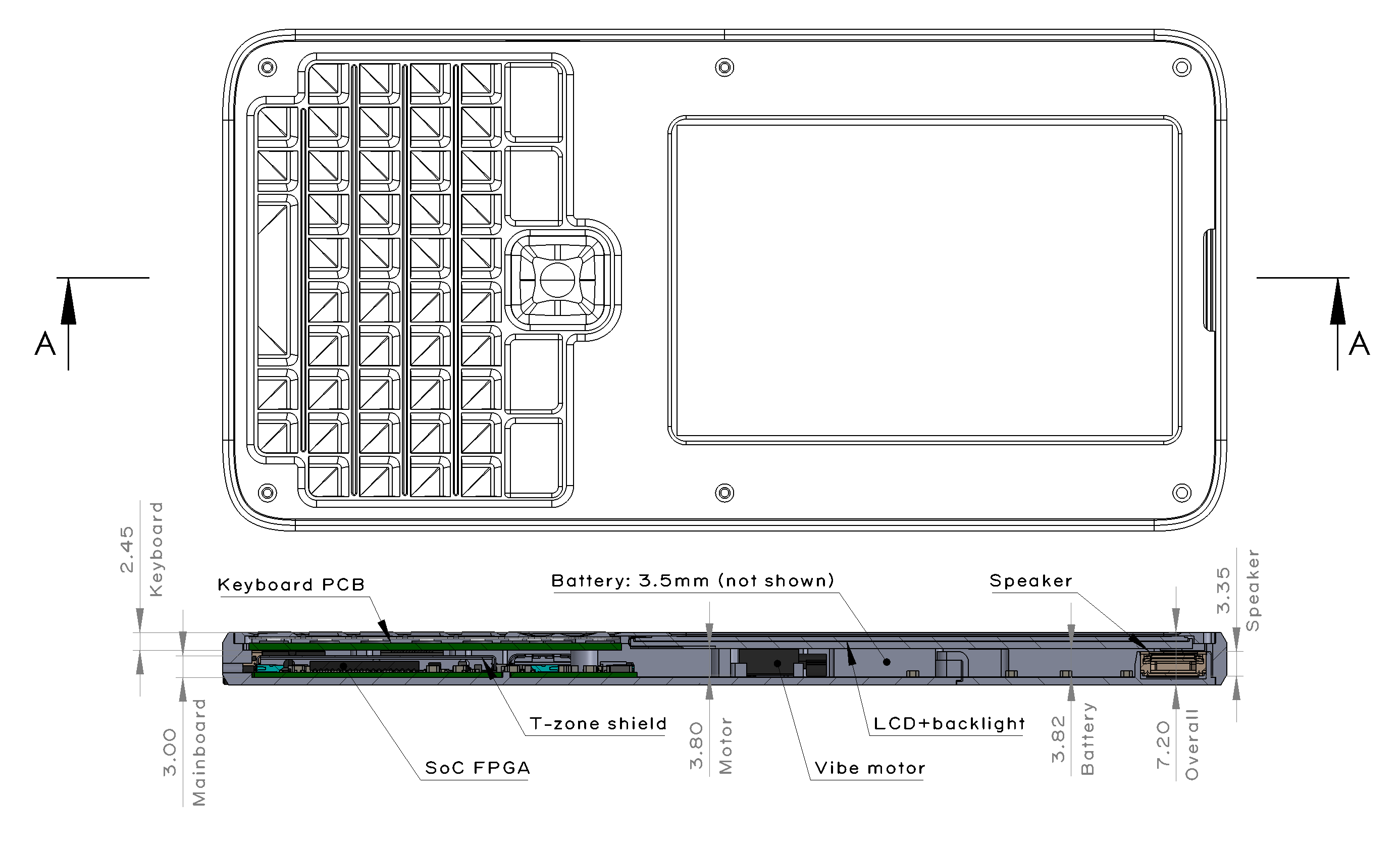
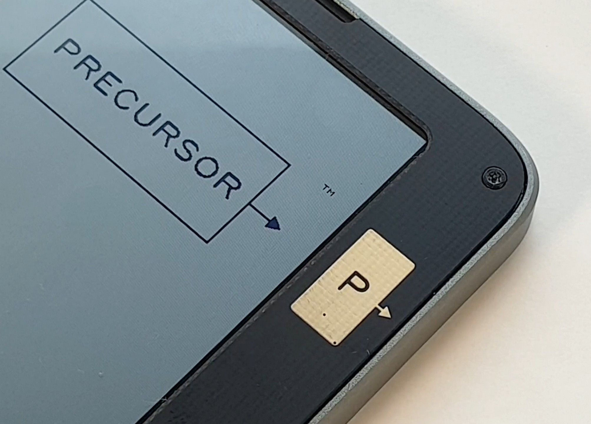
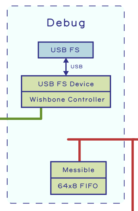
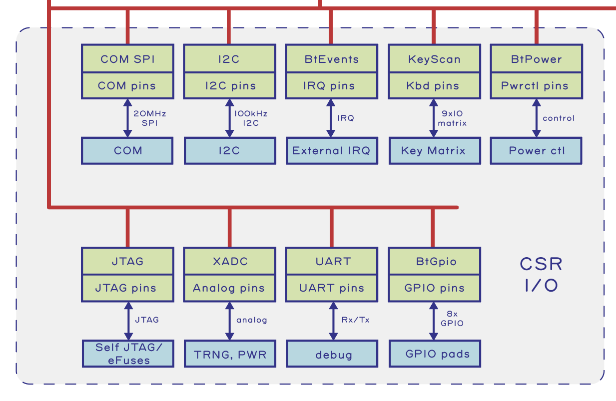
With Precursor, I’m bringing screws back.

Precursor’s screws are unapologetic – I make no attempt to hide them or cover them with bits of tape or rubber inserts. Instead, I’ve sourced custom-made Torx T3 metric screws with a black oxide finish that compliments the overall color scheme of Precursor. Six of them line the front, as a direct invitation for users to remove them and see what’s inside. I’ve already received ample criticism for the decision to show screws as “primitive”, “ugly”, “out of touch with modern trends” — but in the end, I feel the visual clutter of these six screws is a small price to pay for the gain in hackability.

Of course, the anti-screw critics question the value of hackability. Surely, I am sacrificing mass-market appeal to enable a fringe market; if hackability was so important, wouldn’t Apple and Google already have incorporated it into their phones? Wouldn’t we see more good examples of hackability already?

This line of questioning is circular: you can’t get good examples of hacks until you have made hackable products wide-spread. However, the critics are correct, in a way: in order to bootstrap an ecosystem, we’re going to need some good examples of why hackability matters.

In the run-up to crowdfunding Precursor, I was contemplating a good demo hack for Precursor. Fortuitously, a fellow named Matt Campbell opened a GitHub issue requesting a text-to-speech option for blind users. This led me to ask what might be helpful in terms of a physical keyboard design to assist blind people. You can read the thread for yourself, but I’ll highlight that even the blind community itself is divided on whether or not there is such a thing as the “blind ghetto” — an epithet applied by some users who feel that blindness-specific products tend to lag behind modern smartphones, tablets, and laptops. However, given that most modern gadgets struggle to consider the needs of 10% of the population that’s left-handed, I’m readily sympathetic to the notion that gadgets make little to no concession to accommodate the even smaller number of blind users.

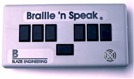
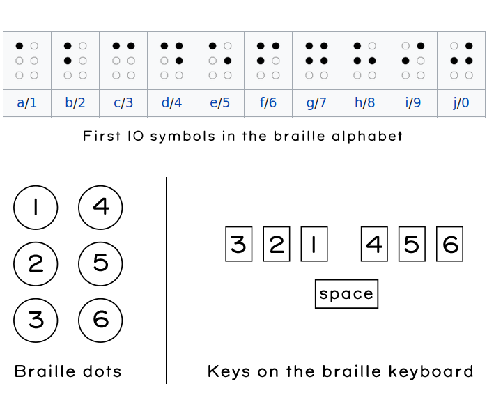
Matt was articulate in specifying his preferred design for a pocketable keyboard. He referred me to the “Braille ‘n Speak” (shown above) as an example of an existing braille keyboard. Basically, it takes the six dots that make up braille, and lines them up horizontally into three left and three right sets of buttons, adding a single button in the middle that functions as a space bar. Characters are entered by typing chords that correspond to the patterns of the six dots in the braille alphabet. Not being a braille user myself, I had to look up what the alphabet looked like. I made the guide below based on a snippet from Wikipedia to better understand how such a keyboard might be used.

Ironically, even though Matt had linked me to the picture of the Braille n’ Speak, it still took a while to sink in that a braille variant of Precursor did not need a display. I’m a bit ashamed to admit my first sketches involved trying to cram this set of switches into the existing keyboard area of the Precursor, without first removing the display entirely. I had to overcome my own prejudice about how the world should look and it took me time and empathy to understand this new perspective.

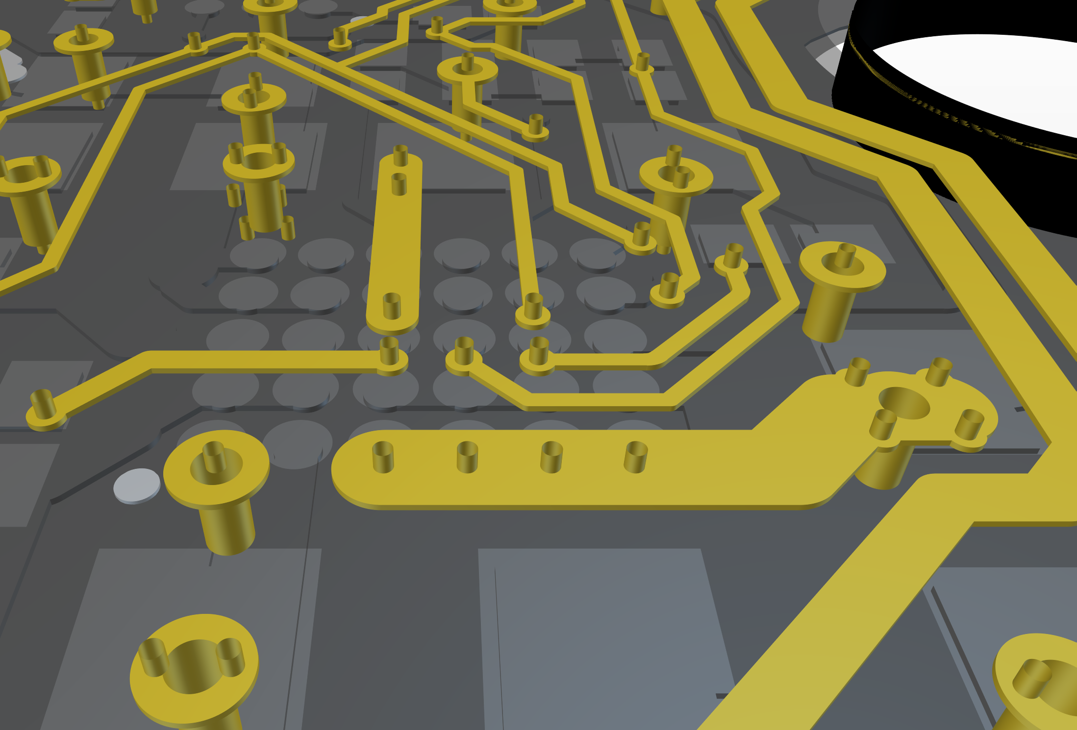
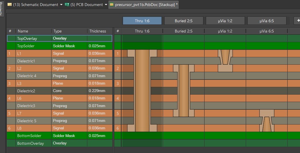
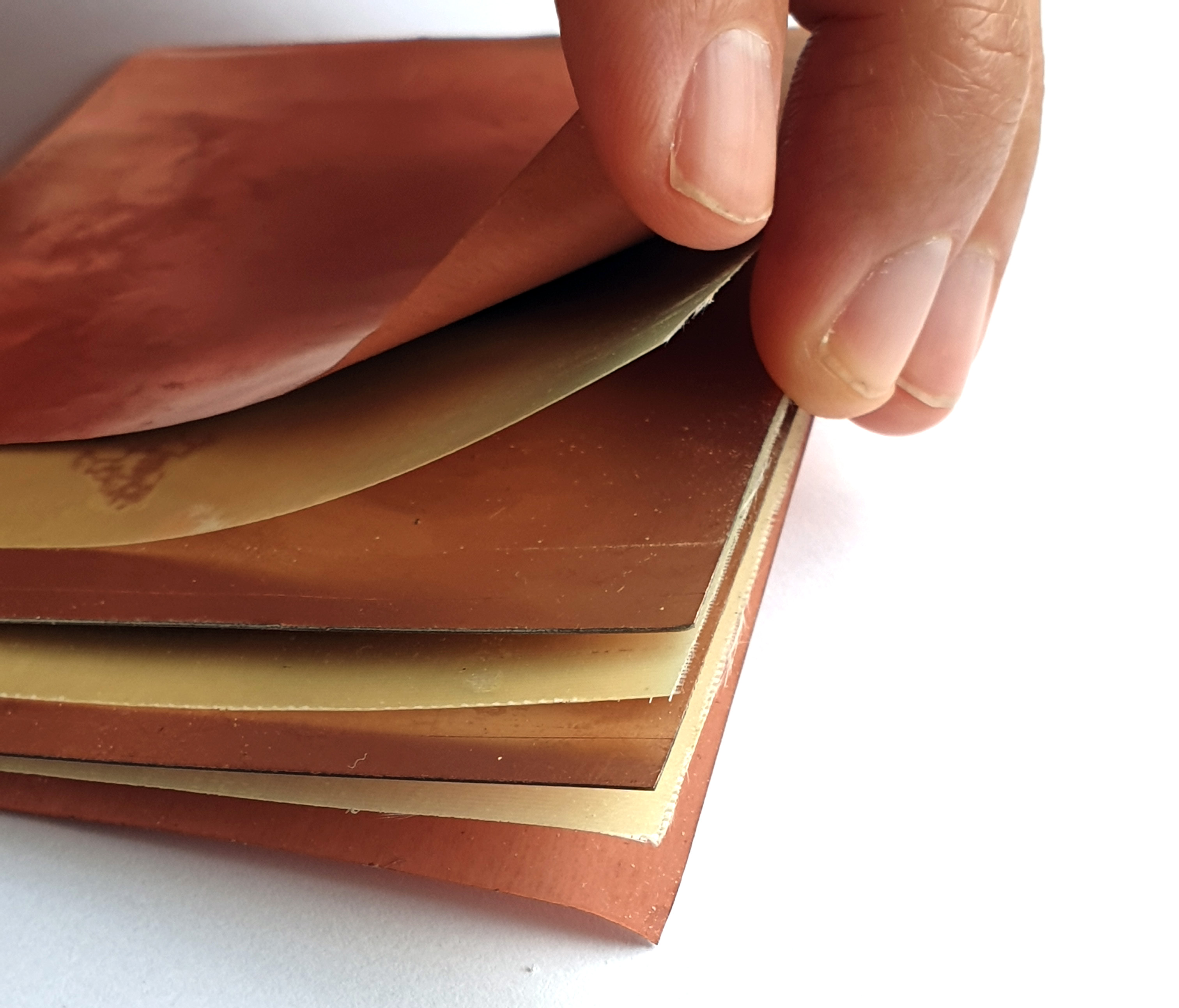
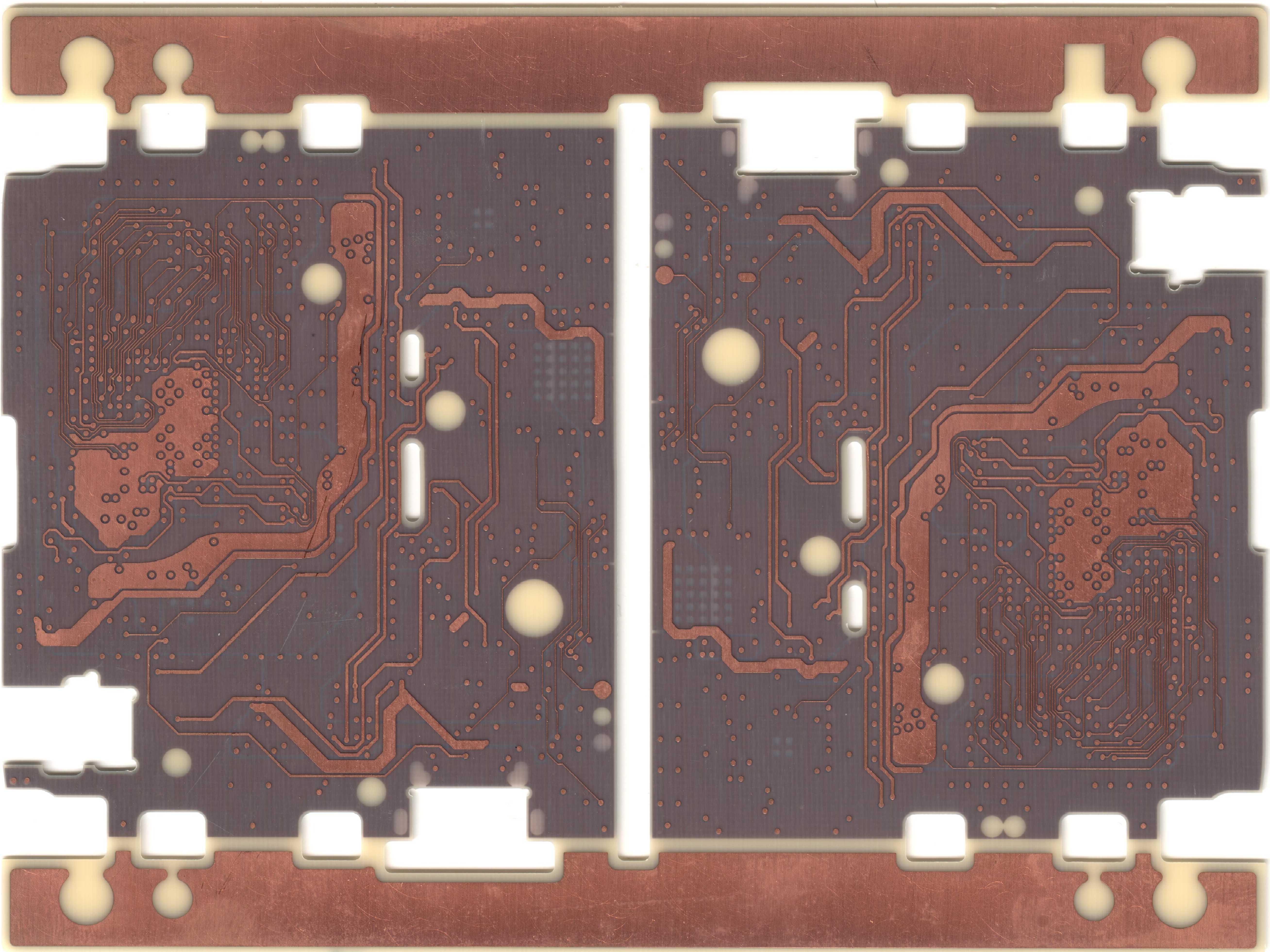
Once I had a better grasp of Matt’s request, I set about designing a customized braille variant. Precursor was designed for this style of hacking: the keyboard is a simple 2-layer PCB that’s cheap and easy to re-design, and the front bezel is also a PCB, which is a bit more expensive to redesign. Fortunately, I was able to amortize setup costs by bundling the braille front bezel variant with another variant that I had to fabricate anyways for the crowdfunding campaign. Beyond that, I also had to come up with some custom key caps to complement the switches.

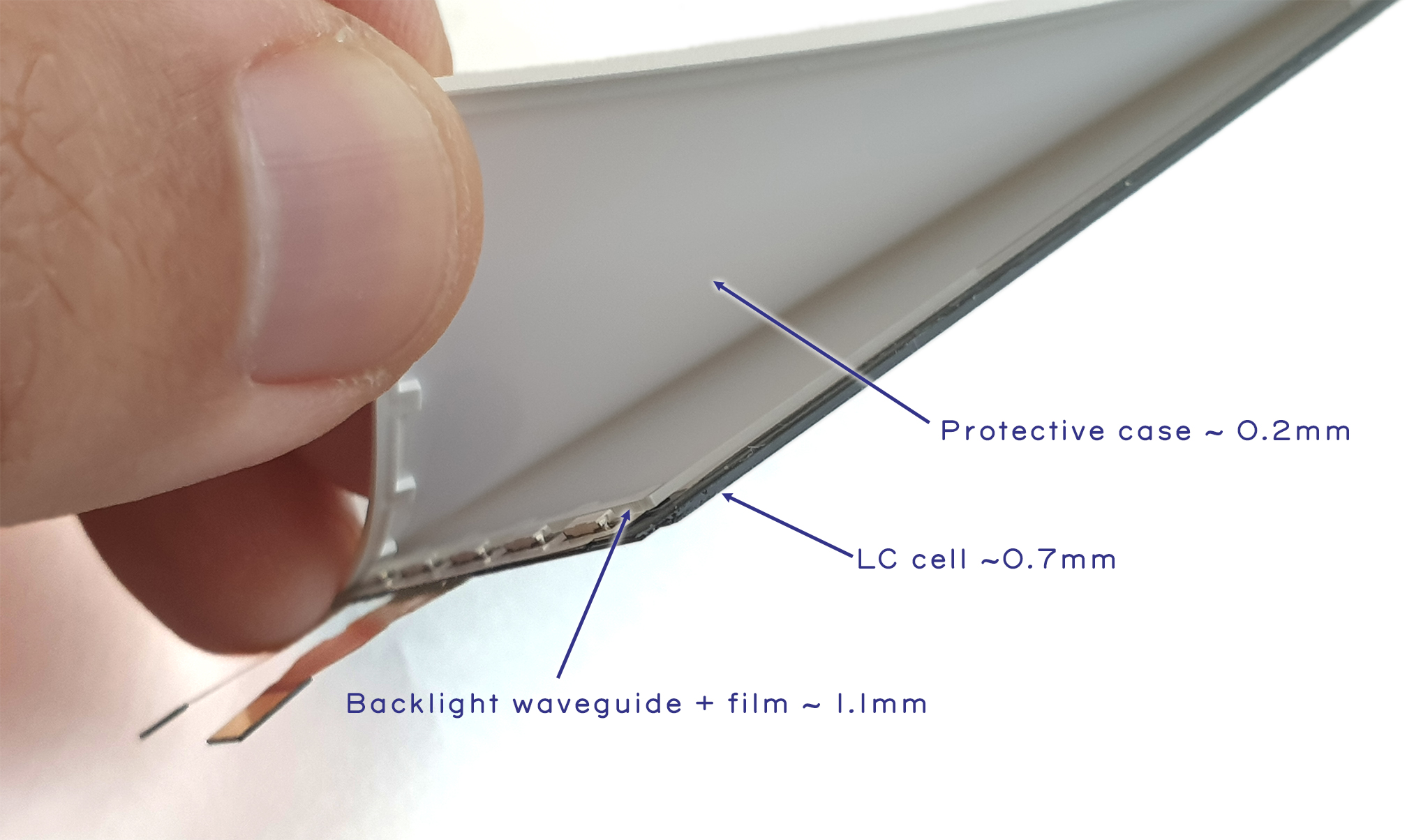
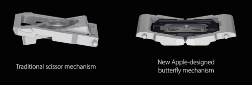
The major challenge in designing any type of mobile-friendly keyboard is always a trade-off between the hand feel of the switches, versus thinness of the overall design. On one side of the spectrum, full-travel mechanical switches have a wonderful hand feel, but are thicker than a sausage. On the other side of the spectrum, dome switches and printed carbon ink patterns are thinner than a credit card, but can feel mushy and have a limited “sweet spot” — the region of a key switch with optimal tactile feedback and operational force curves. The generally well-regarded Thinkpad keyboards go with a middle-ground solution that’s a few millimeters thick, using a “scissor” mechanism to stabilize the key caps over a silicone dome switch, giving individual keys a bit of travel while ensuring that the “sweet spot” covers the entire key cap. Optimizing key switch mechanisms is hard: some may recall the controversy over Apple’s re-design of the MacBook’s keyboard to use a “butterfly” mechanism, which shaved a couple mm of thickness, but led to lawsuits over a defect where the keyboard allegedly stopped working when small bits of dust or other particles got trapped under it.

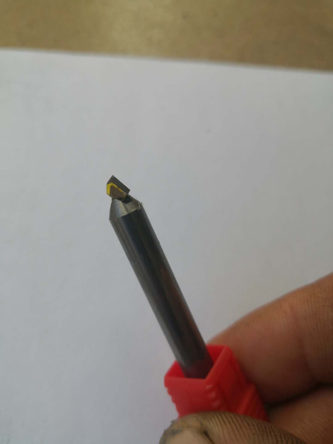
Given the short time frame and a shoestring budget, I decided to use an ultra-thin (0.35mm) tactile switch that I could buy off-the-shelf from Digikey and create custom key caps with small dimples to assist users in finding the relatively small sweet spots typical of such switches. I have sincere hopes this is a pretty good final solution; while it lacks a scissor mechanism to spread off-centered force, the simple mechanism meant I didn’t have to stick with a square key cap and could do something more comfortable and ergonomic to focus forces into the sweet spot. At the very least, the mechanism would be no worse than the current mechanism used in Precursor’s existing keyboard for sighted users, which is similarly a dome switch plus a hybrid-polymer key film.

Next, I had to figure out where to place the switches. To assist with this, I printed a 1:1 scale version of the Precursor case, dipped my fingertips in ink, and proceeded to tap on the printout in what felt like a natural fashion.

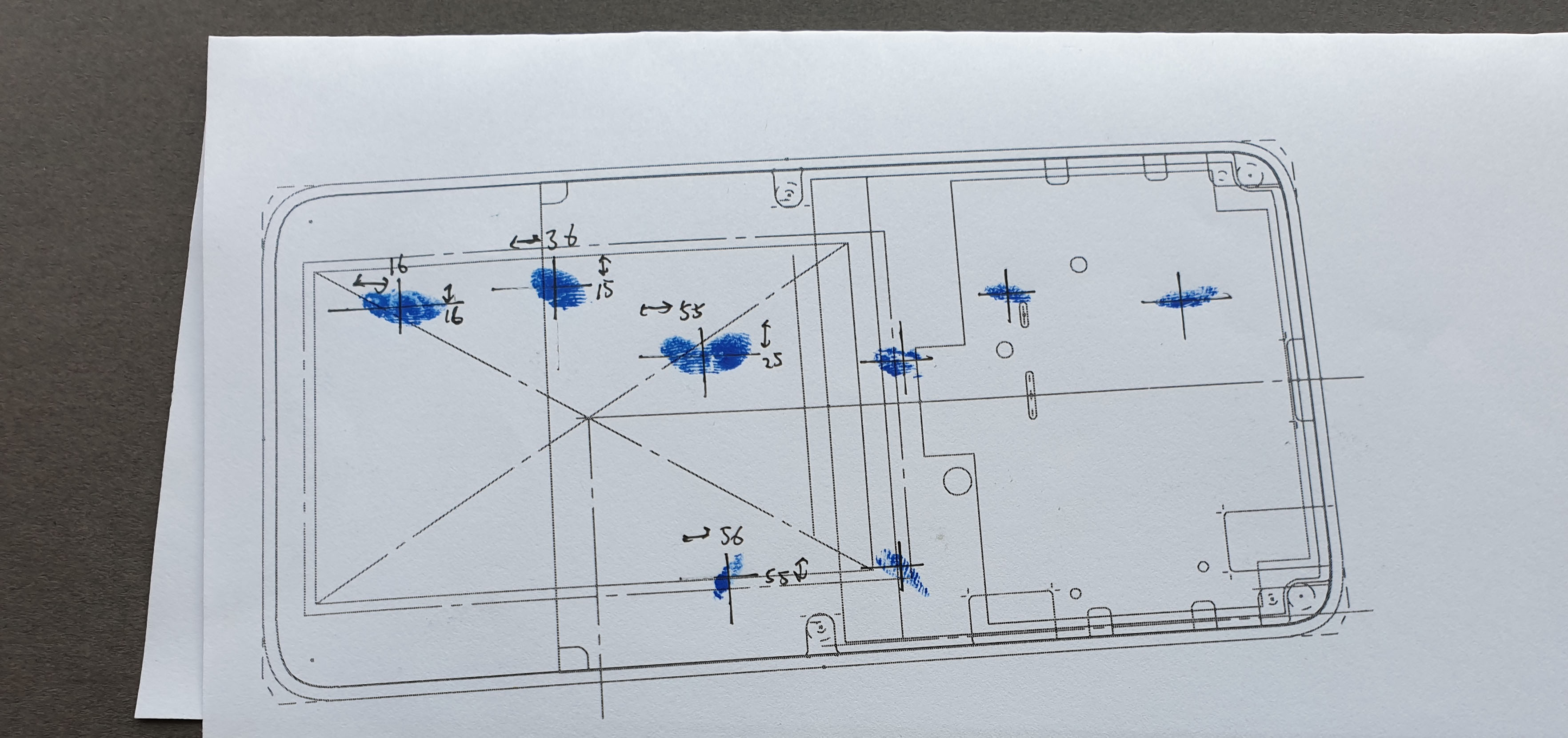
I then took the resulting ink spots and dimensioned their centers, to place the centroid of each key cap. I also asked my partner, who has smaller hands, to place her fingers over the spots and noted the differences in where her fingers lay to help shape the final key caps for different-sized hands.

Next, using the “master profile” discussed in the previous post on Precursor’s mechanical design, I translated this into a sketch to help create a set of key caps based on splines that matched the natural angle of fingers.

Above, you can see an early sketch of the key caps, showing the initial shape with dimples for centering the fingers.

Before moving ahead and spending a few hundred dollars to build a functional prototype, I decided to get Matt’s feedback on the design. We submitted the design to Shapeways and had a 3D print sent to Matt, which he graciously paid for. After receiving the plastic dummy, his feedback was that the center space bar should be a single key, instead of two separate keys, so I merged the two separate key caps of the space bar together into a single piece, while retaining two separate switches wired in parallel under the space bar. I felt this was a reasonable compromise that would allow for a “sweet spot” that serviced lefties as well as righties.

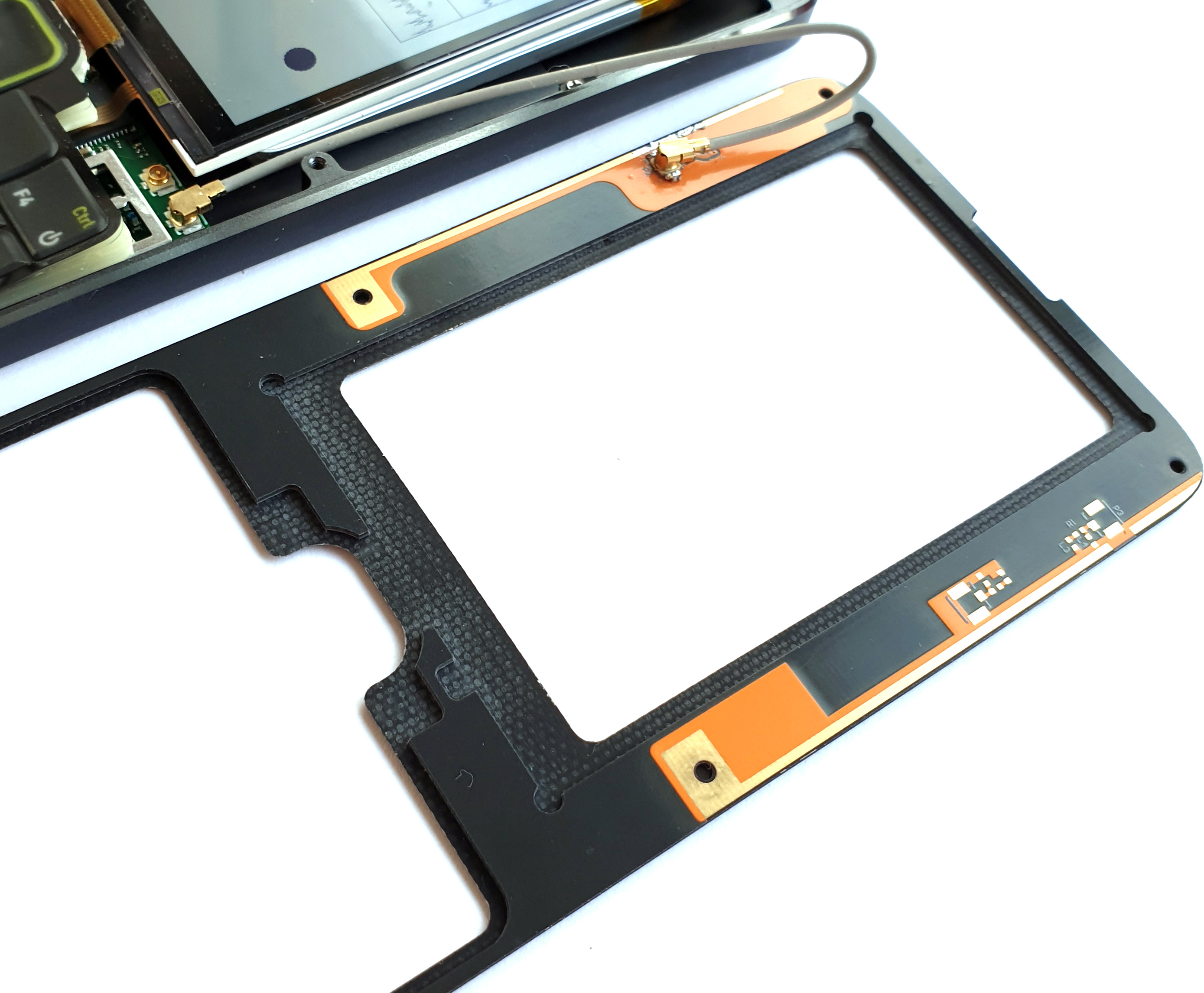
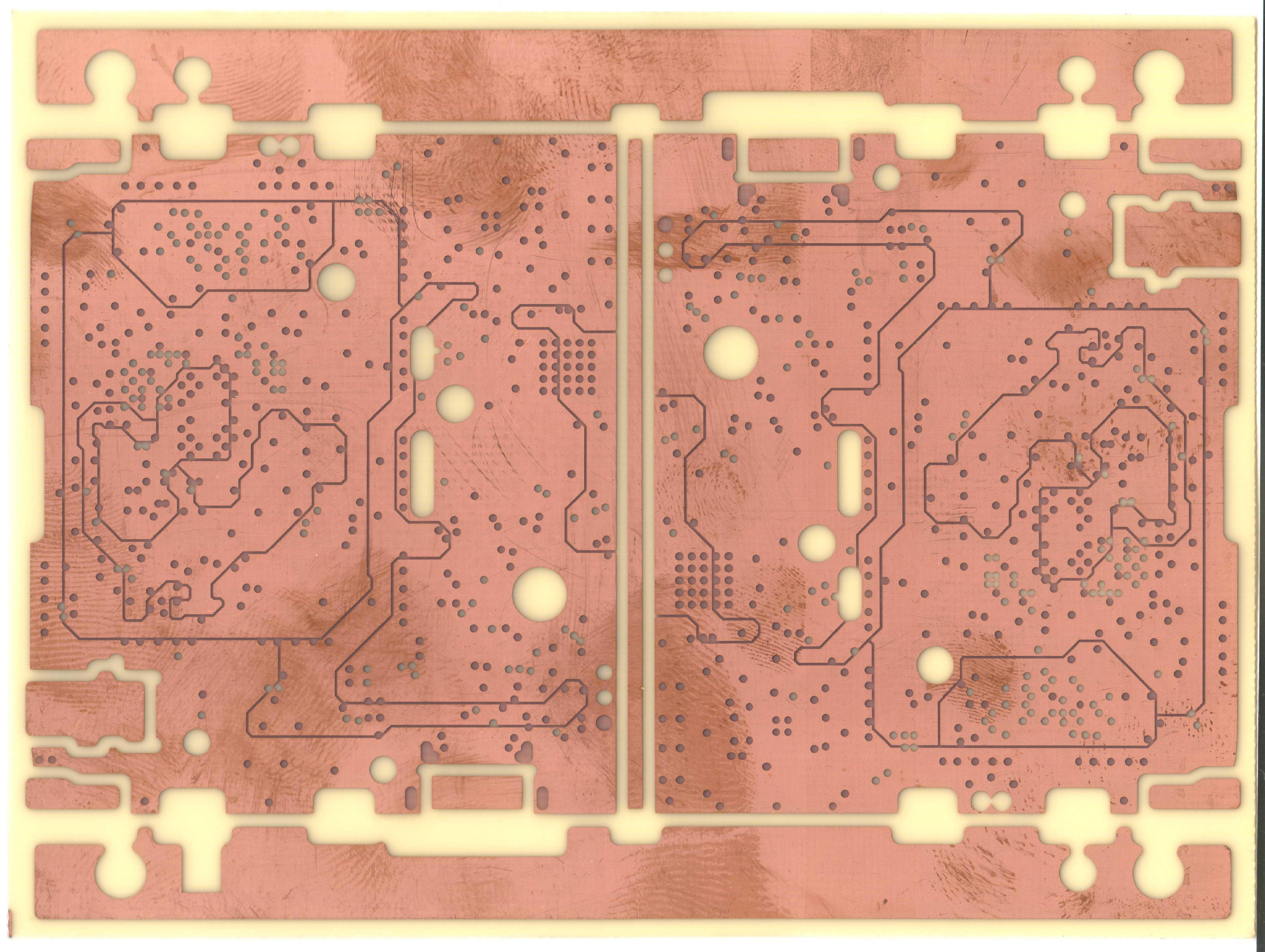
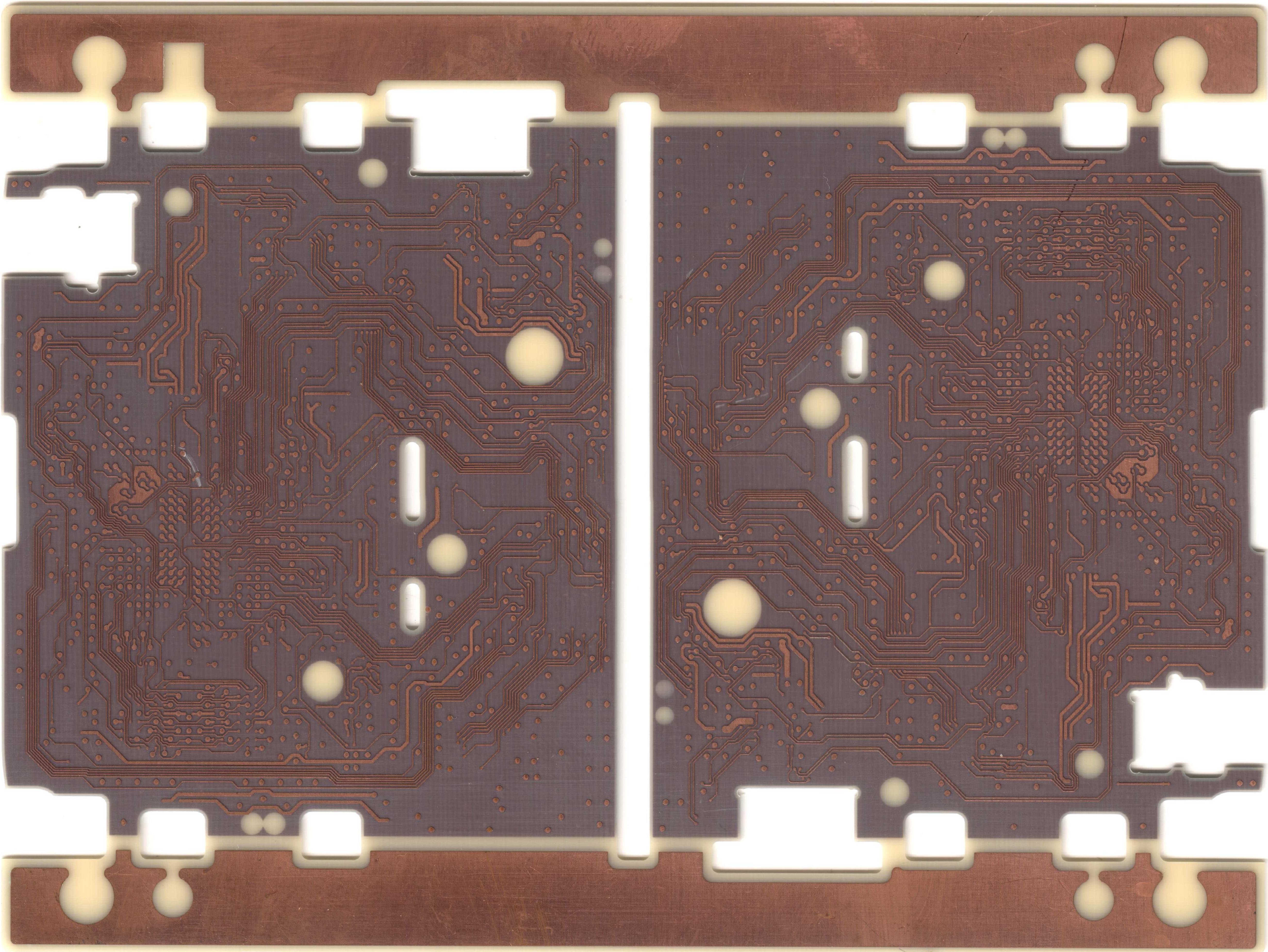
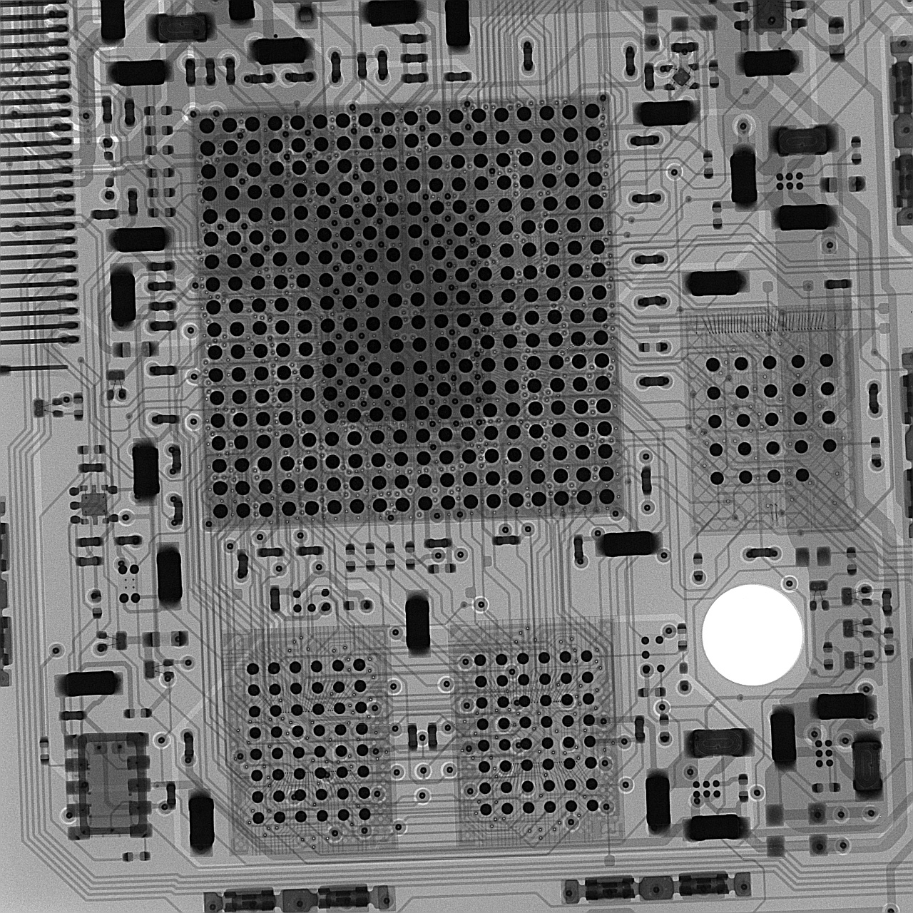
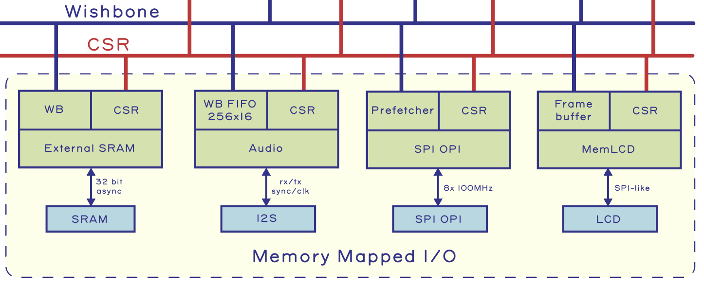
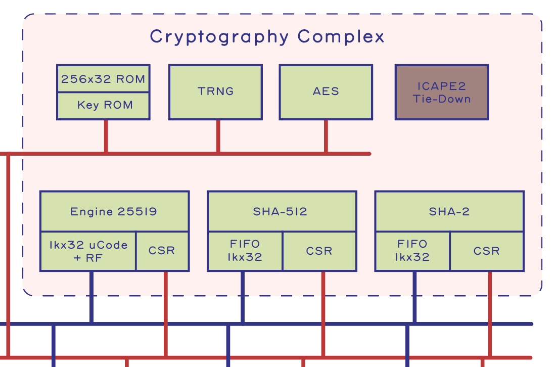
I then re-designed the keyboard PCB, which was a fairly simple task, because the braille keyboard consists of only eight switches. I just had to be careful to pick row/column pairs that would not conflict during chording and be sure to include the row/column pairs necessary to turn Precursor on after being put to sleep. I also redesigned the bezel; eliminating the display actually makes manufacturing a little bit easier because it also removes a beveling step in the manufacturing process. I kept the RF antenna in exactly the same location, as its design was already well-characterized and it takes a lot of effort to tune the antenna. Finally, I decided to manufacture the key switches out of aluminum. The switches have a lot of fine features and I needed a stiff material that could translate off-target force to the key switches to enlarge the sweet spot as much as possible.


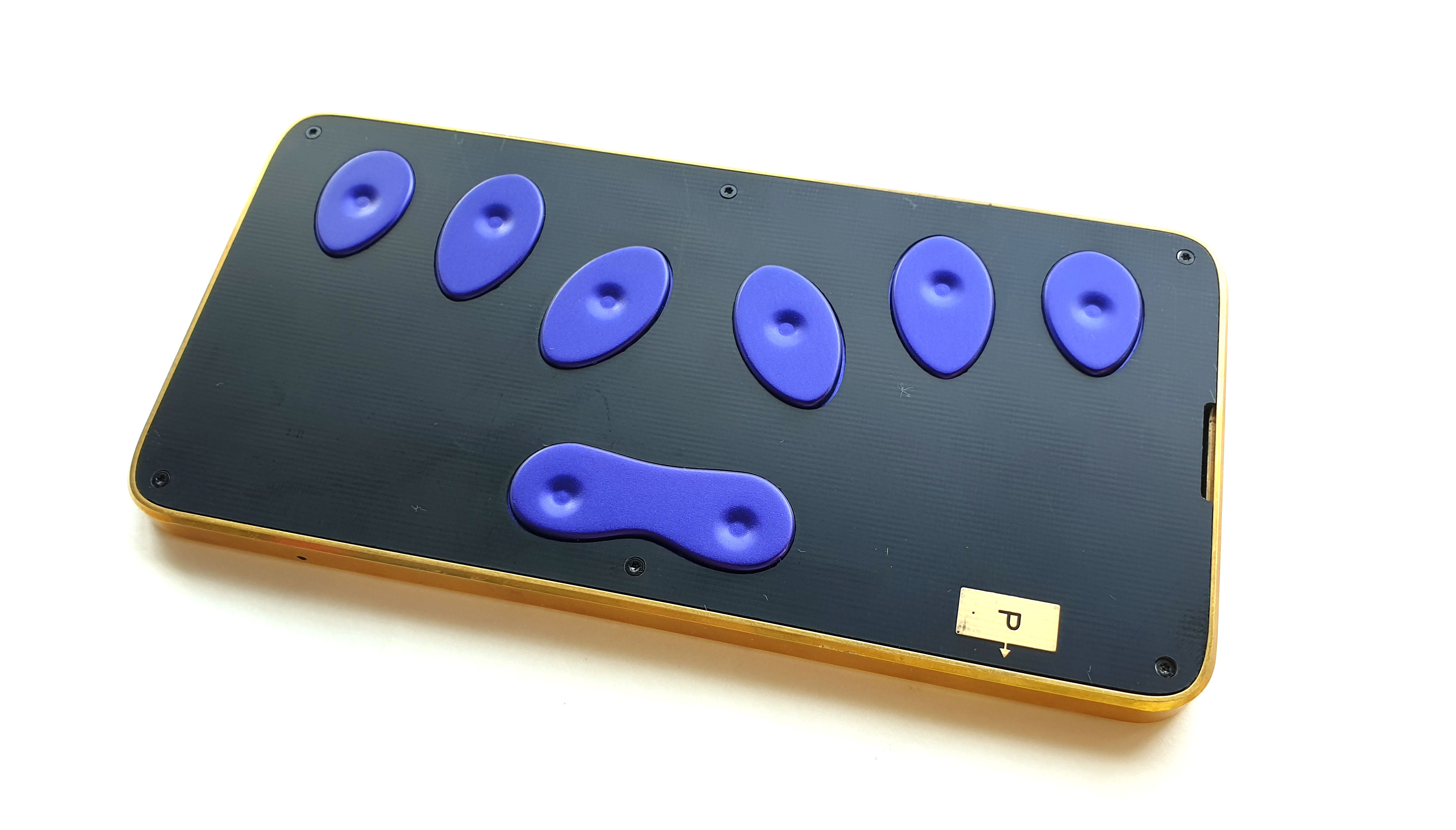
Above: The prototype of Precursor with braille keyboard.

About three weeks later, all the parts for the braille keyboard had arrived. I decided to use purple anodization for the key switches which, combined with the organic key shapes, gives the final design a bit of a Wakanda-esque “Black Panther” aesthetic, especially when mounted in a brass case. The key switch feel is about in line with what I imagined, with the caveat that one of the switches feels a little less nice than the rest, but I think that’s due to a bad solder job on the switch itself. I haven’t had a chance to trace it down because…well, I’ve had to write a bunch of posts like this to fund Precursor. I have also been working with Xobs to refactor Xous in hopes of putting together enough code to send Matt a prototype he can evaluate without having to write gobs of embedded hardware driver code himself.

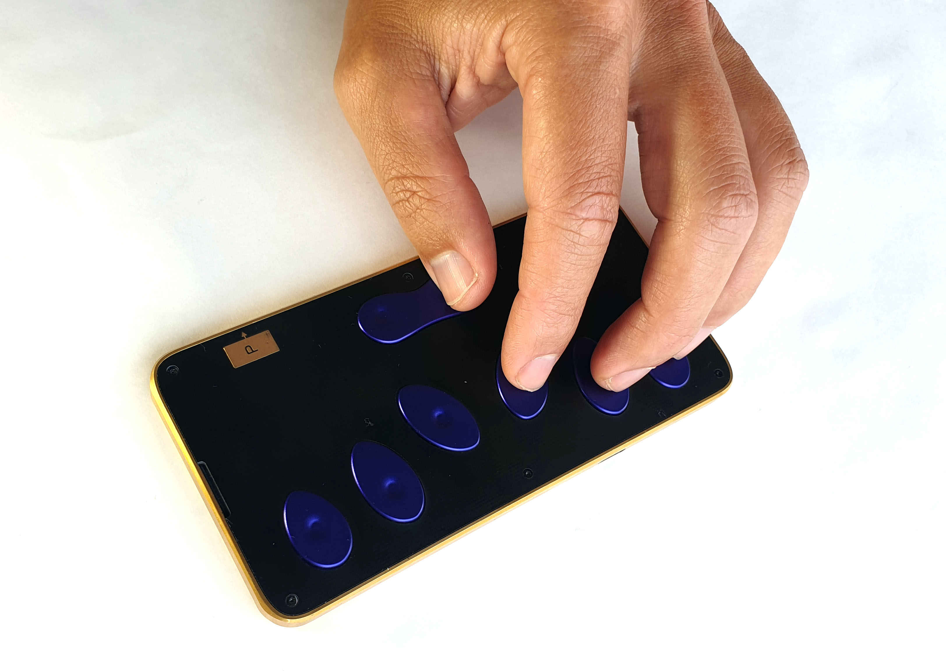
Above is a quick photo showing the alignment of fingers to keys. Naturally, it’s perfect for my hand because it was designed around it. I’m looking forward to hearing Matt’s opinion about the feel of the keys.

Above is a photo of the custom parts for the braille keyboard. At the top, you can see the custom bezel with key caps and the RF antenna matching circuitry on the top right. On the bottom, you can see the custom keyboard PCB mounted onto a Precursor motherboard. The keyboard PCB is mostly blank and, because of the small number of keys and the flexibility of the FPGA, there’s an option to mount more peripherals on the PCB.

Despite not being yet finalized, I hope this exercise is sufficient to demonstrate the potential value of hackable products. The original design scope for Precursor (née Betrusted) did not explicitly include a braille keyboard option, but thanks to modular design principles and the use of accessible construction materials, I was able to produce a prototype in about a month that has a similar fit and finish as the mainstream product.

As long as humans choose to embrace diversity, I think hackability will have value. A notional “perfect” product implies there’s such a thing as a “perfect” user. However, in reality, even the simple conundrum of left- or right-handedness challenges the existence of a singular “perfect” product for all of humanity. Fortunately, accommodating the wonderfully diverse, quirky, and interesting range of humanity implicates just a few simple engineering principles, such as embracing screws over adhesives, openness, and modularity. That we can’t hack our products isn’t a limitation of physics and engineering. Precursor demonstrates one can build something simultaneously secure and hackable, while being compact and pocketable. This suggests the relative lack of hackable products on the market isn’t a fundamental limitation. Maybe we just need a little more imagination, maybe we need to be a little more open-minded about aesthetics, and maybe companies need to be willing to take brave steps toward openness and inclusivity.

For Apple, true “courage to move on and do something new that betters all of us” was to remove the headphone jack, which resulted in locking users deeper into a walled-garden ecosystem. For hackers like myself, our “courage” is facing blunt criticisms for making “ugly” products with screws in order to facilitate mods, such as braille keyboards, in order to expand the definition of “all of us” beyond a set of privileged, “perfect” users.

I hope this braille keyboard is just the first example of many mods for Precursor that adapt the product for unique end-users, bucking the trend of gaslighting users to mold their behavior and preferences to fit the product. If you’ve got an itch to develop your own yet-to-be-seen feature in a mobile device, please visit our crowdfunding campaign page to learn more about Precursor. We’re close to being funded, but we’ve only a few days left in the campaign. After the campaign concludes on December 15th, the limited edition will no longer be available, and pricing of the standard model goes up. If you like what you see, please consider helping us to bring Precursor to life!

Precursor’s Mechanical Design

Monday, December 7th, 2020

“Pocketability” is the difference between Precursor and naked PCB FPGA development platforms. We hope Precursor’s pocketability helps bring more open hardware out of the lab and into everyday use. Thus, the mechanical design of Precursor is of similar importance to its electrical, software, and security design.

We always envisioned Precursor as a device that complements a smartphone. In fact, some of the earliest sketches had Precursor (then called Betrusted) designed into a smartphone’s protective case. In this arrangement, Precursor would tether to the phone via WiFi and the always-on LCD for Precursor could then be used to display static data, such as a shopping list or a QR code for a boarding pass, giving Precursor a bit of extra utility as a second screen that’s physically attached to your phone. However, there are too many types of smartphones out there to make “Precursor as a phone case” practical, so we realized it would make more sense to make Precursor a “stand-alone device”.

As such, we wanted Precursor to be unobtrusive and thin in order to lighten the burden of carrying a secondary security device. Our first-draft EVT design had Precursor at just 5.7 mm thick, placing it among the ranks of the thinnest phones. Unfortunately, the EVT device had no backlight on the LCD, which made it unusable in low-light conditions. Increasing the final thickness to 7.2 mm allowed us to introduce a backlight, while still being slimmer than every iPhone since the iPhone 8.

To minimize the thickness of Precursor, I first divided the design into major zones, such as the main electronics area, the battery compartment, the vibration motor, and the speaker. I then estimated the overall thickness of components in each zone and optimized the thickest one by either re-arranging components or making component substitutions until another zone dominated the overall thickness.


A cross-section view of the final Precursor design, calling out the dimensions of the various vertical height zones of the design.

After considering about a dozen or so mechanical layout scenarios, we arrived at the design shown above. Like every modern mobile device, when viewed by size and weight, Precursor is basically a battery attached to a display.

The practical limit on battery thickness is driven by the overhead of the protective wrapping around the battery. Lithium-polymer “pouch” batteries rapidly decline in energy density with decreasing thickness as the protective wrapper around the battery starts to factor appreciably into its overall thickness. The loss of energy density becomes appreciable below 3.5mm, and so this fixed the battery’s thickness at 3.5mm, plus about 0.2mm allowance for any swelling that might happen plus adhesive films.


Teardown view of Precursor’s LCD with backlight attached. Note that to inspect the transistors inside the LCD, the backlight module needs to be removed.

Display thickness is limited by the thickness of the liquid crystal (LC) “cell”, plus backlight. Fortunately, LC cells are extremely thin, as they are basically just the glass sheets used to confine a microscopic layer of liquid crystal material, plus some polarizer films – in Precursor’s case, the LC cell is just 0.705mm thick. The backlight is substantially thicker, as it requires a waveguide plus a film stack that consists of two brightness enhancing films, a diffuser sheet, adhesives, and its own protective case to hold the assembly together, leading to a net thickness increase of roughly 1.3mm. The backlight itself is actually a full-custom assembly that we designed just for Precursor; it’s not available as an off-the-shelf part.

With the display and battery thicknesses defined, the final thickness of the product is determined by the material selection of the protective case. We use aluminum for the bottom case and FR-4 for the bezel (we discuss the bezel in a previous post).

Using aluminum for the bottom case allows us to shave about 1 mm (~15%) of thickness relative to using a polymer like ABS or PC at the expense of a fairly substantial increase in per-unit manufacturing costs. Although polymers are about twice the cost of aluminum by weight, an aluminum case costs about 10x as much to produce. This is because polymers can be molded in a matter of seconds, with very little waste material, whereas aluminum must be CNC’d out of a slab in a time-consuming process that scraps 80% of the original material. Surprisingly, the 10x cost-up isn’t the waste material; there is an efficient market for buying and recycling post-machining aluminum. Most of the extra cost is due to the labor required to machine the case which is orders of magnitude longer than the time required for injection molding.

Thus, while we could have made Precursor cheaper, we felt it would both be more pocketable, as well as more desirable, with the machined aluminum case: it would look more like a high-end mobile device, instead of a cheap plastic toy or remote control.

Using aluminum also allows us to play some fun tricks with the fit and finish of the product, thanks in part to the transformative effect Apple had on the mobile phone industry. Their adoption of CNC machining as a mass production process sparked a huge investment in CNC capability, making once-exotic processes more affordable for everyone. A good example of this is the single-crystal diamond cutting process for making shiny beveled edges. This used to be a fairly expensive specialty process, which you can read more about in this great thesis on “Precision and Techniques for Designing Precision Machines” by Layton Carter Hale which, on page 27, describes the Large Optics Diamond Turning Machine (LODTM). The LODTM relies on the raw precision achievable with a diamond bit to create geometries for mirrors without the need for post-polishing.


A single-crystal diamond bit, courtesy of Victor from Jiada

I first learned about this technique in 2017, when I brought a Xiaomi aluminum mouse pad with a mirror-finish bevel.


Bevel on the Xiaomi mousepad

Despite a sub-$20 price tag, the mirror-finish bevel gave it quite an expensive look. Polishing to a mirror finish is a time consuming task, so I became curious about how this could be economical on a humble mouse pad. I bought another mouse pad, and brought it to Prof. Nadya Peek, and asked her how she thought it was fabricated. Readers who are familiar with our Novena laptop may recall her name as the designer of the Peek Array for mounting accessories inside the Novena. I’ve been lucky to have her mentorship and advice on all things mechanical engineering for many years now. So many of my products are better thanks to her!

She took one look at the bevel and immediately guessed it was cut by a single-crystal diamond bit, but she could do even better than making a guess. At the time, she was still a graduate student at the MIT Center for Bits and Atoms, where she had a Hitachi FlexSEM 1000 II equipped with the X-ray composition analysis option at her disposal. So, she took the mouse pad to the machine shop, chopped a corner off with a band saw, and loaded it into the SEM.


Viewing the output of the composition analysis.

If you zoom into the screen on the right, you can see the X-ray composition analysis reveals an unusually high amount of carbon on the aluminum surface (~10% by weight). Unlike iron, carbon is not commonly used in alloying aluminum. In this case, the chief alloying element seems to be magnesium, implying that the mousepad is probably a 5000-series alloy (perhaps 5005 or 5050). Given this, it seemed reasonable to conclude that the carbon residue on the beveled surface is direct evidence of a diamond cutting bit.


The shiny beveled edge on Precursor is brought to you by a single-crystal diamond milling bit.

Armed with this knowledge, I was able to work with Victor, the owner of Jiada – the primary CNC provider for Precursor – to specify a diamond-bit beveling process that brings you the nice edge finish on the final Precursor product. I also count Victor as one of my many mechanical design mentors; he’s one of those practicing-engineer-as-CEO types who has applied his extensive knowledge of mechanical engineering to open his own CNC and injection molding business. He always seems up for the challenge of developing new and interesting fabrication processes. That’s why I’ve been working closely with Victor to develop the campaign-only omakase version of Precursor.

Because Precursor’s case is CNC, we’re not limited to aluminum as the base material. It’s primarily a matter of cost and yield to manufacture with other materials. We could, for example, machine the case out of titanium, but the difficulty of machining titanium means we would likely have to machine two or three cases to yield a single one that passes all of our quality standards. This, combined with the high cost of raw titanium, would have added about a thousand dollars on to the final price of the omakase Precursor and we felt that would be just too expensive. Thus, Victor and I are currently evaluating two material candidates: one is physical vapor deposition (PVD)-finished stainless steel, the other is naval brass. These material choices were heavily influenced by Prof. Peek’s opinions. (It’s a coincidence the recently launched iPhone 12 uses PVD stainless steel for its case, as we have been working on this project since well before the details of iPhone 12 were publicly known.)

While both the PVD steel and naval brass are much more expensive than aluminum, they have a terrific hand feel and excellent machinability. Aesthetically, the main difference between the two is the color: for the stainless steel PVD, we’d be going with a high-gloss, polished black look, and for the naval brass we’re considering a brushed finish. The naval brass is more distinctive, but the soft metal is easy to scratch; a highly polished brass surface starts to look much less nice after a week or two of banging around in your pocket. A brushed finish hides such scratches and fingerprints better and over the course of years it should develop a handsome patina.

The major downside of the naval brass is that it’s highly conductive. Both the PVD stainless steel and anodized aluminum inherently have a tough, non-conductive surface layer; the naval brass does not. This is particularly concerning because if any of the internal battery connections get frayed, it could lead to a fire hazard. I’m currently working to see if I can find a surface coating that adequately protects the inside of the naval brass case from short circuits, but if I can’t find one, that may definitively rule out the naval brass option, leaving us with a PVD stainless steel case for the omakase version.

While good looks and a nice hand feel are significant benefits of going with a CNC process, another important reason I picked CNC over injection molding is anyone could build a full-custom version of a Precursor case in single quantities, with no compromise on finish quality or durability. Unlike the situation of injection molding versus 3D printing, which either use radically different base materials (for SLA 3D printing) or processes (for FDM 3D printing), your custom case can be made in single quantities with the exact same metal alloys and the exact same processes used in production Precursors.

This trait is particularly important for a mobile device and not just because the design works better when it’s built using its originally intended material system. It’s also because mobile devices don’t have a lot of extra space to devote to expansion headers and breakout boards. While it is beyond the level of a weekender hobby project to make a custom case, it’s probably within the scope of an undergraduate-level research project to undertake the necessary revisions to, for example, thicken the case and incorporate a novel medical sensor or a new kind of radio. In order to facilitate easier modifications to the case’s native Solidworks design file, I use a “master profile” to define the case body, bezel, and “ribbon” (the outer band that defines the height of the case). Helena Wang, another friend to whom I turn to for advice on mechanical design, taught me about the general technique of top-down modeling and using master profiles. Top-down modeling pushes a lot of design work into the up-front structure and planning of the 3D body in exchange for being able to revise the model without having to resolve dozens of conflicting downstream mechanical constraints. For example, when I realized I had to modify the case to be 1.5mm thicker to accommodate the backlight for the LCD, I was able to make the necessary change by just adjusting a single dimension in the ribbon height master profile, followed up by perhaps a half hour of cleaning up the offsets on structures which were defined outside of the master profile, such as the mounting points used to support the keyboard and the polymer radome that allows the WiFi signal out from the metal case.


A screenshot of the CAD tool view of the Precursor case, highlighting the master profile that defines the outer dimensions of the case.

Of course, making edits to the master profile requires access to a copy of Solidworks, which is not an open source tool; but FreeCAD users are welcome to redraw the design in their native format! I’ve heard good things about FreeCAD, but I just haven’t had the time to learn a new design tool. For smaller modifications that don’t involve changing major dimensions of the case – such as adding some extra through-holes for sensors or internal mounts for additional circuit boards – the case design is also available in a tool-neutral STEP format. Every CAD tool I know of can accept STEP format and, since it is actually the format used for CNC fabrication, it’s by definition sufficient for creating copies of the case.

If you’ve read my posts over the years, you may have noticed that I’ve never taken a formal course on mechanical engineering. Everything I know has been either gleaned from taking things apart, touring factories, scouring the Internet, and perhaps most importantly receiving advice from friends and mentors like Nadya, Victor, and Helena. It’s been a wonderful journey learning how things are made, I hope posts like this and the associated design files will aid anyone who wants to learn about mechanical design, so they may have an easier time of it than I did. Most of all, I’m hoping applying my experience and making Precursor pocketable and hackable will enable more open source technology to make it out of the lab and into everyday use, without requiring anyone to learn about mechanical design.

Thanks again to all our backers for bringing us closer to our funding goal! At the time of posting, we’re just at 90% funded, but we’re also getting down to the last week to wrap things up. We need your support to get us over the 100% mark. We recognize that these are difficult, trying times for everyone, but even small $10 donations inch us toward a successful campaign. Perhaps more importantly, if you know someone who might be interested in Precursor, we’d appreciate your help in spreading the word and letting them know about our campaign. With your help, hopefully we’ll blow past our funding goal before the campaign ends, and we can begin the hard but enjoyable work of building and delivering the first run of Precursor devices.

Precursor’s Custom PCBs

Tuesday, December 1st, 2020

While the last few updates about Precursor have focused on evidence-based trust and security, this update is more about the process of making Precursor itself. There is an essential link between evidence-based trust and understanding the manufacturing process: to convince yourself that something has been constructed correctly, it’s helpful to understand the construction process itself. It’s hard to tell if a small crack in a wall is the result of harmless foundation settling, or a harbinger of a building’s imminent collapse, without first understanding the function and construction of that wall.

Most designers like to abstract the PCB away as a commodity service, preferring “no-touch” or “one-click” ordering services where design files are uploaded and finished boards arrive in the mail, on time and at a good price. This is a bit like running a restaurant and ordering your produce from a mass distributor. The quality is uniform, delivery times are good, and the taste is acceptable. However, it’s hard to make a dish that’s really differentiated when basic ingredients all come from the same place.

I personally enjoy building electronics with a bit more of an artisanal flavor. Just as gourmet chefs invest the effort to develop relationships with their farmers, I’ve developed a personal relationship with my preferred PCB shop, King Credie. Since a PCB is at the core of virtually everything I build, I have found developing a healthy personal relationship with my PCB supplier has the benefit of raising the bar on virtually all my products. While King Credie is neither the cheapest nor the quickest-turn of PCB shops, their quality is consistent and, most importantly, they are willing to customize their process. For a small shop, they offer a wide variety of speciality processes, such as rigi-flex, metal core, edge plated cavities, HDI, and custom soldermask colors.

The Precursor Bezel

The bezel for Precursor, shown below, is a good example of how this flexibility can be used in practice. The front surface of Precursor is actually a raw FR-4 PCB while the Precursor logo is a 2.4GHz antenna. The two small black dots in the logo beneath the “P” are the antenna feed and ground stub vias, respectively, for a “PIFA” (planar inverse F)-style antenna. The PCB itself has been countersunk, beveled, and step-milled so it can function simultaneously as a mechanical bezel, an RF antenna, and a circuit board for electrical components.

Above is an inside shot of the bezel displaying step-milling and electrical circuitry on the inside surface of the bezel PCB. The back side components are for antenna impedance matching circuitry, connector, and ESD protection. A shiny layer of clear soldermask is applied, and you can clearly see the glass weave that forms the structure of FR-4 in the step-milled areas where material is removed. This constrains the LCD’s location and makes space for cables and keyboard components.

Example of a milling machine at King Credie (image courtesy Chris ‘Akiba’ Wong).

Although step-milling and countersinking are not considered “standard” processes for PCB manufacture, it turns out that all PCBs go through a milling (or routing) process anyways. This process defines their final shape by cutting them out of a larger mother panel. Above is a photo of such a machine doing edge routing. Here, the PCB panels are stacked about five or six panels high and a routing bit is defining the final outline of each of the smaller PCBs. Since the PCB shop already has several types of precision CNC machines that can do both routing and milling, getting countersinks and step-milling done is mostly a matter of buying the correct bits and convincing the shop to do it.

That last point is tricky: since most PCB shops compete solely on price, any disruptions in tooling can lead to costly mistakes. For example, if a machine was configured for countersinking but then the operator forgot to reconfigure it for routing, the machine might have the wrong bit installed for the next operator, and a whole panel would be lost at the final stage of production! Thus the risk of small process tweaks can be amplified by ripple-effects onto other volume processes.

Fortunately, King Credie has a pricing model where they largely separate the cost to set up a manufacturing run from the cost of production. Thus, for a highly bespoke PCB like this, I might pay a few hundred dollars to set up a production run, yet just a few bucks for the raw FR-4 material. The good news is that once the new process is finalized, the cost amortizes well over a production run the size of Precursor’s.

Of course, specifying such a bespoke processes is also a challenge. There isn’t a standard (that I’m aware of!) for communicating these types of things to a PCB shop, so I’ve mainly resorted to ad-hoc drawings on mechanical layers in my design tool.

Above is an example of how the bezel is specified to the manufacturer. Because of the complex 2.5D topology of this PCB, I also include several cross-sections to help clarify the drawings. I also try to make it so that the gerber lines are specifying either direct tooling paths or keep-outs (as opposed to using fills and polyregions and leaving it up to the shop to define a tool path within these regions).

Above: A King Credie engineer reviews and edits a customer’s design (image courtesy Jin Joo ‘Jinx’ Lee).

Of course, there’s a lot of email back-and-forth with the PCB shop to clarify things, and it takes an extra week to process the boards, But, it’s very important not to rush the shop when specifying highly bespoke designs because you want the best machine operators to run your boards, not just the ones who happen to be available that day. When things get really challenging, I know that King Credie’s CEO will personally go on the line to supervise production, but this is only possible because I let them prioritize correct results over fast turn delivery – he’s a busy guy, but it’s well worth the wait to get his personal assistance. He’s an engineer at heart and he knows the company’s capabilities like the back of his hand. And finally, it helps if I make it clear to the shop that for risky production runs like this, I will pay 100% of the quoted price, even if the scrap rate is high and they can only do a partial delivery. That being said, I’ve rarely been in a situation where the shop has had to adjust delivery quantities because of yield issues. I was lucky in that the bezel process worked on the first try (subsequent iterations were around refining the antenna shape and cosmetic details), but I’ve definitely had challenging PCBs where I’ve had to pay for two or three goes at process development before I had a process that worked right and yielded well.

The Precursor Mainboard

There’s another aspect of PCB manufacturing that is fairly ubiquitous yet surprisingly rare in the open source hardware world: microvias.

Above is a cross-section view of the Precursor PCB, lined up against a design view of the same. Here, the PCB has been cut through a ground pad for the wifi antenna, showing a stack of two laser-drilled microvias on top of a mechanically drilled via. As you can see from this image, two microvias can fit side-by-side in the area of a standard mechanically drilled via. To put it in solid numbers, the microvias here have a hole size of 0.1mm and an annulus of 0.2mm; and the mechanical via has a hole size of 0.25mm and an annulus of 0.5mm.

This style of via is absolutely essential in handheld products with space-conscious packaging featuring typical pitches of around 0.4mm for balls on a WLCSP.

Above is an example of one such WLCSP used on Precursor. The distance between each of the small round pads above is 0.4mm. You can see clearly here the contrast between the size of the mechanical drills and the laser-drilled microvias, and how essential they are for reaching the inner ranks of balls for these tiny packages.

Above is the same rough area of the PCB, but rendered in 3-D and highlighting the top layer only.

And above is the same area once again, rendered at the same angle but showing the second layer, underneath the top layer. These renderings help give an intuition for the relative scale and size of a microvia compared to a conventional mechanically drilled via.

I say that microvia technology is ubiquitous, because we all own at least one gadget that uses it liberally: our smartphone. Even the cheap $20 smartphones from the Shenzhen markets use microvia, so clearly it is a mature volume technology. However, very few open hardware products use it; to the best of my knowledge, Xobs’ Fomu was the first. My best guess as to its lack of popularity in open hardware is the high setup cost for microvia. But the high setup cost is driven in part due to a lack of demand and thus you have a classic chicken-and-egg problem blocking technological progress in open hardware.

As essential as microvia boards are for mobile gadgets, they are more expensive than through-drilled multi-layer boards for a few good reasons:

  • Laser drilled vias can only penetrate about 0.1mm thickness of material. Thus, they are almost always paired with a mechanical drilling process to get signals through the full thickness of a board.
  • Although drilling a single laser via is faster than drilling a mechanical via, a mechanical drill can penetrate several copies of the board at once, thus reducing the comparative speed benefit of laser drilling.
  • This combination of drilling processes means the board material has to be taken off the line several times for drilling operations, instead of being etched, laminated, and then drilled only once.
  • Stacked vias are almost always required with microvia designs and thus even the mechanical vias have to be filled in with copper to allow via stacking (normally they are left hollow in a regular multi-layer board).
  • Although mechanical drill bits must be replaced regularly, they can be recycled and reconditioned. Counter to my intuition, I was told that lasers (despite being solid-state) also wear out and require expensive periodic maintenance, particularly at the high power levels required for drilling.
  • Laser drilling is done with an X-Y CNC head, not with a galvanometer system as I had previously assumed, which significantly reduces the potential speed advantage of using light. Apparently this is related to the difficulty of keeping the laser focused over the entire dimension of the PCB and also the need to keep the drill hole vertical. I’m guessing there are probably more advanced laser drilling machines than the one I’ve seen which use a parabolic mirror with a single galvaonometer axis (similar to the Form 3).

Despite these extra costs, it’s virtually impossible to make a handheld gadget these days without microvia technology. The entire parts ecosystem for mobile devices assumes access to microvia technology, Without it, you just can’t access the latest technology in chargers, regulators, and other ICs.

Above is Precursor’s microvia “board layer stack” as seen in my design tool. It’s a 6-layer board. I have just two microvia layers (“top” uVia 1:2 and “bottom” uVia 6:5), paired with two types of mechanical drills, one which is a “buried” 2:5 layer and a “thru” 1:6. This type of layer stack is about the simplest microvia stack you can order (you could forgo the buried 2:5 layer, I suppose), but even this simple stack makes routing even the tightest 0.4mm BGAs in Precursor so easy, it almost feels like cheating.

In case you’re having trouble visualizing how this all comes together, I ordered a special run of Precursor boards from King Credie, where they pulled the material at each key process step so I could scan it and show you what the board looks like as it’s being made. (For the record, they did not sponsor this post – this post was my idea and I paid for all the extra PCB material that made it possible.)

All boards start as a uniformly copper-clad piece of FR-4 material, like the pieces shown above (image courtesy Akiba). Boards are built from the inside-out, so in the case of Precursor it starts with a piece of FR-4 that is about 0.23mm thick, with 0.018mm thick copper on either side.

The first step is to photo-image the inner layers, which in the case of Precursor are predominantly ground and power planes. The purple areas above are a thin layer of photoresist applied on top of a uniform copper foil layer.

Above: photo-imaging is done in a cleanroom with special lighting to avoid exposing the photoresist (image courtesy Akiba).

The photoresist protects the copper from being etched. The copper is chemically etched and the photoresist stripped, leaving just the etched copper pattern.

Above is the inner power layer of the Precursor PCB after etching and photoresist stripping. At this point, the PCB process is identical to that of a typical two-layer PCB.

After the inner layers are defined, the final “board stack” is created by laminating alternating layers of FR-4 and copper foil together.

Above is an example of a six-layer PCB stack (it’s not the exact one used in Precursor, but it illustrates the idea adequately). The yellowish material in between the copper layers is called FR-4, an epoxy-impregnated glass – basically, a type of fiberglass, the same kind of stuff used in Corvette car body panels and lightweight boats, which is why we can also use it as a structural material for the bezel of Precursor. The only difference for Precursor’s bezel is that a black dye is added to the base FR-4 material. A typical use for black FR-4 is in free-space IR technologies, such as remote controls, or front panels of equipment with LEDs inside, where the ability to fully block light across a wide spectrum can be important for functional reasons. But, in the Precursor bezel, we use the black color solely for aesthetics.

The “FR” designation stands for “flame retardant”. The PCB shop purchases it in two forms, one is called “core,” the other “prepreg”. Core FR-4 material is cured, so it is harder and stiffer; it’s basically the stuff inside your basic two-layer PCB. Prepreg is a “pre-impregnated” sheaf of glass fiber with epoxy. Since the epoxy has not been heat-cured, it’s substantially more flexible than core material, typically thinner, and can come with or without foil on one or either side. The prepreg is essentially a glue layer that is used to bind the copper layers together.

Once stacked together, the raw PCB material is put into an autoclave which heats the assembly to over 175C (~350F) while applying over 20x atmospheric pressure for about an hour. Above is an image of such an oven, where the hydraulic press racks are stored on the right, and the oven is in the center-left. During this process, the prepreg cures into its final, hardened form, flowing over the etched copper traces to fill all the voids.

Significantly, this pressing process reduces the overall thickness of the PCB. This is a very significant factor for applications that require impedance control or tight finished thickness control. Specifying buried impedance-controlled layers thus requires an additional step of analyzing the amount of pre-preg that flows into the voids between copper, because this affects the final distance to the adjacent ground planes and thus the final impedance. No board design software as far as I know accounts for this, because the physics of this flow depend heavily upon the specific precursor materials used. Thus, it’s important to send impedance-controlled PCBs to the PCB shop for analysis, so that final trace widths can be adjusted prior to tape-out for an accurate finished impedance.

In the case of Precursor, an extra layer of pre-preg + copper is added to either side of the two-layer core, creating a four-layer PCB structure as shown above. At this point, the coarse board outline routing structures are defined. This includes the gaps for processing rails, through-hole components, and mounting features. Alignment holes to assist with alignment for future process steps are also added in the material outside the finished panel. Although the structure above looks like a blank PCB, it in fact already holds the internal ground and power planes! This is an important fact to keep in mind when contemplating the potential for this process to hide implants within a PCB laminate stack.

The PCB then goes through a pass of mechanical drilling, plating, etching, and hole back-filling, ending up with the four-layer PCB structure shown below.

The above shows the top and bottom sides of the inner four-layer stack of Precursor. Mechanical through-holes have been drilled, but notice how they have been completely back-filled with copper so that there are no voids, allowing us to stack microvia on top of the mechanically drilled holes.

If we were making a conventional four-layer PCB, we’d be done at this point! But, because we’re doing microvia, the PCB has to make yet another pass through the PCB shop’s laminate-etch-drill process. Any yield defects after to this point start to get very expensive, so the PCB shop has to have its process control spot-on to build a microvia process.

The Precursor PCB gets yet another extra layer of prepreg + copper laminated on, so it once again looks like the “bare” PCB photo shown a bit above, then it’s sent into the laser drilling process.

After the laser drilling process, you can barely see the tiny 0.1mm holes pitting the surface of the copper, which is now dusty with a reddish-brown protective oxide layer naturally resulting from the lamination process. I believe the protective layer also assists with the adsorption of laser radiation for more efficient drilling, as bright shiny copper may be too reflective to light.

Above is an enlargement of the 0.1mm laser drill holes around the SRAM ball-out area of Precursor.

Next, Precursor’s PCB is put through a step where the precision through-holes for layer 1-6 vias as well as slots and mounting pads are added. This is all done with a mechanical drill with a diameter no smaller than 0.25mm.

Now that both the laser and mechanical holes are drilled, Precursor’s PCB goes through a special step where the laser drilled vias are electroplated and filled to form functional and flat via-in-pad structures. Via-in-pad flatness is important to avoid assembly problems with the tiny WLCSP parts. At this point, the reddish oxide has been stripped off with an acid wash (which reduces the finished thickness very slightly, less than a micron), and the copper is once again shiny (even though this image doesn’t emphasize the reflective highlights so the vias are a bit easier to see). Excess plating is milled off the edges of the larger board’s cut-out features (such as the large gaps between the board panels), but the plating is left in-place on the smaller holes, even the non-plated ones.

Above: an automated line used to plate copper onto PCBs.

Above: a view inside one of the many baths in the plating line.

Finally, Precursor’s PCB is taking a shape that we might recognize! Here, a “photoresist” layer has been added to define the outer traces. The astute observer will note the masked regions which are the regions of copper we want to *etch*, not the regions we want to *keep*. You’ll also note this “photoresist” is somehow able to cover large holes.

For the outer layers, it turns out that a “dry film” is used instead of an ink-like photoresist. One reason for this is we’re no longer dealing with a 2-D plane of copper: we have some plated-through holes we need to protect, and some non-plated holes we need to etch. A planar resist cannot adequately protect 3-D holes from etching. Thus, the board is covered with a conformal, photoreactive dry film capable of covering small holes. The dry film is exposed and developed to reveal the copper we wish to keep.

This brings us to the second reason for using the negative. At this point, additional copper is plated onto the unmasked copper regions to thicken the thin initial plating used to seed the mechanically drilled via holes, This simultaneously increases the finished thickness of the outer copper traces.

The masked and plated board is then dunked in a tin-plating bath that will fully cover all the exposed surfaces, including the 3-D structures of the plated-through vias we wish to keep. The tin plating can now serve as the etch mask. Next, the PCB is dunked into an etch vat to remove the photoresist and unwanted copper from not just the planar surfaces, but also from the vertical surfaces of the non-plated holes. Now etched, the PCB is finally stripped of the tin, leaving us once again with bare copper.

We’ve finally arrived at the near-finished six-layer, microvia PCB structure. At this point, all the electrically relevant structures have been built, so we just need to worry about the surface finishes.

A protective layer of green soldermask is applied over the PCB. The soldermask is a photosensitive ink that is exposed in a process very similar to the photoresist process. Therefore it can image the very fine structures necessary to surround the tiny 0.4mm-pitch BGA structures used in Precursor. Almost any color of soldermask can be used, but green is the most common. At this point, small gaps in the soldermask are also imaged to assist with aligning the future v-scoring step.

Next, a white silkscreen layer is applied. The silkscreen is mostly for human operators later in the process to know where components go. Normally, each component would have a “designator” attached to its location, but because we’re using predominantly 0201-sized components (a bit larger than a grain of salt), such designators would be illegible and not very useful. Instead, we pay a fairly hefty set-up fee for the SMT machine operator to go through a full manual check of the machine programming before assembly. Note that at this point, the pads are still bare copper and subject to oxidation if left exposed to air for a long time.

Above is the finished Precursor board, after the final two steps have been run: immersion gold plating and v-scoring. The immersion gold process deposits a very thin layer of gold over the exposed copper pads, protecting it from the elements. We use this instead of “HASL” (hot air levelled solder) because HASL is unable to achieve the planarity required for our small component geometries. “V-scoring” is the process of cutting V-shaped notches into the surface of a PCB to facilitate breaking off the sacrificial rails on the top and bottom (necessary for automated handling during the SMT process). You can see the subtle horizontal notches from the V-score in the image above.

Now finished, the board goes through an electrical test where every combination of pads is individually tested using a “flying probe” tester. These testers consist of several pairs of probes that can check the continuity of up to a hundred traces per second. On a complex board like Precursor’s, this test can take several minutes per board and is a significant driver of cost, After crowdfunding, some of the proceeds will be used to produce a “clamshell” type of test fixture with a bed-of-nails style tester to check all the circuit connections in a single mechanical operation.

After testing, the boards are packaged and sent to the SMT shop for assembly. And that’s how microvia PCBs are made! Precursor’s design would be classified as one of the simplest microvia constructions; smartphones will have 10 or more layers in their construction. Still, we can see why this construction is more expensive than on a conventional multi-layer board, since every successive microvia layer pair the PCB has to run through requires a full laminate, drill, and etch process cycle. Despite the extra cost, microvia is essential for mobile gadgets. As consumers demand ever-shrinking sizes, mechanically drilled vias can no longer meet routing density requirements. In addition to being a quarter the size of a mechanically drilled via, the use of blind through-vias in a typical microvia stack means component placing on the top and bottom side is largely independent of each other — it’s a bit like getting two PCBs in the space of one. This combination of denser vias and top/bottom placement freedom translates to a greater than 4x improvement in functional density over a conventional multi-layer board. In other words, even if we could make Precursor cheaper by using a conventional multi-layer board, it would be about 4x its current volume (about twice as thick, and perhaps 50% wider and longer)!

Finally, for the security-minded reader, there are a few observations we can make about implants in PCBs, now that we understand the detais of its construction. Because a PCB is made from a laminated stack of materials, we can see how it is possible to laminate an implant into a mid-layer of a PCB. The main trick is making sure the laminated implant can survive the autoclave conditions of 20x atmospheric pressure and 175C for an hour. It’s not inconceivable for a silicon chip to survive this, as they must survive soldering and package overmolding processes anyways.

If I were to do a buried implant in a PCB, I would build the inner core layer with the wirebonding pattern for the implant chip. Then I’d laminate the next layer of FR-4 with a cavity (an opening) for the implant chip, using a low-flow prepreg to bond the layers together. I’d then do a selective gold deposition on the chip’s bonding pads and wirebond the implant chip directly into the cavity. Note that chips are routinely thinned to less than 0.1mm in thickness, so the height of the chip is similar to that of the PCB laminate material. After bonding, I’d then encapsulate the implant chip in an epoxy (similar to the Epotek 301 resin shipped with Precursor for security sealing) to protect the wirebonds, then polish back any excess epoxy material so there is a smooth, void-free surface. At this point, I’d do a quick functional check of the implant before proceeding to the final FR-4 lamination steps, which would, as noted previously, obscure the implant’s presence from visual inspection.

I estimate such a process could be developed in a matter of months (assuming non-pandemic times when travel to the factory was possible) for a few thousand dollars of material and process cost, assuming the implant chips were already available in a pre-thinned, known good die form. Thus, I’d say it’s neither hard nor inconceivable that one could bury an implant in a PCB; you don’t need to be a spy agency with a billion dollar budget to pull it off. However, detection of the implant is also pretty easy, as the chip would readily show up in any X-ray scan. Alternatively, an IR imager would likely pick up its presence, as the region of the implant would have a differential thermal conductivity and the implant itself may give off heat. Finally, if the chip isn’t carefully placed between two contiguous power planes, it could be picked out by simply shining light through the board. Thus, while it’s on the easier end of implants to execute, it’s also on the easier end of implants to detect.

Above is an x-ray view of an assembled Precursor PCB. A buried implant in the PCB would show up quite readily in such a scan, as you would see both modifications to the design’s trace pattern as well as the implant’s bond wires quite clearly in an x-ray. Note that x-ray scans like this are routine for quality management purposes during the manufacture of high-end electronic products.

If you want to learn more about Precursor, check out our crowdfunding page. Pre-orders help ensure that we can amortize all the setup costs of building our microvia PCBs. Even if Precursor isn’t the gadget for you, if you enjoyed this article, please consider leaving a donation by participating in the “buy us a couple of beers!” pledge tier.

Evaluating Precursor’s Hardware Security

Monday, November 23rd, 2020

Making and breaking security go hand in hand. I’ve talked a lot about how Precursor, a mobile hardware development platform for secure applications, was made. In this post, I try to break it.

Hardware security is a multi-faceted problem. First, there is the question of “can I trust this piece of hardware was built correctly?”; specifically, are there implants and back doors buried in the hardware? We refer to this as the “supply chain problem”. It is a particularly challenging problem, given the global nature of our supply chains, with parts pulled from the four corners of the world, passing through hundreds of hands before reaching our doorstep. Precursor addresses this problem head-on with open, verifiable hardware: the keyboard, display, and motherboard are easy to access and visually inspect for correct construction. No factory or third-party tool is ever trusted with secret material. Precursor is capable of generating its own secret keys and sealing them within the hardware, without additional tools.

We also use a special kind of logic chip for the CPU – an FPGA – configured by the user, not the factory, to be exactly the CPU that the user specified. Crucially, most users have no evidence-based reason to trust that a CPU contains exactly what it claims to contain; few have the inspection capability to verify a chip in a non-destructive manner. On the other hand, with an FPGA, individual users can craft and inspect CPU bitstreams with readily available tools. Furthermore, the design can be modified and upgraded to incorporate countermeasures against hardware exploits discovered in the FPGA’s underlying fabric. In other words, the current trustability situation for an ASIC-style CPU is basically “I surrender”, whereas with an FPGA, users have the power to configure and patch their CPUs.


See my previous post for more details on how an FPGA helps solve the problem of transparency in CPU designs

Trustable hardware is only one facet of hardware security. Beyond correct construction, there are also questions of “has anyone tampered with the hardware while I wasn’t looking?”, and “can my hardware keep its secrets if it falls into the wrong hands?” These are the “tamper evidence” and “tamper resistance” problems, respectively. The rest of this post will drill down into these two questions as they relate to Precursor.

Despite any claims you may have heard otherwise, tamper resistance is a largely unsolved problem. Any secrets committed to a non-volatile format are vulnerable to recovery by a sufficiently advanced adversary. The availability of near-atomic level microscopy, along with sophisticated photon and phonon based probing techniques, means that a lab equipped with a few million dollars worth of top-notch gear and well-trained technicians has a good chance of recovering secret key material out of virtually any non-volatile storage media. The hard part is figuring out where the secrets are located on the chip. Once this is known for a given make and model, the attack is easy to repeat. This means the incremental cost of recovering keys from a previously studied design is in the ballpark of $10k’s and a matter of days. For some popular types of silicon packaging, such as flip chips, so-called “back side probing” techniques may be able to non-destructively extract secret key material within a matter of hours.


Ptychographic X-ray imaging as referenced in this article reveals the detailed 3-D structure of a modern chip.

Keys stored in volatile memory – that is, battery-backed RAM – can significantly up the ante because any disruption of power to the key memory can disrupt its data. Cryogenic freezing of the circuitry can help preserve the data for readout in the event of power loss, but battery-backed key storage can also incorporate active countermeasures to detect environmental anomalies and reactively zeroize the keys. While this sounds great for storing extremely sensitive secrets, it’s also extremely risky because false triggers can erase the keys, millions of dollars of cryptocurrency could vanish with a single false move. Thus volatile keys are best suited for securing highly sensitive but ephemeral communications and not for the long-term storage of high-value secrets.

Tamper evidence, not to be confused with tamper resistance, is the ability of a secured hardware device to show evidence of tampering. An example of very basic tamper evidence is the “warranty void if removed” sticker. It is typically placed over a screw essential to holding the case together, so that any attempt to disassemble the unit requires puncturing the sticker. This very basic measure is easily defeated by duplicating and replacing the sticker, and it’s not hard to acquire even the holographic stickers if you know the right people.

The next level up in tamper evidence is the incorporation of a physically unclonable feature in the tamper-evident seal, such as meauring the random pattern of fibers in the paper of the sticker, or recording the position of glittery bits embedded in nail polish applied over a seam. Of course, none of these physical features can attest to any evidence of side-channel attacks, which do not require opening the case. In the case of side channel attacks, adversaries can gain enough information about secrets contained within a piece of hardware by just observing patterns in the power consumption or in the spurious radio waves emitted from the hardware. Attackers can also induce transient faults with the hope of tricking a device into disclosing secrets without breaking through labels by exposing the hardware to high levels of radiation or temperature extremes. Depending on the threat model, the hardware may simply need to hamper such attacks, or it may need to react to them and take appropriate action depending upon the nature of the attack.

Because hardware security is hard, the lack of a known exploit should never be taken as the existence of strong security. We take this fact to heart in Precursor: in addition to putting effort into designing a trustable, secured hardware solution, we have also put effort into exploiting it. Unlike most other secure hardware vendors, we also tell you about the exploits in detail, so you can make an informed decision about the practical limits of our implementation’s tamper evidence and resistance.

Precursor uses the Xilinx 7-series of FPGAs for its trusted root. This series of FPGAs is perhaps one of the most extensively studied from a security perspective; dozens of papers have been published about its architecture and vulnerabilities. As a result, its key stores have been reverse engineered and analyzed down to the transistor level.


An example of the analysis done by other researchers on the 7-Series FPGAs

The most serious known vulnerability in the chip was published in early 2020, by Maik Ender, Amir Moradi, and Christof Paar in a paper titled “The Unpatchable Silicon: A Full Break of the Bitstream Encryption of the 7-Series FPGAs”. In a nutshell, it allows an attacker equipped with nothing more than the ciphertext of the bitstream and access to the FPGA’s JTAG port to recover the plaintext of a bitstream. It relies on a feature known as the WBSTAR register, normally used to recover from a corrupted boot. By design, it loads a recovery address from a location encrypted in the bitstream, and places the address in a register that is necessarily disclosed to the boot media to set a new loading location for the fallback image. Unfortunately, the “recovery address” is just a piece of data at the pointy end of an unchecked pointer. This means it can be used to fetch one word of plaintext from anywhere in the bitstream. The attack also takes advantage of the malleability of AES CBC blocks to adjust the WBSTAR load offset, thus allowing the FPGA to be used as an “oracle” to decrypt ciphertext one word at a time, without any knowledge of the encryption key.

The paper suggested a mitigation involving a pair of pins on the FPGA that change value based on the contents of the WBSTAR register to trigger a key reset (assuming you’ve stored the key in battery-backed RAM and not burned it permanently into the chip). While trying to implement the proposed mitigation, we found several ways to easily circumvent it. In particular, the external pin update is not automatic, it is done by an additional command later in the bitstream. By just omitting the pin updating command, we can render this mitigation ineffective without affecting the ability to read out the plaintext. We have published the code necessary to reproduce this attack in our jtag-trace github repository.

This means that the tamper resistance of Precursor is equivalent to the strength of the glue applied over the SPI ROM chip and the JTAG port. The glue on the SPI ROM chip hampers the recovery of the ciphertext, necessary for the attack, while gluing the JTAG port shut hampers the upload of exploit code. Furthermore, the ciphertext should be treated as a secret, as knowledge of it is necessary for recovery of the plaintext. Therefore, the FPGA should still be burned with an encryption key and set to only accept encrypted bitstreams. This is because JTAG readout of the SPI ROM ciphertext can only happen with the help of a bitstream specifically crafted for the purpose. As long as such a bitstream is not encrypted to the secret key inside the FPGA, the ciphertext should be unavailable through the JTAG port.

Based on this evaluation, we’re planning on implementing the circuitry necessary to zeroize RAM-backed encryption keys, but not for the purpose of directly mitigating this exploit. Unfortunately, a separate oversight in the security features of the 7-Series means devices that boot from BBRAM must also accept unencrypted bitstreams. Therefore access to ciphertext is much easier on BBRAM-keyed devices than on devices that boot from fused keys. However, by including the BBRAM key zeroization circuitry, users could at least have a choice of which type of key (battery-backed or fused) to use, depending on their risk profile. Battery-backed keys complicate any hardware attack by requiring the hardware to receive uninterrupted power as it is disassembled, in exchange for the risk of key loss in case the user forgets to keep the battery charged. Fortunately, the power needed to preserve the key is miniscule, lower than the self-discharge current of the battery itself. It’s also useful for users who wish to have a “self-destruct timer” or “panic button” to completely, securely, and irrevocably wipe their devices in a fraction of a second. This is useful for protecting high-value secrets that have a short or pre-determined lifetime.


A schematic of Precursor’s proposed BBRAM key zeroization circuit. It is a pair of back-to-back NMOS-style inverters, which latches the system into a shutdown state until the battery is removed. There are additional circuits provisioned to rapidly discharge key-related voltage rails, not shown here.

Once Precursor has been glued shut, we propose the easiest method to recover the ciphertext and to gain access to the JTAG ports is to put the Precursor device into a precision CNC milling machine, mill out the PCB from the back side, and then place the remaining assembly into a pogo-pin based mechanism to perform the readout. This of course destroys the Precursor device in the process, but it is probably the most direct and reliable method of recovering the encryption keys, as it is very similar to an existing technique used for certain types of attacks on iPhones. Storing keys in BBRAM can greatly complicate the task of milling out the PCB by creating a high risk of accidental key erasure, but a sufficiently precise CNC with a non-conductive ceramic bit, or a precision laser-based ablation milling system can reduce the risk of key loss substantially. Cryogenic cooling of the FPGA chip itself may also help to preserve key material in the case of very short accidental power glitches.


CNC milling machines can be used to perform precision attacks on dense circuit boards. Above is a vendor demo of a CNC milling bit removing a NAND chip from an iPhone motherboard, without damage to adjacent components. The mill can be readily purchased for a couple thousand USD.

The level of equipment and skill required to execute such attacks is higher than available in a typical Makerspace or government field office, but could be made available within a specialized lab of any modern intelligence agency or large technology corporation. Of course, if Precursors became a popular method to store high-value secrets, an entrepreneurial hacker could also start a lucrative service to recover keys from devices with just a couple hundred thousand dollars in startup capital.

That being said, such an attack would likely be noticed. In other words, if your device is functional and its seals intact, your Precuror has probably not been tampered with. But, if it is confiscated or stolen, you can assume its secrets could be extracted in as little as a few hours by a well-prepared adversary. This is not ideal, but this barrier is still higher than countless other “secured systems” ranging from from game consoles to smartphones to crypto wallets that can be broken with nothing more than a data cable and a laptop. Of course, these “easy breaks” are typically due to a bug in the firmware of the device, but unlike most of these devices Precursor’s firmware is patchable, as well as being completely open for audit.

To assist users with gluing their Precursors shut, we include an easy-to-mix two-part epoxy in the box so that users may “pot” their boards once they have inspected their device and are satisfied it meets their standard for correct construction. Remember, we don’t seal the boards in the factory because that makes it impossible for users to confirm no back doors were inserted into the hardware. Upon completing inspection of the hardware, we recommend users perform the following actions to permanently seal their Precursor systems:

  1. Instruct the Precursor firmware to self-generate and burn an AES encryption key to the device, re-encrypt the FPGA bitstream to this key, and finally burn the fuse preventing boot from any other source.
  2. Disassemble the unit and snap the provided metal lid onto the motherboard. In addition to making it more difficult to physically access the hardware, it absorbs radio waves, thus making RF-based attacks more difficult.
  3. Hand-draw a memorable object or word onto a piece of tissue paper that is about 2.5 cm (1 inch) square.
  4. Use a cotton swab to drip the provided two-part clear epoxy through the holes of the RF shield, especially over the debug connector and SPI ROM.
  5. Lay the tissue paper over the wet epoxy, allowing the paper to become saturated with the epoxy.
  6. Wait 24 hours for the epoxy to dry, and re-assemble for use.


Precursor is designed to have the “Trusted” zone covered with a metal shield that can be glued down with epoxy.

The main risk of applying the epoxy is it leaking onto a connector that should not be glued down. The board is laid out to avoid that outcome, but caution is still needed during sealing. Pouring too much glue into the metal lid can result in glue leaking onto connectors that should not be sealed, preventing re-assembly. Notably, the sealing is done at the user’s risk; once a sealing attempt has been made, we can’t repair or replace a unit since the epoxy is unremovable by design.

The purpose of the tissue paper is to provide a simple but memorable way to confirm the uniqueness of your Precursor unit. It relies upon a human’s innate ability to recognize drawings or lettering made with their own hand. This method allows verification of the seal with simple visual inspection, instead of relying upon a third party tool to, for example, record and analyze the position of glitter dots or paper fibers for authenticity.

We provide Epotek 301 “Bi-packs” as the two-part epoxy for potting Precursor devices. It is commonly used for encapsulating optoelectronics and semiconductors such as LEDs and sensors. As such, it has excellent electrical properties, good optical clarity, robust mechanical durability, and a suitable viscosity for penetrating the nooks and crannies of small electronic parts. Once cured, any attempt to physically access the electronics contained within will leave some kind of mark as evidence of the attempt.

The Precursor device has a well-characterized hardware security level. We’ve designed the hardware to be easier to inspect and seal, so you have an evidenced-based reason to trust the hardware. As all devices are vulnerable to hardware tampering, we’ve taken the approach of preferring devices with well-characterized vulnerabilities. We picked the Xilinx 7-Series FPGAs in part because it has been studied for years: its fuse boxes and encryption engine have been analyzed down to the gate level and there have been no findings so far reporting special access modes for law enforcement, undocumented shadow key stores, or other bugs that could lead to fully remote exploits or back doors. We’ve also taken the time to reproduce and disclose the known vulnerabilities, so that you don’t have to trust our statements about the security of the hardware: you’re empowered to reproduce our findings and make your own evidence-based findings about the trustworthiness of Precursor. In parallel with Precursor, the Betrusted project aims to raise the bar even higher, but doing so will require fabricating a custom ASIC, which incidentally carries its own set of verifiability and supply chain risks that we hope to address with countermeasures that are beyond the scope of this post.

In the end, there is no such thing as perfect security, but we firmly believe that the best mitigation is an evidence-based ecosystem built around the principles of openness, transparency, and lots and lots of testing. If you’re interested in participating in our ecosystem, please visit the Precursor crowdfunding page.

What is a System-on-Chip (SoC), and Why Do We Care if They are Open Source?

Tuesday, November 10th, 2020

Note: This post originally appeared as an update in the crowdfunding campaign for Precursor.

Modern gadgets are typically built around a single, highly integrated chip, known as a “System on Chip” (SoC). While the earliest home computer motherboards consisted of around a hundred chips, Moore’s Law pushed that down to just a handful of chips by the time 80286 PC/AT clones were mainstream, and the industry has never looked back. Now, a typical SoC integrates a CPU core complex, plus dozens of peripherals, including analog, RF, and power functions; there are even “System in Package” solutions available that package the SoC, RAM, and sometimes even the FLASH die into a single plastic package.

Modern SoCs are exceedingly complex. The “full user’s manual” for a modern SoC is thousands of pages long, and the errata (“bug list”) – if you’re allowed to see it – can be hundreds of pages alone. I put “full user’s manual” in quotations because even the most open, well-documented SoCs (such as the i.MX series from NXP) require a strict NDA to access thousands of pages of documentation on third party Intellectual Property (IP) blocks for functions such as video decoding, graphics acceleration, and security. Beyond the NDA blocks, there is typically a deeper layer of completely unpublished documentation for disused silicon, such as peripherals that were designed-in but did not make the final cut, internal debugging facilities, and pre-boot facilities. Many of these disused features aren’t even well-known within the team that designed the chip!

Disused silicon is a thing because building chips is less like snapping together Legos, and more like a sculptor chiseling away at a marble block: adding a circuit is much harder than deactivating a circuit. Adding a circuit might cost around $1 million in new masks, while delaying the project by about 70 days (at a cost of 100,000 man-hours worth of additional wages); with proper planning, deactivating a circuit may be as simple as a code change, or a small edit to a single mask layer, at a cost of perhaps $10,000 and a few days (assuming wafers were held at intermediate stages to facilitate this style of edit).


photo credit: “Man With Mallet & Chisel Bas Relief (Washington, DC)” by takomabibelot is licensed under CC BY 2.0

Thus a typical SoC mask set starts with lots of extra features, spare logic, and debug facilities that are chiseled away (disused) until the final shape of the SoC emerges. As Michelangelo once said “every block of stone has a statue inside it, and it is the task of the sculptor to discover it,” we could say “every SoC mask set has a datasheet inside it, and it is the task of the validation team to discover it”. Sometimes the final chisel blow happens at boot: an errant feature may be turned off or patched over by pre-boot code that runs even before the CPU executes its first instruction. As a result, even the best documented SoCs will have a non-trivial fraction of transistors that are disused and unaccountable, theoretically invisible to end users.

From a security standpoint, the presence of such “dark matter” in SoCs is worrisome. Forget worrying about the boot ROM or CPU microcode – the BIST (Built in Self Test) infrastructure has everything you need to do code injection, if you can just cajole it into the right mode. Furthermore, SoC integrators all buy functional blocks such as DDR, PCI, and USB from a tiny set of IP vendors. This means the same disused logic motifs are baked into hundreds of millions of devices, even across competing brands and dissimilar product lines. Herein lies a hazard for an unpatchable, ecosystem-shattering security break!

Precursor sidesteps this hazard by implementing its SoC using an FPGA. FPGAs are user-reconfigurable, drastically changing the calculus on the cost of design errors; instead of chiseling away at a block of marble, we are once again building with a Lego set. Of course, this flexibility comes at a cost: an FPGA is perhaps 50x more expensive than a feature-equivalent SoC and about 5-10x slower in absolute MHz. However, it does mean there is no dark matter in Precursor, as every line of code used to describe the SoC is visible for inspection. It also means if logic bugs are found in the Precursor SoC, they can be patched with an update. This drastically reduces the cost to iterate the SoC, making it more economically compatible with an open source approach. In an ideal world, the Precursor SoC design will be thoroughly vetted and audited over the next couple of years, converging on a low-risk path toward a tape out in fixed silicon that can reduce production costs and improve performance all while maintaining a high standard of transparency.

LiteX: The Framework Behind Precursor’s SoC

Precursor’s SoC is built using LiteX. LiteX is a framework created by Florent Kermarrec for defining SoCs using the Migen/MiSoC FHDL, which itself is written in Python 3.6+. The heart of LiteX is a set of “handlers” that will automatically adapt between bus standards and widths. This allows designers to easily mix and match various controllers and peripherals with Wishbone, AXI, and CSR, bus interconnect standards. It is pretty magical to be able to glue an extra USB debug controller into a complex SoC with just a few lines of code, and have an entire infrastructure of bus arbiters and adapters figure themselves out automatically in response. If you want to learn more about LiteX and FPGAs, a great place to start is Florent’s “FPGA_101” mini-course.

A Brief Tour of Precursor’s SoC


Above is a block diagram of Precursor’s SoC, as of October 2020. It’s important to pay attention to the date on documentation, because an FPGA-based SoC can and will change over time. We generally eschew pretty, hand-drawn block diagrams like this because they are out of date almost the day they are finished. Instead, our equivalent of a “programmer’s manual” is dynamically generated by our CI system with every code push, and for Rust programmers we have a tool, svd2utra that automatically translates SVD files generated by LiteX into a Rust API crate. With an open source FPGA-based SoC, automated CI isn’t merely best practice, it’s essential, because small but sometimes important patches in submodule dependencies will regularly affect your design.

Core Complex

The “Core Complex” currently consists of one RISC-V core, implemented using Charles Papon’s VexRiscV. We configured it to support the “RV32IMAC” instruction subset, gave it an MMU, and beefed up the caches. The VexRiscV limits cache size to 4kiB, but effective capacity can be increased by upping the cache associativity. We get about a 10% performance boost by tuning the core to have a two-way I-cache, and a four-way D-cache. We also provision a 32 kiB boot ROM, which currently holds three instructions, but will someday be expanded to include signature checks on code loaded from external memory and a 128kiB on-board SRAM for tightly coupled/higher security operations. The CPU core is adapted to, and arbitrated into, a multi-controller Wishbone bus by LiteX and further adapted into a CSR bus by a dedicated CSR bridge that has been configured to automatically space peripherals on 4-kiB page boundaries, so that they can be individually remapped with the MMU. There’s also an IRQ handler that manages interrupts originating from peripherals sprinkled around the chip.

The Core Complex also includes a set of mostly boilerplate CSRs which perform the following functions:

  • “Reboot” allows us to specify a new location for the reset vector
  • “Ctrl” allows us to issue a soft reset
  • “Timer 0” is the default timer provided by LiteX. It is a high resolution 32-bit timer clocked at the same frequency as the CPU core.
  • “CRG” is an interface to control the FPGA’s clock generator. Right now we don’t do much with it, but eventually this is going to play a central role in power management and extending battery life.
  • “Git Info” is a static register that provides information about the state of the git repo from which Precursor was built.
  • “BtSeed” is a 64-bit number that can be randomized to force entropy into the place-and-route process, in case the end user desires a final FPGA netlist unique to their device without having to modify the code (otherwise the builds are entirely reproducible).
  • “Litex ID” is a human-readable text string that identifies the SoC design.
  • “TickTimer” is a low-resolution, 64-bit timer clocked in 1 ms increments. It serves as a source of time for the Xous OS.

Debug Block

Adjacent to the Core Complex is a Debug block. The Debug block features a full speed USB MAC/PHY that can tunnel Wishbone packets and serve as an alternate Wishbone controller to the CPU. We use this to drive the debug interface on the CPU, thus allowing GDB to connect to Precursor over USB even when the CPU is halted. In fact, one could build Precursor with no RISC-V CPU and just tunnel Wishbone packets over USB for debug and driver development. The debug block also includes a small CSR peripheral called the “Messible”, which is a 64-entry by 8-bit wide FIFO, useful as a mailbox/scratchpad during debugging.

Memory Mapped and CSR I/O

The memory space of the RISC-V CPU is mapped onto various peripherals and memory blocks via a Wishbone bus. For traditional SoC designers, Wishbone is kind of like AXI, but open source. Wishbone supports fancy features like multiple masters, pipelining, and block transfers. A portion of the Wishbone bus space is further mapped onto a bus called the Configuration and Status Register (CSR) bus.

While Wishbone is high-performance, it requires more interface logic and is happiest when the peripheral’s bit width matches the bus width. CSRs are area-efficient and gracefully accommodates registers of arbitrary bit-width from both a hardware and software API standpoint, but are lower performance. Thus CSRs are ideal for low-to-medium speed I/O tasks (such as the eponymous configuration and status registers), whereas Wishbone is ideal for memory-mapped I/O where improved bandwidth and latency are worth the area overhead.

From a design process, most peripherals start life mapped to CSR space, and are then upgraded to a memory-mapped implementation to meet performance demands. Thus, it’s no coincidence that most peripherals on Precursor are CSR-only devices. Here is a brief description of each CSR peripheral. As a reminder, you can always consult our reference manual for more details.

  • “COM SPI” is the SPI bus that connects to the Embedded Controller (EC) SoC. It’s a 20MHz SPI peripheral that has a fixed transfer width of 16-bits. This block is targeted for an upgrade to a memory mapped I/O block.
  • “I2C” is an I2C bus controller. Currently, only a real time clock (RTC) chip and an audio CODEC chip are are connected to this I2C bus.
  • “BtEvents” is a catch-all block for handling various external real-time interrupt sources. Currently it handles interrupts from the EC and RTC chips.
  • “KeyScan” is the keyboard controller. It’s designed to scan a 9×10 keyboard matrix for key hits, using a slow external 32kHz clock source. By decoupling the keyboard scanner from the system core clock, the system can go to a lower power state while waiting for keyboard presses, extending the number of days that Precursor can go between charges.
  • “BtPower” is a set of GPIOs dedicated specifically to managing power. It can turn the audio and discrete TRNG on and off, override the EC’s power control commands, activate boost mode for the USB type C port (allowing operation as a DFP or “host”), and engage the self-destruct mechanism.
  • “JTAG” is a set of GPIOs looped back to the FPGA’s JTAG pins. These are used in combination with our eFuse API drivers to self-provision AES bitstream encryption fuses on the 7 Series FPGA.
  • “XADC” is the interface for the 7-Series XADC block, which is a 12-bit, multi-channel ADC. This is primarily used for the self monitoring of system voltages. In the final production revision, at least one channel of the ADC will also be available as a configuration option on the GPIO internal header so that users have an easier path to integrating analog sensors into Precursor.
  • “UART” is a simple 115200, 8-N-1 serial interface which is connected to the debug header for console I/O.
  • “BtGpio” is a straight-forward digital I/O block for driving the pins on the GPIO internal header. Note that due to the nature of the FPGA’s implementation, it’s not possible to switch between a digital GPIO function and an analog GPIO function without updating the bitstream.

In addition to the CSR I/Os, a few I/O devices are memory-mapped for high performance:

  • “External SRAM” is a 32-bit wide, asynchronous interface that memory-maps 16 MiB of external SRAM. The SRAM is battery-backed so that it can retain state while the SoC is powered off. The intention is to optimize power by reducing sleep/wake overhead. However, this also means that the self-destruct procedure must first clear sensitive data from SRAM before activating the final blow that knocks out the SoC, as the self-destruct circuitry is also powered by the SRAM’s backup power supply. The External SRAM block also has a CSR interface to read out the configuration mode of the SRAM.
  • “Audio” is an I2S interface to an external audio CODEC. In addition to a CSR block that configures the I2S interface, it also includes a pair of 256×16 entry memory-mapped sample FIFOs.
  • “SPI OPI” is a high-speed SPI-like interface to external FLASH storage that memory-maps 12 8MiB of non-volatile storage. The “O” in OPI stands for octal – it’s an 8-bit bus that runs at 100MHz DDR speeds. It also includes a pre-fetcher that can hold several cache line’s worth of code, optimizing the case of straight-line code execution. High performance on this bus is essential, since the intention is for the CPU to run most code as XIP out of FLASH. It also features a CSR interface to control operations like block erase and page programming.
  • “MemLCD” is the frame buffer for the LCD. The Sharp Memory LCD contains its own internal memory, which allows it to retain an image even when the host is powered off. The MemLCD frame buffer is thus a cache for the LCD itself. It manages which lines of the LCD are dirty and will flush only the dirty lines to the LCD upon requests made via the CSR. This improves the perceived update rate of the LCD, which is limited to 10 Hz if the entire screen is being updated, but improves inversely proportional to the fraction of the screen that is static.

Cryptography Complex

All the features described thus far consume about 20% of the FPGA’s logic; the majority of the logic in Precursor’s FPGA is dedicated to the Cryptography Complex.

Above is an amoeba plot that visualizes the relative size of various functions within the Precursor SoC design. Some blocks, such as the semi-redundant SHA-512 and SHA-2 accelerators, are currently included simply because we could fit both of them in the FPGA, and not because we strictly needed both of them. Fortunately, removing the SHA-2 block is as easy as commenting out four lines of code, saving about 2800 SLICE LUTs or about 9% of the device’s resources. LiteX and the svd2rust scripts take care of everything else!

Here’s a quick run-down of the blocks inside the Cryptography Complex:

  • “Engine25519” is an arithmetic accelerator for operations in the prime field 2^255-19. It’s a microcoded, 256-bit arithmetic engine capable of computing a 256-bit multiply plus normalization in about one microsecond, about a 30x speedup over running the equivalent code on the RISC-V CPU. It consumes a huge amount of resources, but was deemed essential because the Betrusted secure communications application is built around the Double-Ratchet Algorithm, which relies heavily on this type of math. The CI documentation is probably the best starting point to understand more about the Engine25519 implementation. The block is big enough that later on it will get an entire post dedicated to explaining its function.
  • “SHA-512” and “SHA-2” are hardware-accelerated SHA hash blocks. They are derived from Google’s OpenTitan SystemVerilog source code. The SHA-2 block is directly from OpenTitan and included mostly because it was easy to integrate. The SHA-512 block is our own adaptation of the SHA-2 block. This is the historical reason for why we have both in the current build of Precursor, even though most applications will only need one hash or the other to be hardware accelerated.
  • “AES” is an AES accelerator also lifted directly from the Google OpenTitan project. It is capable of doing AES 128, 192, and 256, and supports encryption and decryption in ECB, CBC, and CTR modes.
  • “KeyROM” is a 256×32 ROM implemented using fixed-location LUTs in the FPGA. Since the ROM’s location is fixed, we can use PrjXray to determine the location of the KeyROM bits in the FPGA’s bitstream. This allows us to edit the key ROMs directly into the FPGA bitstream, thus enabling a transfer of trust from the low-level eFuse AES key into the higher-level functions of the Precursor SoC. We will discuss more about some important, recently-discovered vulerabilities in the FPGA eFuse AES key in a post coming soon.
  • “TRNG” is an on-chip, ring oscillator-based TRNG. It uses multiple small rings to collect entropy which are then merged into a single large ring for final measurement. The construction and validation of Precursor’s TRNGs will also get their own post at some point down the road.
  • “ICAPE2” is an explicit tie-down for an unused internal debug port in the FPGA fabric. ICAPE2 is Xilinx’s way of allowing an FPGA to introspect and access internal configuration state. We explicitly tie it down so that no other functions can try to claim it. Also, since the ICAPE2 is at a well-known location in the bitstream, it is possible to write a tool that does post-compilation inspection of the bitstream to verify that the ICAPE2 block is in fact deactivated.

Parting Thoughts

That’s it for our whistle-stop tour of the Precursor SoC! We’ve sculpted in the parts that are essential to functionality and security and hope the development community will add more. By commenting out a few lines of code, you can clear out unnecessary blocks and make space for your own creations. Precursor’s code base is entirely open and available for inspection – no hidden test logic or microcode blobs and no NDA required to trace an unambiguous, cycle-accurate path from the release of reset to the execution of the first instruction. This lack of “dark matter” and total transparency of design adds yet another argument in the evidence-based case to trust Precursor’s hardware with your private matters.

If you enjoyed this post, please check out Precursor’s campaign page for more details and project updates!