Archive for November, 2007

Popsci Chumby Hack

Wednesday, November 28th, 2007

Popular Science’s blog just ran a piece on reskinning a chumby. Now that chumbys are available for general purchase by those willing to participate as a “Chumby Insider” and are running around in the wild, it’s nice to see that people are opening them up and doing something new with them!

I have to admit, it’s a little bit weird being on the “other side” and seeing your stuff in a tear-down, but it’s very rewarding to see it all the same. I look at the circuit boards and the plastics assembly and run through the manufacturing operating procedure in my head, to see if there are any flaws, obsessing over product quality…instead of seeing the opportunities of what you could do with the naked hardware. Maybe when you stare at something too hard you become myopic. I’ll keep an eye on the hack posts around the web to help my mind stay open to new ideas.

Incidentally, you don’t have to solder wires directly onto the power switch. The same signal is routed to a much easier pair of terminals (pins 9 and 11) on the chumbilical connector! I picked a classic 26-pin 0.1″ square-pin dual row connector for maximal hacker-friendliness.

Made in China: Chumby

Friday, November 23rd, 2007

After many months of hard work, chumbys are finally rolling off the line from China in volume. I just got back from an operations review of the factories in China. You can see the final assembly process for the chumby in the movie below!

You can (finally) buy a chumby now simply by visiting the Chumby on-line store (no more waiting for invitations), so you too can have a chumby Christmas (while supplies last). The firmware is currently at the “Insider’s” revision, which basically means that you can expect an over the air (OTA) update via WiFi to the full launch version, for free of course, once the launch version of the firmware is available. The key difference between the Insider’s version and the launch version is that you can get the Insider’s version today, and the launch version will have new software features, such as more Internet music sources, that have been popular requests by many of chumby’s early adopters. The neat thing is that once the OTA update issues simultaneously with the product launch, Insider’s versions will be upgraded to be feature-identical to the launch versions. In general, one of the strengths of being open with customers is that chumby gets rapid, helpful feedback that allows them to target efforts to continuously improve the software on the device via the automatic update feature.

This is me at the logistics depot in front of a couple of pallets of chumby devices bound for customers…

Since the chumby hardware is sold at near cost, we decided it didn’t make sense to offer a “guts only” hacker developer kit, at least not yet, because it’d sell for only a little bit less than a normal chumby. However, I’m working on getting an offering available for a plastic parts only kit for the people who want to case mod their chumbys.

ESD and Me

Sunday, November 4th, 2007

Well, Chumby is finally shipping units in volume. You can’t go to the website yet and just buy one because we’re working through the long, long list of emails we received from people who asked to be notified when chumby devices are available for sale — there’s quite a backlog of orders there alone, although a few have shown up on ebay! I’m working on making some embedded developer (bare board) and craft (outerware only) units available for sale someday, separate from the consumer units. Hopefully that will make the core hardware more available to interested hackers and crafters.

The natural consequence of having many units out there is that we’re starting to see some interesting customer return cases. I recently got one unit that was destroyed due to an ESD (electrostatic discharge) event coming in from the power cord: the AMS1117 regulator that supplies the standby current for the CP and system management controller had been zapped. Interestingly, the unit worked for about an hour before it ceased operation.

This failure is particularly intriguing because there is a series of ESD protection devices between the AMS1117 and the power cord; at the front line, there is an AVX TransGuard transient voltage suppressor, then a set of EMI filters, diodes, fuses and so forth. Presumably, either some monster ESD event happened that not even these barriers could absorb, or the device was damaged on the factory floor prior to assembly. To investigate, I had the device decap’d and imaged by FlyLogic, and I found the results interesting enough to share.

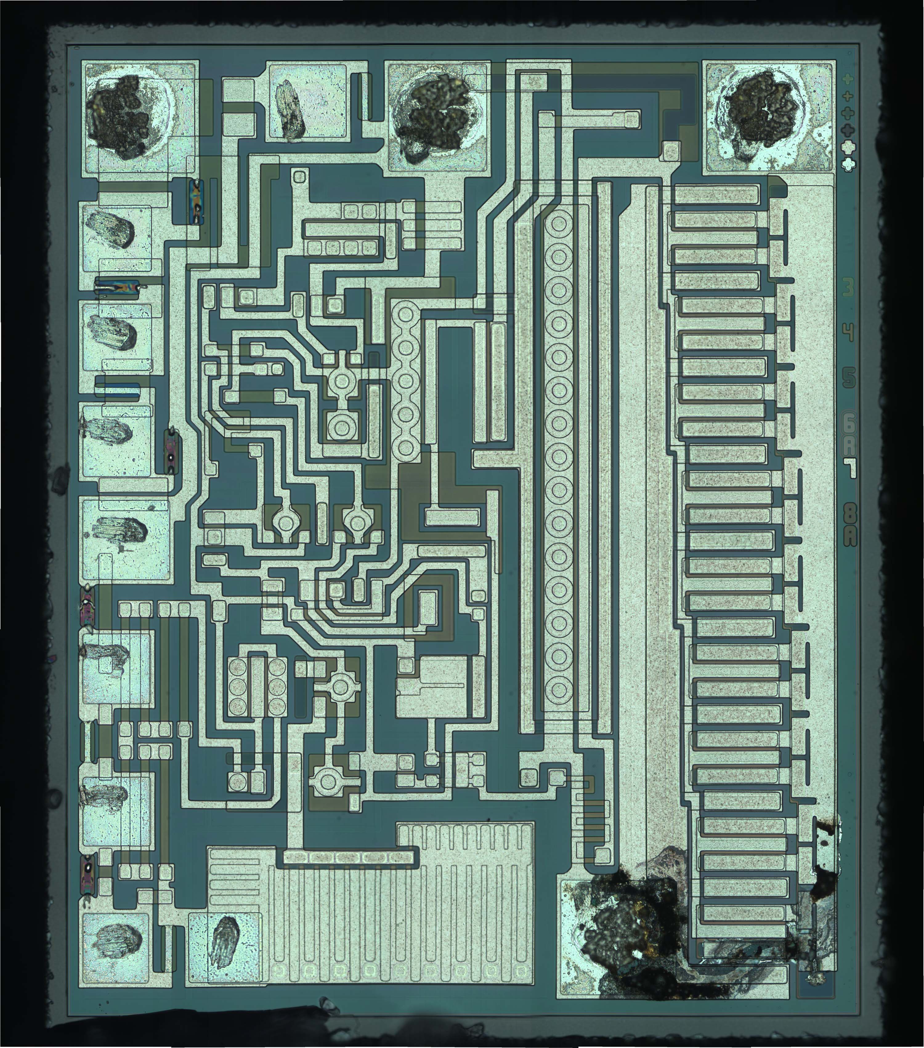
Here is an overview of the damaged chip (click on the image for a much larger version).

The spot with ESD damage is in the lower right hand corner, zoomed in here.

The path that the discharge event took between the output pin and the pass transistor of the regulator looks a little bit like a river channel that bends slightly up and over to the right. You can see how the metal was splattered and migrated by the ballistic motion of the electrons flowing by. This migration of metal eventually caused the pass transistor to get shorted out, so, unfortunately all the 3.3V devices downstream of this regulator got stuck with about 12V across them. Toasty! Fortunately, the PTC fuses on the board and other current-limiting mechanisms kicked in so the board never got dangerously hot.

One thing that struck me about this particular layout is the apparent lack of any on-chip ESD protection devices. Even though this is a big bad analog process, it seems non-intuitive to me that a bare device can stand up to the 2kV human body model tests that’s pretty much considered the minimum bar for ESD protection. Even if the device alone could stand up to the failure, it seems that what went wrong here was current arcing between two adjacent pieces of metal, possibly aggravated by the corona effect at the corners of the metal layout. At any rate, a device with no local ESD protection can be very susceptible, so perhaps even despite the precautions taken in the board layout, an external ESD event could blow up this chip.

I could be wrong, but perhaps I should now be looking for a chip vendor that was a little more fastidious about their ESD protection to prevent more unhappy customer return events. If any readers have some experience with analog chip processes like this, I’d appreciate a comment about the level of ESD protection you had to incorporate in your chip designs!

The ESD damage wasn’t the only interesting thing about the chip however. I also noticed burned out metal elsewhere on the chip:

There are several burned out spots like this on the left hand side of the chip.

This was a neat find, because this shows you how they trim these voltage regulators in the factory. For those not familiar with analog chip design, the accuracy of an integrated polysilicon resistor in an analog-optimized process is about +/- 20%. On a generic digital process, the accuracy is typically much worse (on the other hand, matching between devices on the same chip can be extremely tight and the quality of the match is proportional to the area of the device). Thus, when a chip advertises +/-1% accuracy for voltage, it has to have some kind of post-fabrication trimming mechanism built in.

Basically, the trim mechanism is constructed using a ladder of resistors in series, with shorting metal straps in parallel with each resistor. Therefore, when the chip is first manufactured, the calibration resistor ladder has a nominal resistance of nearly zero ohms. At wafer test, the chip’s output voltage is measured, and resistance is selectively added to this calibration ladder by using a series of high current is pulses to selectively blow the metal straps. Thus, the native chip design, without calibration, always shoots too far one way on the voltage, so you can always correct the problem by only adding resistance to a calibration ladder. If they did the design right, they would have it start with the voltage too low, so that if a fuse was only partially blown and it managed to repair itself (this does happen), you would only end up passing too little voltage to the regulated load, instead of too much — under the theory that if you are to have a malfunction, it’s typically safer to push less voltage than too much.

You can see all the extra bond pads used for this calibration process along the left hand side of the chip. There are very deep “scrub” marks, so large, heavily weighted needles were used to touch down on the wafer. This was probably necessary because of the high currents required to blow the metal fuses. Other trim mechanisms I’ve heard of include poly fuses, eFuses, or laser trimming, but I had never seen one “in real life” — they had always been an intellectual curiosity that I’ve read about in a process manual or a journal paper.

Wow, this post turned out long…

Name that Ware October 2007

Saturday, November 3rd, 2007

The ware for October 2007 is below. Click on the image for a much larger version.

This ware is a 100% mechanical piece that I think is particularly neat — it was given as a gift to me by one of Chumby’s vendors in China. I’ll tell you more about it when I name the winner next month!

Winner of Name that Ware September 2007!

Saturday, November 3rd, 2007

Last month’s challenge was not necessarily to name a particular device, but rather to name the type of device that generates a class of audible interference. You can listen to the sound again if you need your memory jogged!

While many immediately recognized the sound as interference caused by a GSM or EDGE phone, Jered wins the prize for his very precise analysis of the root cause of the noise:

The reason for the buzz is the nature of time-division mulitple access (TDMA). In the US, we operate mobile phones at 850 Mhz and 1900 Mhz; in Europe, 900 Mhz and 1800 Mhz. Good so far; that’s not going to make noise that we can hear. TDMA fits more subscribers into the same bandwidth by assigning different terminals different timeslots (vs. CDMA, which uses black magic). These timeslots happen to be spaced 4.615 ms apart, yielding a signal envelope which looks a lot like a dirty 217 Hz square wave.

All sorts of things (like “wires”) are good at picking up a 217 Hz square wave at 0.5 W, and 217 Hz is conveniently smack dab in the middle of our auditory capabilities.

Congratulations Jered! Email me for your prize.

I thought this noise was noteworthy because a surprising number of people do not realize where it is coming from. I’ve often heard this noise on conference calls, and its fairly obvious that some participants don’t understand that their cell phone is causing this interference. The thing that befuddles most is the range at which this interference can occur: their phone could be well across the table, yet with the proper antenna orientation, the noise is loud and clear. Often times, the problem can be ameliorated simply by rotating the phone by about ninety degrees.

What disturbs me about this noise is that it’s a prominent reminder of exactly how powerful this RF transmitter is that I happily stick next to my cerebral cortex and my gonads on a daily basis. 0.5 watts is not a trivial amount of power! And of course, Bluetooth hands-free sets are not much better. Granted the power is lower, but Bluetooth operates at 2.5 GHz — and it’s no mistake that microwave ovens also run at that frequency, as it is absorbed particularly well by the water that makes up 60% of our mass.

While there is no conclusive evidence that cell phones cause any sort of biological harm, there is precedent for entire societies that have fallen victim to the myopic use of technology to better life. For example, even a child can tell you today that lead causes poisoning and brain damage…and so we remark at the Roman’s folly: “Gosh, what idiots! They sweetened their wine with lead and used lead pipe to deliver drinking water. Duh, of course the Roman empire collapsed.”

I often wonder if a millennium from now, people will read about us as we do about the Romans. “Gosh, what idiots. They stuck half a watt of radiation on their heads every day for decades at a time. No wonder they all died of debilitating brain disease.” Or, my other favorite is, “Gosh, what idiots! The made their clothes, cars, and even utensils out of plastics. Everyone knows that plastics outgas damaging free radicals. No wonder they all died of cancer”…and in the end, the meek did inherit the Earth.

Then again…there is no conclusive evidence that anything we do really causes that much damage. We’ve learned from the Romans and gotten more clever, and we use “model” organisms and sophisticated extrapolation mechanisms. But then again, those are just models, and there’s no such thing as accelerated lifetime testing on a real human being…and as any engineer knows who has done a lot of reliability testing, there’s always that one corner case that gets through (e.g., the Xbox360 Red Ring of Death). So with enough new technology entering our lives, the chance that we’ll encounter unforeseen consequences goes up and up. You and me — we’re the ultimate guinea pigs in this grand experiment with technology!